EP0904655B1 - Procede et systeme d'etalonnage pour dispositifs de formation d'images - Google Patents
Procede et systeme d'etalonnage pour dispositifs de formation d'images Download PDFInfo
- Publication number
- EP0904655B1 EP0904655B1 EP97925068A EP97925068A EP0904655B1 EP 0904655 B1 EP0904655 B1 EP 0904655B1 EP 97925068 A EP97925068 A EP 97925068A EP 97925068 A EP97925068 A EP 97925068A EP 0904655 B1 EP0904655 B1 EP 0904655B1
- Authority
- EP
- European Patent Office
- Prior art keywords
- pixel
- pixel cell
- output
- values
- radiation
- Prior art date
- Legal status (The legal status is an assumption and is not a legal conclusion. Google has not performed a legal analysis and makes no representation as to the accuracy of the status listed.)
- Expired - Lifetime
Links
Images


Classifications
-
- H—ELECTRICITY
- H04—ELECTRIC COMMUNICATION TECHNIQUE
- H04N—PICTORIAL COMMUNICATION, e.g. TELEVISION
- H04N25/00—Circuitry of solid-state image sensors [SSIS]; Control thereof
- H04N25/50—Control of the SSIS exposure
- H04N25/57—Control of the dynamic range
- H04N25/571—Control of the dynamic range involving a non-linear response
-
- H—ELECTRICITY
- H04—ELECTRIC COMMUNICATION TECHNIQUE
- H04N—PICTORIAL COMMUNICATION, e.g. TELEVISION
- H04N25/00—Circuitry of solid-state image sensors [SSIS]; Control thereof
- H04N25/60—Noise processing, e.g. detecting, correcting, reducing or removing noise
- H04N25/67—Noise processing, e.g. detecting, correcting, reducing or removing noise applied to fixed-pattern noise, e.g. non-uniformity of response
- H04N25/671—Noise processing, e.g. detecting, correcting, reducing or removing noise applied to fixed-pattern noise, e.g. non-uniformity of response for non-uniformity detection or correction
-
- H—ELECTRICITY
- H04—ELECTRIC COMMUNICATION TECHNIQUE
- H04N—PICTORIAL COMMUNICATION, e.g. TELEVISION
- H04N25/00—Circuitry of solid-state image sensors [SSIS]; Control thereof
- H04N25/70—SSIS architectures; Circuits associated therewith
- H04N25/76—Addressed sensors, e.g. MOS or CMOS sensors
-
- H—ELECTRICITY
- H04—ELECTRIC COMMUNICATION TECHNIQUE
- H04N—PICTORIAL COMMUNICATION, e.g. TELEVISION
- H04N25/00—Circuitry of solid-state image sensors [SSIS]; Control thereof
- H04N25/30—Circuitry of solid-state image sensors [SSIS]; Control thereof for transforming X-rays into image signals
Definitions
- the invention relates to a system and method for calibrating and correcting the output of a semiconductor imaging device.
- Calibration techniques are typically used on a variety of devices to determine a scale that defines the true value of a parameter as a function of the device output. For example calibration is applied in calorimeters and spectrometers in order to identify the energy spectrum output from the device. Typically, calibration involves operating the device under known conditions, for example known amount of energy impinging on a calorimeter, and determining the output as a function of these conditions. During subsequent operation the calibration function is inverted and the output from the device is used to derive the impinging energy using the inverse calibration function.
- EP 0601 534 discloses a method of calibration of an infrared imaging device with compensation for non-uniformity of infrared focal plane arrays.
- the calibration operation measures the response generated by detector elements in the focal plane array to a wide range of known signal flux levels of infrared radiation produced by a umform black body under controlled conditions.
- This type of method has many disadvantages. For example, an expensive radiation source is required. Also, multiple radiation exposures are needed each time the imaging device is to be calibrated.
- JP07/236093 and JP07/236094 describe CCD systems which apply a correction factor to pixel outputs to derive a value representative of the optical light incident on the pixels of a CCD device.
- JP07/236093 the correction is applied for the ambient photodetector dark current.
- the charge per pixel due to the dark detector current is stored and then applied as a correction value to the pixel outputs to give a corrected value for the light incident on the pixels when light is present.
- JP07/236094 a reference image sensor is used to store a value for converting a charge value to an amount of incident light and then this 'correction' value is applied to the output of the real image sensor to convert charge into a value representative of the light incident on the imaging device.
- Imaging devices, systems and methods for performing high energy radiation imaging are disclosed in WO-A-95/33332 owned by the assignee of the current application.
- the imaging devices allow multiple successive radiation hits at a pixel detector location (pixel cell) to be converted in a semiconductor substrate into respective charge pulses.
- the charge pulses at each pixel detector location are accumulated on a respective pixel circuit.
- the accumulated charge which can correspond to tens, hundreds or thousands of radiation hits, is then output and digitized to produce an image pixel value that ideally should be equivalent to the number of accumulated radiation hits for the corresponding pixel location.
- Each imaging device comprises tens or even hundreds of thousands of pixels.
- Each pixel circuit carries its own charge accumulating capacitance and its own switching and protection components, all of which are identical only to the extent of the limits of current or future processing technology (e.g., ASIC technology). This means in practice that there is non-uniformity in the pixel arrays.
- the output from each pixel should ideally be linearly related to the number of accumulated radiation hits at that pixel, but in practice the relationship is non-linear.
- a method of calibrating pixel values output from respective pixel cells of an imaging device each of said pixel cells comprising a pixel circuit for accumulating charge in response to radiation incident on said imaging device comprising:
- Step (a)(i) preferably comprises, for each pixel cell, fitting pixel input values as a function of corresponding pixel output values to provide a parameterized relationship between the pixel input values and the corresponding pixel output values.
- the response function is preferably determined by varying externally a pixel input to the pixel cells and recording the pixel output value.
- the externally varied pixel input value can be a voltage value of a charge storing means of the pixel cell, for example a FET and/or a capacitor.
- step (a)(ii) comprises providing a pixel input signal to the pixel cells and recording the output of the respective pixel cells.
- the pixel input signal can be an amount of radiation from an external source.
- the output pixel value from a pixel cell for the amount of radiation defines the scale parameter for the pixel cell.
- step (a)(i) is performed before step (a)(ii) and the scale parameter is derived by inputting the output pixel value from the pixel for the amount of radiation to the response function.
- the table preferably has, at each entry, fitted parameters of the response function and the scale parameter for a respective pixel cell.
- pixel input values are preferably fitted as a function of the corresponding pixel output values to provide a parameterized relationship between the pixel input values and the corresponding pixel output values.
- the table has at each entry fitted parameters of the conversion function for a respective pixel cell.
- the table values are determined prior to image acquisition.
- the table is then used during image acquisition or otherwise before image display to convert pixel output values for respective pixel cells to provide converted output values for those pixel cells.
- the converted output values are linearly related to the number of accumulated radiation hits or to the accumulated amount of light on the corresponding pixel cell. However, other relationships could be generated if required.
- the method can also include updating the table with new values when factors which influence pixel cell performance change, for example where factors include temperature variations, signal integration times, exposure times, etc. change.
- an imaging system as defined in claim 18, comprising an imaging device having an array of pixel cells for producing pixel output values for generating a digital image.
- a map (table) with an entry, having a set of parameters, for each pixel is created, each entry containing all necessary parameters for that pixel to correct for the non-linear response of each pixel output to incident radiation and for the non-uniformity between pixels.
- the grey or colour scale assigned to each pixel value can be made directly and linearly proportional to the total number of radiation hits accumulated in the pixel.
- another desired relationship between the grey or colour scale assigned to each pixel and the number of radiation hits accumulated in the pixel could be generated instead.
- the present invention finds particular application to multiple hit charge accumulation devices such as is described in WO-A-95/33332.
- Such devices provide the advantage of being able to accumulative radiation incident on a pixel cell, with the result that it can cope with any practically useful radiation intensity when single hit counting is simply not feasible.
- Applications with high radiation intensity include, but are not limited to, conventional X-ray radiography, mammography, X-ray real time imaging etc.
- the calibration map can be created once before every image or more rarely if the pixel device and its environment do not change substantially (e.g. once a day or once a month).
- the calibration map is preferably stored after conversion in an analog to digital converter (ADC), for example on an ADC card or in a computer used for image processing and display.
- ADC analog to digital converter
- Figure 1 is a schematic representation of an example of an imaging system 10 including an imaging device as described in WO-A-95/33332. As illustrated the imaging system is used for imaging of an object 12 subjected to radiation 14.
- the radiation may, for example, be X-ray radiation and the object 12 may, for example, be a part of a human body.
- the imaging device comprises an Active-pixel Semiconductor Imaging Device (ASID) 16 comprising a plurality of pixel cells 18.
- the imaging device detects directly high energy incident radiation such as X-rays, ⁇ -rays, ⁇ -rays or ⁇ -rays and accumulates at each pixel cell, by means of a randomly accessible, active, dynamic pixel circuit on or adjacent to a corresponding pixel cell detector, values representative of the radiation incident at that pixel cell.
- the ASID can be configured as a single semiconductor substrate (e.g., silicon) with each pixel cell comprising a pixel detector 19 and an active pixel circuit 20.
- the ASID can be configured on two substrates, one with an array of pixel detectors 19 and one with an array of active pixel circuits 20, the substrates being mechanically connected to each other by, for example, conventional bump-bonding technology.
- Each pixel cell 18 is in effect defined on the substrate by electrodes (not shown) which apply a biasing voltage to define a detection zone (i.e., the pixel detector 19) for the pixel cell 18.
- Active pixel circuits 20 in the form of electronic structures (e.g., of transistors, capacitors, etc.) can be defined on each pixel cell 18 or at a corresponding location on the associated second substrate to accumulate charge created in the pixel detector when, for example, a photon or a charged particle of radiation is incident on the semiconductor detection zone of the pixel cell 18.
- An active pixel circuit 20 and the pixel detector 19 can be of the order of a few tens of microns in size (e.g., 10-50 ⁇ m). An example of an active pixel circuits is described with reference to Figure 2.
- the pixel detectors 19 are formed with a detection zone such that, when a photon is photo-absorbed in the semiconductor substrate 16 at a pixel cell 18 creating an electric charge or when a charged radiation ionizes the detection zone of the semiconductor substrate 16 at a pixel cell 18, an electric pulse flows from the semiconductor substrate detection zone to the active pixel circuit 20 for that pixel cell 18. A value associated with the electric pulse is then accumulated in an active circuit element, either directly as a charge value or as an equivalent voltage or current value such that new charge created from subsequent incoming radiation is added continuously. Examples of possible accumulating devices are an integrated capacitor or the gate of an integrated transistor.
- the charge accumulation process in an active pixel circuit 20 continues until control signals are issued from control electronics 24 to start a process of reading out information by addressing each pixel cell, effectively in a random access manner, from each individual pixel cell.
- control signals are issued from control electronics 24 to start a process of reading out information by addressing each pixel cell, effectively in a random access manner, from each individual pixel cell.
- charge continues to be accumulated because the readout is always done individually for detecting pixel cells.
- Pixel circuits may selectively be reset after readout to discharge the charge accumulation circuit elements, and only then are pixels inactive for a very short time (practically no dead time as will be shown). Thus, only during resetting are individual pixels inactive.
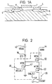
- Figure 1a shows the charge accumulation principle of one example of a pixel circuit charge accumulation element.
- a field effect transistor is formed on a semiconductor substrate. Specifically, n+ doped regions 4 and 6 are formed for the source and drain, respectively, in a P-type silicon substrate 1. Electrodes for the source 3 and drain 5 are formed in an oxide layer 2, a gate electrode 7 being formed over the oxide layer 2. Charge is accumulated on the gate electrode 7 of a field effect transistor (MOSFET) by virtue of the FET gate capacitance. As charge accumulates on the FET gate it decreases the electron concentration in the FET inversion layer 8 (the layer with minority-electron carriers needed for the FET operation). The maximum charge that can be accumulated depends on the minimum allowable electron density in the inversion layer.
- MOSFET field effect transistor
- Charge accumulation is therefore not affected by any dark current coming from the bulk silicon as in the case of a CCD, because charge is not accumulated in any depleted volume.
- Charge accumulation capacity is determined only by the total FET gate area (which can be substantially close to the pixel circuit area), the oxide layer thickness (which can be as thin as few nm or tens of nm) and the FET dynamic range (which determines the maximum gate voltage). It should be noted that this is just an example of a pixel circuit charge accumulation element, and charge can be accumulated in any suitable charge accumulating means implemented in the corresponding pixel circuit.
- the pixel pitch can be as small as 10 ⁇ m which results in excellent position resolution and consequently excellent image resolution.
- FIG. 2 illustrates one preferred example of an active pixel circuit 20 for a pixel cell in an example of an imaging device using field effect transistors (FETs) arranged as a cascode connected amplifier.
- VBIAS 40 is a bias voltage input across the detection zone forming the pixel detector 19 of the pixel cell.
- the pixel detector 19 is represented by the diode symbol D11.
- SIGOUT 42 is an analogue signal output and VANA 44 an analogue power supply input.
- RES-R-1 is a reset input and ENA-R-1 is an enable input for the pixel circuit. Charge is accumulated in the gate of a transistor M11A 50 when both the RES-R-1 46 and ENA-R-1 48 inputs are low.
- the gate capacitance substantially forms the input node capacitance (total capacitance) thus maximizing charge storage ability.
- substantially all of the input node capacitance arises from the charge accumulation transistor M11A 50.
- the M11A 50 capacitance can be 2pF and the FET gate voltage dynamic range can be at least 2Volts. This corresponds to about 25,000,000 electrons in storage capacity which is more than 100 times the capacity of a CCD of the same pixel size. It should be noted that the 2pF of the FET capacitance in the above example substantially forms all of the input node capacitance of the pixel cell.
- the total parasitic capacitance of the detector and the other elements in each pixel circuit and corresponding pixel detector is in the range of a few fF or tens of fF.
- the capacitance of the charge storage device should be maximized and in any case be substantially bigger than the parasitic capacitance in each pixel cell.
- the capacitance of the FET acting as a charge accumulating device in the pixel circuit is more than 90% of the total capacitance of the pixel cell comprising a pixel detector and the corresponding pixel circuit. As a result of this, substantially all collected charge will be accumulated in the charge accumulating FET rather than being shared among the detectors, and the rest of the pixel circuit elements.
- this circuit provides an example, only, where charge accumulating capacitance is maximised using a pixel charge storage device (such as a FET gate or a capacitor) that accounts for most of the input node capacitance for each pixel.
- a pixel charge storage device such as a FET gate or a capacitor
- ENA-R-1 is taken to a high state, which allows current to flow from the transistor M11A 50 through the transistor M11B 52 to SIGOUT 42.
- the pixel circuit is reset by taking RES-R-1 to high, whereupon after RES-R-1 has been at high for merely a few microseconds, any accumulated charge will have been removed from the gate of the transistor M11A 50. Immediately after RES-R-1 46 goes to a low level, charge can begin to accumulate at the gate of the transistor M11A 50.
- Figure 3 is a schematic representation of one possible configuration of the control electronics 24 of Figure 1 and the relationship of the control electronics 24 to an m x n matrix of the active circuits 20 of the pixel cells 18.
- an array of 9 pixel cells is illustrated in Figure 3 and only some of the signal lines which make up the path 22 in Figure 1 are shown. It will be appreciated that an imaging device will normally include a significantly larger number of pixel cells than are shown in Figure 3.
- the row select logic 60 controls the row readout (ENA 74) and the row reset (RES 76) and the column logic 62 enables (COL-SEL) the readout of accumulated charge values from each pixel circuit 20 in response to a clock signal 79.
- the control electronics 24 include row select logic circuits 60, column address logic circuits 62, power supply circuits 70, Analogue to Digital Converter (ADC) 56 and the signal processing circuits 58. Preferably some, if not all, of the control electronics 24 is implemented on the substrate 16 at the periphery of the image array formed by the array of pixel cells 18.
- ADC Analogue to Digital Converter
- the power supply circuits 70 provide power for the individual active circuits 20 on the pixel cells 18 via lines 54 (shown schematically in Figure 3) and can additionally be arranged to supply the biasing voltage via lines (not shown) for the electrodes defining the pixel cells.
- the row select logic 60 provides signals via row enable and reset lines 64 and 66, respectively (also shown schematically in Figure 3), for selecting columns for the reading and resetting, respectively of the individual active circuits 20 of the pixel cells 18.
- the row select 64 and row reset 66 lines are connected to the enable input ENA-R-1 48 and the reset input RES-R-1 46, respectively of each of the pixel circuits of the row.
- row enable 74 and row reset 76 signals for scanning successive rows. It can be seen that the reset pulse 76 follows the row enable pulse 74 to cause resetting of the active circuits after reading.
- the column select logic 62 effectively comprises a multiplexer for selecting signals output via the column lines 68 (also shown schematically in Figure 3), each column line being connected to the SIGOUT output 42 of each pixel circuit 20 in that column.
- the COL-SEL signal 78 represented in the column select logic 62 thus selects columns for reading the individual active circuits 20 of the pixel cells 18 currently selected by the row enable pulses 74.
- the column select pulse is clocked for successive column positions in response to the clock CLK 79 during one row enable period, so that the accumulated charge value of a respective active pixel circuit on the row currently selected is clocked out at each clock pulse before the row select pulse proceeds to the next row.
- Each active pixel circuit of the row just read is then reset simultaneously by the row reset pulse 76.
- each pixel charge value is digitized in an ADC and then output to the image processor as a digital pixel output value in the form of an ADC count for each pixel cell.
- the device output is an array ADCi, where the subscript refers to the pixel number.
- the number of ADC counts for a pixel i is a measure of the analog charge value that was stored on that pixel.
- any pixel should provide the same output (a current or a voltage value).
- the output of the pixel should ideally respond linearly by providing double or triple output current (or voltage). In practice, however, non-uniformity between individual pixels and non-linear response of each pixel occur.
- the mapping function for the output value correction in an embodiment of the invention is extracted using data from the imaging device itself and not from a reference sensor/device.
- a reference sensor/device will always be only approximately similar to the imaging device and cannot exactly reflect the non-linear response and non-uniformity of the imaging device.
- the present invention is not limited to this preferred embodiment and can be applied to other semiconductor pixel imaging devices and systems, for example CCD-based systems or systems having pixel devices employing thin film technology (Amorphous Si, Selenium devices etc.).
- Each pixel in a semiconductor imaging device has charge storage means for storing charge created from converted incoming radiation.
- the devices described WO-A-95/33332 comprise a charge storage device in the form of a capacitor and/or a Field Effect Transistor (FET), in other imaging devices charge can also be stored in the stray pixel capacitance.
- Stored charge changes a feature of the charge storing device. For example, if the charge storing device is a FET then stored charge changes the voltage of the gate where the charge is stored. A different gate voltage will result in a change in an output from the pixel, usually either a change in a voltage or a current output value.
- a parameter that determines the amount of stored charge is varied externally.
- the output of the pixel is digitized to provide an ADC count value.
- a function is then fitted between the input and digitized output values to determine a relationship between the ADC count values and the corresponding pixel parameter values, which in turn relates to the stored charge.
- the FET for each pixel cell accumulates charge from pulses generated in a corresponding pixel detector for the pixel cell in respect of respective radiation hits.
- the FET gate where the charge is accumulated is reset at the beginning of each cycle of operation to a certain voltage, for example 5 Volts. Then as electrons are accumulated in response to the pulses from respective radiation hits, the gate voltage drops.
- V the difference in the gate voltage (a value between 0 and 5 Volts)
- Q the accumulated number of electrons
- C the FET gate capacitance
- the final gate voltage results in a pixel output value being formed, which in most cases is either a voltage or a current value.
- This pixel output value is then digitized.
- the FET gate reset voltage is adjusted externally, for example to 3Volts, by applying 3Volts over lines 54 to the power supply inputs VANA 44 of each of the pixel circuits (i.e. to VR4 in Figure 4). This is equivalent to the reset being 5Volts and then dropping by 2 Volts because of accumulated electrons.
- the use of the externally applied selective reset voltage can simulate the effect of number of radiation hits, in a manner which can be replicated in each of the pixel cells.
- the response of the pixel cell is equivalent to result of accumulated electrons dropping the gate voltage by 2 Volts.
- the pixel output for different reset voltages is recorded in terms of the respective ADC counts. For each reset voltage value a certain number of ADC counts will be obtained.
- the relationship between the reset voltage values and the ADC counts is then fitted to a function (for example a quadratic function) to obtain a function for computing the relationship between voltages at the gate where electrons are being accumulated and the ADC counts.
- an embodiment of the invention can also address the problem of how to account for non-uniformity between pixels.
- the final ADC counts that will be assigned grey or colour values should reflect the total charge on each pixel and not just the voltage of the FET gate. Therefore, a correction is applied for this non-uniformity between pixels.
- an 'empty' image is accumulated using a radiation source (for example and X-ray source) without an object between the radiation source and the imaging device. In this way some amount of radiation enters each detector pixel.
- the pixel outputs are then recorded and used to obtain a scale parameter.
- a scale parameter is obtained through the response function defined previously for a given pixel output value. This is called a scale parameter for a given pixel because any subsequently obtained pixel input value with the radiation source and object to be imaged will be compared to it and the corrected pixel value will be defined with respect to this parameter.
- the scale parameter is derived by inputting the output pixel value from the pixel for the amount of radiation to the response function.
- the method comprises a step of obtaining the non-linear response of each pixel to incident radiation and a second step of obtaining the non-uniformity correction between pixels.
- a table, or map, or array with one entry per pixel is stored, possibly on a card carrying the ADCs 56, or possibly in a memory of a computer forming the image processor 28 for generating images from the pixel data.
- Each entry in the table comprises a number of parameters defining a response function for each pixel and a scale parameter to account for non-uniformity between pixels.
- FIG 4 is a schematic presentation of a single pixel circuit and its associated readout process.
- a reset FET 81 can initialize the gate voltage of a charge storing FET 82 to some user defined value. After the charge storing FET 82 has been reset to some value V R , it accumulates charge for a predetermined period of time t i .
- the gate voltages create a current in FET 82 when that pixel is been read out by changing the control voltages Col xxx and Row xxx in FET 85 and FET 86. This current generates a voltage over resistor R1 in amplifier A1 87.
- the signal is further amplified in amplifier A2 88 defined by resistor values R2 and RA and offset by voltage V2 for the ADC 90 input level 89.
- the FET 82 During the integration period for accumulating charge, if there is no signal from X-rays (or other radiation) the FET 82 accumulates the charge from the detector leakage current I dl .
- FIG. 6 shows the relationship of the reset voltage to the number of ADC counts.
- a second order polynomial (for example as represented schematically in Figure 8) is fitted to the respective curves to define the response function for each pixel circuit.
- the response function is non-linear. This means that double or triple voltage drops on the FET 82 charge storing gate does not produce two or three times the output at the ADC level.
- the second step of the calibration is to take into account that the pixels do not have identical characteristics, such as charge storing capacitance.
- the variation on the capacitances of each pixel can be of the order of 10%.
- the pixel non-uniformity is eliminated as follows.
- the grey or colour scale value assigned to each pixel value should be related to the ratio of received radiation hits (e.g. X-rays) to the maximum number of radiation hits (X-rays) received if no-object is imaged. This way the total number of available display scales is evenly divided according to the number of X-rays. Each pixel receives some current of X-rays Is during the exposure time ts.
- Figure 5 illustrates what happens when a flux of X-rays (the signal) is absorbed during time ts.
- the starting reset voltage is VR.
- Curve 121 shows that charge accumulated because of the X-rays adds up to the charge from the detector leakage current.
- Curve 122 shows that after the X-ray exposure is completed the detector leakage current continues to be accumulated.
- V G x - rays ( t i ) V R - I DL • t i C F - I S • t S C F (where I S is the charge current created from the incoming flux of X-rays, t s is the X-ray exposure time and V R is the reset voltage chosen for the operation of the imaging device).
- ADC Xmax can be identified, which represents the maximum expected signal from X-rays.
- V RXmax V R - I S •t S C F
- N I S I Smax N
- V Rxmax is the scale parameter, which, as can be seen from the above equation, defines the total scale or range for the pixel cell as identified in Figure 6. From the above equation it can be seen that the effect of the capacitance of each individual pixel is cancelled out. Basically this is achieved by taking an empty exposure and recording the maximum response of each pixel ( i.e. V Rxmax ).
- the values of the polynomial coefficients (a i , b i and c i - see Figure 8) and the scale parameter (SP i ) are stored for each pixel (at a respective addressable entry in a table T - see Figure 7) as parameters defining a conversion function representative of a non-linear response of a pixel cell and/or differences between pixel cells. This is then used during image acquisition or before image display to correct for the non-linear response of a pixel cell and/or differences between pixel cells.
- each digital pixel value is adjusted to correct for possible non-linear response of the output of each pixel to its input. Furthermore the digital pixel values are adjusted to account for their non-uniform characteristics, such as non-identical charge storing capacitances.
- the calibration/correction for the non-linear response of each pixel individually is achieved by varying externally the input parameter that influences the pixel output and recording the digital pixel output as a function of the known input parameter. The function is then reversed to acquire the pixel analog input values as a function of the digital output values.
- the calibration/correction for the non-uniform pixel characteristics is done by recording the maximum and minimum output of each pixel individually to some flux of incoming radiation and no flux respectively. When imaging an object, each image pixel will then experience a condition between these two extremes.
- the aim of the current invention to provide a method for relating the output of each pixel to the amount of incident radiation taking correctly into account the non-linear response of each pixel individually to the incident radiation and the non-uniformity among pixels. It is evident that the method described above takes correctly into account other more trivial effects such as for example the continuous detector leakage (or dark) current.
- the calibration method disclosed offers fine images not only in connection of perfected pixel values but also in connection of combined pixel values to acquire an image of a low contrast object. In such a case pixel values must be corrected prior to combination and display to provide accurately the information about the total initial number of incident radiation hits for each group of pixels.
- the calibration/correction map (table) containing the response function and non-uniformity correction for each pixel is preferably stored at the ADC card or at the image processor (computer) stage.
- Each pixel has a correction entry in the calibration map that requires 4 bytes of disk space or even less if data compression techniques are employed.
- the addressing of the table can be directly in response to the addressing of the array of pixels (e.g. using the address signals from 60 and 62 in Figure 3), or alternatively the addressing can be done after initial storage of the pixel output values. Therefore the calibration map poses no difficulty to existing commercially available ADC and computer systems.
- the above calibration technique is particularly intended for displaying images acquired with the imaging device disclosed in WO-A-95/33332, it will be appreciated that it can be applied to improve and perfect images acquired with some other pixel semiconductor imaging devices such as CCDs, amorphous Si pixel devices, thin film employing pixel devices etc. It will also be appreciated that the above disclosed method can also perfect images acquired in the infrared, optical and other part of the spectra besides high energy radiation (such as X-rays, gamma rays, beta rays, alpha rays etc.)
- high energy radiation such as X-rays, gamma rays, beta rays, alpha rays etc.
- a conversion function is determined by externally applying reset voltages to determine a response function for each pixel cell as representative of the non-linear relationship of the pixel output values to pre-defined pixel input values and then irradiating the imaging device to determining a scale parameter for each pixel cell as representative of non-uniformity between pixel cells from the relative pixel output values for a given input radiation intensity.
Landscapes
- Engineering & Computer Science (AREA)
- Multimedia (AREA)
- Signal Processing (AREA)
- Physics & Mathematics (AREA)
- Nonlinear Science (AREA)
- Transforming Light Signals Into Electric Signals (AREA)
- Solid State Image Pick-Up Elements (AREA)
- Closed-Circuit Television Systems (AREA)
- Measurement Of Radiation (AREA)
- Testing, Inspecting, Measuring Of Stereoscopic Televisions And Televisions (AREA)
- Measurement Of Velocity Or Position Using Acoustic Or Ultrasonic Waves (AREA)
- Image Input (AREA)
- Facsimile Image Signal Circuits (AREA)
- Analysing Materials By The Use Of Radiation (AREA)
- Dot-Matrix Printers And Others (AREA)
- Ultra Sonic Daignosis Equipment (AREA)
- Recording Measured Values (AREA)
Claims (21)
- Procédé d' étalonnage de valeurs de pixels fournies en sortie par des cellules de pixels respectives d'un dispositif de formation d'image, chacune desdites cellules de pixels comprenant un circuit de pixel (20) pour accumuler une charge en réponse à un rayonnement incident sur ledit dispositif de formation d'image, le procédé comprenant :a) la détermination d'une fonction de conversion pour chaque cellule de pixel, ladite fonction de conversion étant représentative d'une réponse non linéaire d'un pixel et étant formée par la combinaison d'une fonction de réponse et d'un paramètre d' échelle, comportant les étapes suivantes :i) l'application de tensions d'entrée de circuits de pixels prédéfinies à chaque circuit de pixel, et la détermination de ladite fonction de réponse pour chaque circuit de pixel comme étant représentative de la relation entre des valeurs. de sortie de pixels et lesdites tension d'entrée de circuits de pixels prédéfinies appliquées ; etii) la détermination dudit paramètre d'échelle pour chaque cellule de pixel comme étant représentative des différences de charge accumulée stockée par différentes cellules de pixels en réponse à une intensité de rayonnement d'entrée appliquée ; etb) 1a définition d'une structure de données comprenant une entrée pour ladite fonction de conversion déterminée pour chaque cellule de pixel et accessible pour l'application de ladite fonction de conversion déterminée pour ladite cellule de pixel à une valeur déterminée à partir de la sortie de ladite cellule de pixel pour calculer une valeur corrigée ayant une relation souhaitée avec le rayonnement incident sur ladite cellule de pixel.
- Procédé selon la revendication 1, dans lequel l'étape (a)(i) comprend, pour chaque cellule de pixel, l'ajustement des valeurs d'entrée de pixels en fonction de valeurs de sortie de pixels correspondantes pour produire une relation paramétrée entre lesdites valeurs d'entrée de pixels et lesdites valeurs de sortie de pixels correspondantes.
- Procédé selon la revendication 1 ou la revendication 2, dans lequel ladite fonction de réponse est déterminée en faisant varier extérieurement un pixel fourni en entrée auxdites cellules de pixels et en enregistrant une valeur de sortie de pixel résultante.
- Procédé selon la revendication 3, dans lequel ladite valeur d'entrée de pixel amenée à varier extérieurement est une valeur de tension de réinitialisation d'un moyen de stockage de charge de ladite cellule de pixel.
- Procédé selon la revendication 4, dans lequel ledit moyen de stockage de charge comprend un transistor à effet de champ (FET) et/ou un condensateur.
- Procédé selon l'une quelconque des revendications précédentes, dans lequel l'étape (a) (ii) comprend la fourniture d'un signal d'entrée de pixel auxdites cellules de pixels et l'enregistrement de ladite sortie desdites cellules de pixels respectives.
- Procédé selon la revendication 6, dans lequel ledit signal d'entrée de pixel est une quantité de rayonnement appliquée par une source externe.
- Procédé selon la revendication 7, dans lequel ladite valeur de pixel de sortie provenant d'une cellule de pixel pour ladite quantité de rayonnement est utilisée pour définir ledit paramètre d'échelle pour ladite cellule de pixel.
- Procédé selon l'une quelconque des revendications précédentes, dans lequel l'étape (a) (i) est exécutée avant l'étape (a) (ii) et dans lequel ledit paramètre d'échelle est déterminé en fournissant en entrée à ladite fonction de réponse ladite valeur de pixel de sortie provenant dudit pixel pour ladite quantité de rayonnement.
- Procédé selon l'une quelconque des revendications précédentes, dans lequel ladite structure de données a pour chaque entrée des paramètres ajustés de ladite fonction de réponse et dudit paramètre d'échelle pour une cellule de pixel respective.
- Procédé selon la revendication 1, dans lequel l'étape a (ii) comprend l'enregistrement de la sortie maximum et minimum de chaque cellule de pixel, respectivement en réponse à un certain flux de rayonnement incident et à une absence de flux.
- Procédé selon l'une quelconque des revendications précédentes, dans lequel lesdites entrées de la structure de données sont déterminées avant l'acquisition d'image.
- Procédé selon l'une quelconque des revendications précédentes, comprenant l'utilisation de ladite structure de données pour convertir des valeurs de sortie de pixels pour des cellules de pixels respectives afin de fournir des valeurs de sortie converties pour ces cellules de pixels.
- Procédé selon l'une quelconque des revendications précédentes, dans lequel ladite relation souhaitée est une relation selon laquelle des valeurs de sortie converties sont liées linéairement au nombre de détections de rayonnement accumulées ou à la quantité accumulée de lumière sur ladite cellule de pixel correspondante.
- Procédé selon l'une quelconque des revendications précédentes, comprenant la mise à jour de ladite structure de données avec de nouvelles valeurs lorsque des facteurs qui influencent les performances des cellules de pixels varient.
- Procédé selon la revendication 15, dans lequel lesdits facteurs comprennent des variations de température, des temps d'intégration de signal, et des temps d'exposition.
- Procédé selon l'une quelconque des revendications précédentes, dans lequel lesdites valeurs déterminées à partir de la sortie de chaque cellule de pixel sont des valeurs numériques.
- système de formation d'image (10) comprenant un dispositif de formation d'image (16) ayant un groupement de cellules de pixels (18), chacune desdites cellules comprenant un circuit de pixel pour accumuler une charge en réponse à un rayonnement incident, et pour produire des valeurs de sortie de pixels pour générer une image numérique, ledit système comprenant :des moyens pour déterminer une fonction de conversion pour chaque cellule de pixel (18) en appliquant une tension d'entrée de circuit de pixel prédéfinie à chaque circuit de pixel, ladite fonction de conversion étant représentative d'une réponse non linéaire d'une cellule de pixel et/ou de différences entre des cellules de pixels et étant formée par la combinaison d'une fonction de réponse et d'un paramètre d'échelle, ladite fonction de réponse pour ladite cellule de pixel étant représentative d'une relation non linéaire de valeurs de sortie de pixels à des valeurs de tensions d' entrée de circuits de pixels prédéfinies et à un paramètre d'échelle pour chacune desdites cellules de pixels, qui est représentative de différences de charge accumulée stockée par des cellules de pixels différentes en réponse à une intensité de rayonnement d'entrée appliquée ;une structure de données (T) comprenant une entrée pour chaque cellule de pixel pour ladite fonction de conversion déterminée pour ladite cellule de pixel ; etdes moyens (28) pour calculer des valeurs de pixels corrigées pour une image numérique à partir d'une valeur déterminée sur la base de la sortie de chaque cellule de pixel en utilisant ladite fonction de conversion stockée pour ladite cellule de pixel dans l'entrée de la structure de données correspondante, lesdites valeurs de pixels corrigées fournies en sortie ayant une relation souhaitée avec un rayonnement incident sur ladite cellule de pixel.
- Système selon la revendication 18, comprenant des moyens de conversion analogiques et numériques (56, 90) pour numériser la sortie de chaque cellule de pixel, afin de former ladite valeur déduite à partir de celle-ci.
- Système selon la revendication 18 ou la revendication 19 , comprenant des moyens (28) pour calculer une valeur de sortie de pixel maximum pour une cellule de pixel correspondant à une quantité maximum prédéterminée de rayonnement incident sur ladite cellule de pixel, pour définir un maximum d' une échelle numérique pour ladite cellule de pixel.
- Système selon l'une quelconque des revendications 18 à 20, comprenant des moyens de stockage de charge, par exemple un FET (82) et/ou un condensateur.
Applications Claiming Priority (3)
| Application Number | Priority Date | Filing Date | Title |
|---|---|---|---|
| GB9612534A GB2314227B (en) | 1996-06-14 | 1996-06-14 | Calibration method and system for imaging devices |
| GB9612534 | 1996-06-14 | ||
| PCT/EP1997/002993 WO1997048225A1 (fr) | 1996-06-14 | 1997-06-09 | Procede et systeme d'etalonnage pour dispositifs de formation d'images |
Publications (2)
| Publication Number | Publication Date |
|---|---|
| EP0904655A1 EP0904655A1 (fr) | 1999-03-31 |
| EP0904655B1 true EP0904655B1 (fr) | 2004-02-18 |
Family
ID=10795342
Family Applications (1)
| Application Number | Title | Priority Date | Filing Date |
|---|---|---|---|
| EP97925068A Expired - Lifetime EP0904655B1 (fr) | 1996-06-14 | 1997-06-09 | Procede et systeme d'etalonnage pour dispositifs de formation d'images |
Country Status (8)
| Country | Link |
|---|---|
| EP (1) | EP0904655B1 (fr) |
| JP (1) | JP4169787B2 (fr) |
| AT (1) | ATE260014T1 (fr) |
| AU (1) | AU3033397A (fr) |
| DE (1) | DE69727673T2 (fr) |
| GB (1) | GB2314227B (fr) |
| NO (1) | NO985823L (fr) |
| WO (1) | WO1997048225A1 (fr) |
Cited By (1)
| Publication number | Priority date | Publication date | Assignee | Title |
|---|---|---|---|---|
| DE102005047595A1 (de) * | 2005-10-05 | 2007-04-12 | Carl Zeiss Sms Gmbh | Verfahren zur Ermittlung der Empfindlichkeit von Sensorarrays |
Families Citing this family (18)
| Publication number | Priority date | Publication date | Assignee | Title |
|---|---|---|---|---|
| FR2800549B1 (fr) * | 1999-11-02 | 2002-04-05 | Dominique Bertrand | Procede et dispositif d'acquisition de pixels |
| DE10057246A1 (de) * | 1999-12-11 | 2001-07-12 | Qualico Gmbh | Infrarot-Nachweisvorrichtung für eine Vorrichtung zum Erfassen von Eigenschaften einer bewegten Papierbahn mit Polychromator und IR-Detektormatrix |
| JP3754989B2 (ja) * | 2000-11-10 | 2006-03-15 | アークレイ株式会社 | センサ出力の補正方法 |
| EP1301031A1 (fr) | 2001-09-29 | 2003-04-09 | Philips Corporate Intellectual Property GmbH | Méthode de correction des charactéristiques de transfert différentes de capteurs d' images |
| GB0205482D0 (en) | 2002-03-08 | 2002-04-24 | Bae Systems Plc | Improvements in or relating to infra red camera calibration |
| JP2004077709A (ja) | 2002-08-15 | 2004-03-11 | Konica Minolta Holdings Inc | 画像入力装置及び画像入力方法 |
| DE10239994B4 (de) * | 2002-08-27 | 2006-12-14 | Robert Bosch Gmbh | Verfahren zur Korrektur von Ungleichmäßigkeiten eines Bildsensorsystems |
| US7443431B2 (en) * | 2002-09-13 | 2008-10-28 | Eastman Kodak Company | Fixed pattern noise removal in CMOS imagers across various operational conditions |
| EP1429542A1 (fr) * | 2002-12-11 | 2004-06-16 | Dialog Semiconductor GmbH | Compensation de bruit d'un motif fixe avec exigence réduite de mémoires |
| EP1795918B1 (fr) | 2004-07-06 | 2013-02-27 | Oy Ajat Ltd. | Système d'imagerie de rayons X de conversion à rayonnement direct, à forte énergie, en temps réel, pour des appareils photographiques à base de CD-TE et CD-ZN-TE |
| US20060011853A1 (en) | 2004-07-06 | 2006-01-19 | Konstantinos Spartiotis | High energy, real time capable, direct radiation conversion X-ray imaging system for Cd-Te and Cd-Zn-Te based cameras |
| US8049293B2 (en) | 2005-03-07 | 2011-11-01 | Sony Corporation | Solid-state image pickup device, electronic apparatus using such solid-state image pickup device and method of manufacturing solid-state image pickup device |
| TW201101476A (en) | 2005-06-02 | 2011-01-01 | Sony Corp | Semiconductor image sensor module and method of manufacturing the same |
| DE102005043048A1 (de) * | 2005-09-09 | 2007-03-22 | Siemens Ag | Verfahren zur Korrektur eines Bilddatensatzes sowie Verfahren zur Erstellung eines Bildes |
| EP1959674A1 (fr) * | 2007-02-08 | 2008-08-20 | Texmag GmbH Vertriebsgesellschaft | Caméra et son procédé de fonctionnement |
| JP4895391B2 (ja) * | 2007-09-03 | 2012-03-14 | キヤノン株式会社 | 画像読み取り装置 |
| JP6790054B2 (ja) * | 2018-04-20 | 2020-11-25 | シャープ株式会社 | 撮像システム、撮像システムの制御方法、および制御プログラム |
| US10866332B2 (en) | 2018-04-20 | 2020-12-15 | Sharp Kabushiki Kaisha | Imaging system, control method of imaging system, and storage medium |
Family Cites Families (24)
| Publication number | Priority date | Publication date | Assignee | Title |
|---|---|---|---|---|
| EP0024470A3 (fr) * | 1979-08-21 | 1981-05-06 | Ball Corporation | Procédé et appareil pour compenser les variations de sensibilité dans un capteur d'image |
| GB2149605B (en) * | 1983-11-04 | 1987-06-10 | Marconi Avionics | Image processing |
| DE3732820A1 (de) * | 1987-09-29 | 1989-04-06 | Siemens Ag | Bilddetektor |
| JPH01235484A (ja) * | 1988-03-16 | 1989-09-20 | Toshiba Corp | 画像読取装置 |
| JPH0671309B2 (ja) * | 1988-04-21 | 1994-09-07 | 沖電気工業株式会社 | イメージセンサの出力補正方法 |
| US4920428A (en) * | 1988-07-08 | 1990-04-24 | Xerox Corporation | Offset, gain and bad pixel correction in electronic scanning arrays |
| JP2743427B2 (ja) * | 1989-01-13 | 1998-04-22 | 日本電気株式会社 | 赤外線撮像装置 |
| JPH03246428A (ja) * | 1990-02-23 | 1991-11-01 | Fujitsu Ltd | 赤外線映像装置 |
| US5086343A (en) * | 1990-05-11 | 1992-02-04 | Eastman Kodak Company | Method and apparatus for compensating for sensitivity variations in the output of a solid state image sensor |
| US5047861A (en) * | 1990-07-31 | 1991-09-10 | Eastman Kodak Company | Method and apparatus for pixel non-uniformity correction |
| JP2864408B2 (ja) * | 1990-10-29 | 1999-03-03 | 株式会社ニコン | 画素信号補正装置 |
| JPH0472779U (fr) * | 1990-11-05 | 1992-06-26 | ||
| JPH04355576A (ja) * | 1991-06-03 | 1992-12-09 | Nec Corp | 撮像デバイスの感度補正方法 |
| US5289286A (en) * | 1991-07-18 | 1994-02-22 | Minolta Camera Kabushiki Kaisha | Solid state sensor having logarithmic photovoltaic response, with pixel uniformity correction and white balance circuitry therefor |
| JPH05167848A (ja) * | 1991-12-11 | 1993-07-02 | Minolta Camera Co Ltd | 固体撮像装置 |
| US5354987A (en) * | 1992-12-07 | 1994-10-11 | Texas Instruments Incorporated | Calibrating focal plane arrays using multiple variable radiometric sources |
| CA2110368C (fr) * | 1992-12-07 | 1999-11-23 | Gary M. Lindgren | Correction a grande dynamique des defauts d'uniformite dans les reseaux a plan focal infrarouges |
| DE69324227T2 (de) * | 1993-01-04 | 1999-10-28 | Koninklijke Philips Electronics N.V., Eindhoven | Röntgenuntersuchungsgerät |
| DE4305251C1 (de) * | 1993-02-20 | 1994-05-05 | Eltro Gmbh | Verfahren und Schaltungsanordnung zum Verringern der Nichtuniformität von Signalantworten bei einzelnen IR-Detektorelementen |
| JP3439511B2 (ja) * | 1993-12-10 | 2003-08-25 | 富士通株式会社 | 赤外線撮像装置 |
| JP2970440B2 (ja) * | 1994-11-29 | 1999-11-02 | 松下電器産業株式会社 | 画像合成方法と画像合成装置 |
| GB2296147B (en) * | 1994-11-29 | 1999-06-16 | Marconi Gec Ltd | A signal processor |
| JP3427535B2 (ja) * | 1995-01-12 | 2003-07-22 | 富士通株式会社 | 特性バラツキ補正方法 |
| GB2303988A (en) * | 1995-07-31 | 1997-03-05 | Secr Defence | Thermal imaging system with detector array calibration mode |
-
1996
- 1996-06-14 GB GB9612534A patent/GB2314227B/en not_active Expired - Fee Related
-
1997
- 1997-06-09 AU AU30333/97A patent/AU3033397A/en not_active Abandoned
- 1997-06-09 WO PCT/EP1997/002993 patent/WO1997048225A1/fr not_active Ceased
- 1997-06-09 AT AT97925068T patent/ATE260014T1/de not_active IP Right Cessation
- 1997-06-09 JP JP50118398A patent/JP4169787B2/ja not_active Expired - Fee Related
- 1997-06-09 DE DE1997627673 patent/DE69727673T2/de not_active Expired - Lifetime
- 1997-06-09 EP EP97925068A patent/EP0904655B1/fr not_active Expired - Lifetime
-
1998
- 1998-12-11 NO NO985823A patent/NO985823L/no not_active Application Discontinuation
Cited By (1)
| Publication number | Priority date | Publication date | Assignee | Title |
|---|---|---|---|---|
| DE102005047595A1 (de) * | 2005-10-05 | 2007-04-12 | Carl Zeiss Sms Gmbh | Verfahren zur Ermittlung der Empfindlichkeit von Sensorarrays |
Also Published As
| Publication number | Publication date |
|---|---|
| GB2314227B (en) | 1998-12-23 |
| JP4169787B2 (ja) | 2008-10-22 |
| EP0904655A1 (fr) | 1999-03-31 |
| JP2000513518A (ja) | 2000-10-10 |
| DE69727673T2 (de) | 2005-01-13 |
| GB9612534D0 (en) | 1996-08-14 |
| AU3033397A (en) | 1998-01-07 |
| DE69727673D1 (de) | 2004-03-25 |
| GB2314227A (en) | 1997-12-17 |
| NO985823L (no) | 1999-02-15 |
| ATE260014T1 (de) | 2004-03-15 |
| NO985823D0 (no) | 1998-12-11 |
| WO1997048225A1 (fr) | 1997-12-18 |
Similar Documents
| Publication | Publication Date | Title |
|---|---|---|
| EP0904655B1 (fr) | Procede et systeme d'etalonnage pour dispositifs de formation d'images | |
| US6163029A (en) | Radiation detector, radiation detecting method and X-ray diagnosing apparatus with same radiation detector | |
| EP1177680B1 (fr) | Detecteur d'images | |
| EP1185888B1 (fr) | Capteur et procede de fonctionnement relatif | |
| US6642503B2 (en) | Time domain sensing technique and system architecture for image sensor | |
| EP2180599B1 (fr) | Lecture d'imagerie par rayon et système | |
| JP5623954B2 (ja) | 放射線撮像のための撮像素子 | |
| US6307195B1 (en) | Variable collection of blooming charge to extend dynamic range | |
| US6737654B2 (en) | Method for temperature compensation of an image detector | |
| US20050285043A1 (en) | X-ray detector array for both imgaging and measuring dose | |
| US6798864B2 (en) | Methods and apparatus for providing signal dependent offset and gain adjustments for a solid state X-ray detector | |
| JP2007502061A (ja) | マルチモード・デジタル・イメージング装置およびシステム | |
| CA2639498A1 (fr) | Dispositif et architecture de pixels pour imagerie numerique a haute resolution | |
| US6762398B1 (en) | Imaging device with fixed-pattern-noise correction regulated constant-current source | |
| US6642496B1 (en) | Two dimensional optical shading gain compensation for imaging sensors | |
| WO2020040824A2 (fr) | Intégration de microbolomètre à polarisation pulsée de sous-trame de roulement | |
| CN101480043B (zh) | 光或放射线摄像装置 | |
| JP2000206255A (ja) | X線検出器 | |
| US7561196B2 (en) | Method and apparatus for preventing image artifacts | |
| US9255947B2 (en) | Sensor circuit | |
| CN117897965A (zh) | 自校准势垒调制像素 | |
| CN100530664C (zh) | 多模式数字成像装置和系统 | |
| Kayahan et al. | Realization of a ROIC for 72x4 PV-IR detectors | |
| US7268607B2 (en) | Integrating capacitance circuitry for an integrating amplifier and related method | |
| JP2007229368A (ja) | 光または放射線検出装置及びこれを備えた光または放射線撮像装置 |
Legal Events
| Date | Code | Title | Description |
|---|---|---|---|
| PUAI | Public reference made under article 153(3) epc to a published international application that has entered the european phase |
Free format text: ORIGINAL CODE: 0009012 |
|
| 17P | Request for examination filed |
Effective date: 19981211 |
|
| AK | Designated contracting states |
Kind code of ref document: A1 Designated state(s): AT BE CH DE DK ES FI FR GB GR IE IT LI LU MC NL PT SE |
|
| RAP1 | Party data changed (applicant data changed or rights of an application transferred) |
Owner name: SIMAGE OY |
|
| 17Q | First examination report despatched |
Effective date: 20010723 |
|
| GRAG | Despatch of communication of intention to grant |
Free format text: ORIGINAL CODE: EPIDOS AGRA |
|
| GRAG | Despatch of communication of intention to grant |
Free format text: ORIGINAL CODE: EPIDOS AGRA |
|
| GRAH | Despatch of communication of intention to grant a patent |
Free format text: ORIGINAL CODE: EPIDOS IGRA |
|
| GRAG | Despatch of communication of intention to grant |
Free format text: ORIGINAL CODE: EPIDOS AGRA |
|
| GRAH | Despatch of communication of intention to grant a patent |
Free format text: ORIGINAL CODE: EPIDOS IGRA |
|
| GRAH | Despatch of communication of intention to grant a patent |
Free format text: ORIGINAL CODE: EPIDOS IGRA |
|
| GRAP | Despatch of communication of intention to grant a patent |
Free format text: ORIGINAL CODE: EPIDOSNIGR1 |
|
| GRAS | Grant fee paid |
Free format text: ORIGINAL CODE: EPIDOSNIGR3 |
|
| GRAA | (expected) grant |
Free format text: ORIGINAL CODE: 0009210 |
|
| AK | Designated contracting states |
Kind code of ref document: B1 Designated state(s): AT BE CH DE DK ES FI FR GB GR IE IT LI LU MC NL PT SE |
|
| PG25 | Lapsed in a contracting state [announced via postgrant information from national office to epo] |
Ref country code: LI Free format text: LAPSE BECAUSE OF FAILURE TO SUBMIT A TRANSLATION OF THE DESCRIPTION OR TO PAY THE FEE WITHIN THE PRESCRIBED TIME-LIMIT Effective date: 20040218 Ref country code: IT Free format text: LAPSE BECAUSE OF FAILURE TO SUBMIT A TRANSLATION OF THE DESCRIPTION OR TO PAY THE FEE WITHIN THE PRESCRIBED TIME-LIMIT;WARNING: LAPSES OF ITALIAN PATENTS WITH EFFECTIVE DATE BEFORE 2007 MAY HAVE OCCURRED AT ANY TIME BEFORE 2007. THE CORRECT EFFECTIVE DATE MAY BE DIFFERENT FROM THE ONE RECORDED. Effective date: 20040218 Ref country code: CH Free format text: LAPSE BECAUSE OF FAILURE TO SUBMIT A TRANSLATION OF THE DESCRIPTION OR TO PAY THE FEE WITHIN THE PRESCRIBED TIME-LIMIT Effective date: 20040218 Ref country code: BE Free format text: LAPSE BECAUSE OF FAILURE TO SUBMIT A TRANSLATION OF THE DESCRIPTION OR TO PAY THE FEE WITHIN THE PRESCRIBED TIME-LIMIT Effective date: 20040218 Ref country code: AT Free format text: LAPSE BECAUSE OF FAILURE TO SUBMIT A TRANSLATION OF THE DESCRIPTION OR TO PAY THE FEE WITHIN THE PRESCRIBED TIME-LIMIT Effective date: 20040218 |
|
| REG | Reference to a national code |
Ref country code: GB Ref legal event code: FG4D |
|
| REG | Reference to a national code |
Ref country code: CH Ref legal event code: EP |
|
| REG | Reference to a national code |
Ref country code: IE Ref legal event code: FG4D |
|
| REF | Corresponds to: |
Ref document number: 69727673 Country of ref document: DE Date of ref document: 20040325 Kind code of ref document: P |
|
| PG25 | Lapsed in a contracting state [announced via postgrant information from national office to epo] |
Ref country code: SE Free format text: LAPSE BECAUSE OF FAILURE TO SUBMIT A TRANSLATION OF THE DESCRIPTION OR TO PAY THE FEE WITHIN THE PRESCRIBED TIME-LIMIT Effective date: 20040518 Ref country code: GR Free format text: LAPSE BECAUSE OF FAILURE TO SUBMIT A TRANSLATION OF THE DESCRIPTION OR TO PAY THE FEE WITHIN THE PRESCRIBED TIME-LIMIT Effective date: 20040518 Ref country code: DK Free format text: LAPSE BECAUSE OF FAILURE TO SUBMIT A TRANSLATION OF THE DESCRIPTION OR TO PAY THE FEE WITHIN THE PRESCRIBED TIME-LIMIT Effective date: 20040518 |
|
| PG25 | Lapsed in a contracting state [announced via postgrant information from national office to epo] |
Ref country code: ES Free format text: LAPSE BECAUSE OF FAILURE TO SUBMIT A TRANSLATION OF THE DESCRIPTION OR TO PAY THE FEE WITHIN THE PRESCRIBED TIME-LIMIT Effective date: 20040529 |
|
| PG25 | Lapsed in a contracting state [announced via postgrant information from national office to epo] |
Ref country code: LU Free format text: LAPSE BECAUSE OF NON-PAYMENT OF DUE FEES Effective date: 20040609 Ref country code: IE Free format text: LAPSE BECAUSE OF NON-PAYMENT OF DUE FEES Effective date: 20040609 |
|
| PG25 | Lapsed in a contracting state [announced via postgrant information from national office to epo] |
Ref country code: MC Free format text: LAPSE BECAUSE OF NON-PAYMENT OF DUE FEES Effective date: 20040630 |
|
| REG | Reference to a national code |
Ref country code: CH Ref legal event code: PL |
|
| ET | Fr: translation filed | ||
| PLBE | No opposition filed within time limit |
Free format text: ORIGINAL CODE: 0009261 |
|
| STAA | Information on the status of an ep patent application or granted ep patent |
Free format text: STATUS: NO OPPOSITION FILED WITHIN TIME LIMIT |
|
| 26N | No opposition filed |
Effective date: 20041119 |
|
| REG | Reference to a national code |
Ref country code: IE Ref legal event code: MM4A |
|
| REG | Reference to a national code |
Ref country code: GB Ref legal event code: 732E |
|
| NLS | Nl: assignments of ep-patents |
Owner name: GOLDPOWER LIMITED |
|
| REG | Reference to a national code |
Ref country code: FR Ref legal event code: TP |
|
| REG | Reference to a national code |
Ref country code: GB Ref legal event code: 732E |
|
| REG | Reference to a national code |
Ref country code: GB Ref legal event code: 732E |
|
| NLS | Nl: assignments of ep-patents |
Owner name: IPL INTELLECTUAL PROPERTY LICENSING LIMITED Effective date: 20070626 |
|
| NLUE | Nl: licence registered with regard to european patents |
Effective date: 20070626 |
|
| REG | Reference to a national code |
Ref country code: FR Ref legal event code: TP Ref country code: FR Ref legal event code: CL |
|
| PG25 | Lapsed in a contracting state [announced via postgrant information from national office to epo] |
Ref country code: PT Free format text: LAPSE BECAUSE OF NON-PAYMENT OF DUE FEES Effective date: 20040718 |
|
| REG | Reference to a national code |
Ref country code: NL Ref legal event code: UDE Effective date: 20110301 |
|
| REG | Reference to a national code |
Ref country code: FR Ref legal event code: RL |
|
| REG | Reference to a national code |
Ref country code: GB Ref legal event code: 732E Free format text: REGISTERED BETWEEN 20110414 AND 20110420 |
|
| REG | Reference to a national code |
Ref country code: FR Ref legal event code: TP |
|
| REG | Reference to a national code |
Ref country code: NL Ref legal event code: SD Effective date: 20110504 |
|
| PGFP | Annual fee paid to national office [announced via postgrant information from national office to epo] |
Ref country code: NL Payment date: 20120626 Year of fee payment: 16 Ref country code: DE Payment date: 20120622 Year of fee payment: 16 |
|
| PGFP | Annual fee paid to national office [announced via postgrant information from national office to epo] |
Ref country code: GB Payment date: 20120622 Year of fee payment: 16 Ref country code: FI Payment date: 20120613 Year of fee payment: 16 Ref country code: FR Payment date: 20120705 Year of fee payment: 16 |
|
| REG | Reference to a national code |
Ref country code: NL Ref legal event code: V1 Effective date: 20140101 |
|
| GBPC | Gb: european patent ceased through non-payment of renewal fee |
Effective date: 20130609 |
|
| PG25 | Lapsed in a contracting state [announced via postgrant information from national office to epo] |
Ref country code: FI Free format text: LAPSE BECAUSE OF NON-PAYMENT OF DUE FEES Effective date: 20130609 |
|
| REG | Reference to a national code |
Ref country code: DE Ref legal event code: R119 Ref document number: 69727673 Country of ref document: DE Effective date: 20140101 |
|
| REG | Reference to a national code |
Ref country code: FR Ref legal event code: ST Effective date: 20140228 |
|
| PG25 | Lapsed in a contracting state [announced via postgrant information from national office to epo] |
Ref country code: NL Free format text: LAPSE BECAUSE OF NON-PAYMENT OF DUE FEES Effective date: 20140101 Ref country code: GB Free format text: LAPSE BECAUSE OF NON-PAYMENT OF DUE FEES Effective date: 20130609 Ref country code: DE Free format text: LAPSE BECAUSE OF NON-PAYMENT OF DUE FEES Effective date: 20140101 |
|
| PG25 | Lapsed in a contracting state [announced via postgrant information from national office to epo] |
Ref country code: FR Free format text: LAPSE BECAUSE OF NON-PAYMENT OF DUE FEES Effective date: 20130701 |