EP0487732A1 - Circuit d'alimentation luminescent - Google Patents
Circuit d'alimentation luminescent Download PDFInfo
- Publication number
- EP0487732A1 EP0487732A1 EP91903281A EP91903281A EP0487732A1 EP 0487732 A1 EP0487732 A1 EP 0487732A1 EP 91903281 A EP91903281 A EP 91903281A EP 91903281 A EP91903281 A EP 91903281A EP 0487732 A1 EP0487732 A1 EP 0487732A1
- Authority
- EP
- European Patent Office
- Prior art keywords
- circuit
- load
- zero
- current
- light emitting
- Prior art date
- Legal status (The legal status is an assumption and is not a legal conclusion. Google has not performed a legal analysis and makes no representation as to the accuracy of the status listed.)
- Withdrawn
Links
Images









Classifications
-
- H—ELECTRICITY
- H05—ELECTRIC TECHNIQUES NOT OTHERWISE PROVIDED FOR
- H05B—ELECTRIC HEATING; ELECTRIC LIGHT SOURCES NOT OTHERWISE PROVIDED FOR; CIRCUIT ARRANGEMENTS FOR ELECTRIC LIGHT SOURCES, IN GENERAL
- H05B44/00—Circuit arrangements for operating electroluminescent light sources
-
- H—ELECTRICITY
- H05—ELECTRIC TECHNIQUES NOT OTHERWISE PROVIDED FOR
- H05B—ELECTRIC HEATING; ELECTRIC LIGHT SOURCES NOT OTHERWISE PROVIDED FOR; CIRCUIT ARRANGEMENTS FOR ELECTRIC LIGHT SOURCES, IN GENERAL
- H05B45/00—Circuit arrangements for operating light-emitting diodes [LED]
-
- H—ELECTRICITY
- H05—ELECTRIC TECHNIQUES NOT OTHERWISE PROVIDED FOR
- H05B—ELECTRIC HEATING; ELECTRIC LIGHT SOURCES NOT OTHERWISE PROVIDED FOR; CIRCUIT ARRANGEMENTS FOR ELECTRIC LIGHT SOURCES, IN GENERAL
- H05B45/00—Circuit arrangements for operating light-emitting diodes [LED]
- H05B45/30—Driver circuits
- H05B45/37—Converter circuits
- H05B45/3725—Switched mode power supply [SMPS]
-
- Y—GENERAL TAGGING OF NEW TECHNOLOGICAL DEVELOPMENTS; GENERAL TAGGING OF CROSS-SECTIONAL TECHNOLOGIES SPANNING OVER SEVERAL SECTIONS OF THE IPC; TECHNICAL SUBJECTS COVERED BY FORMER USPC CROSS-REFERENCE ART COLLECTIONS [XRACs] AND DIGESTS
- Y02—TECHNOLOGIES OR APPLICATIONS FOR MITIGATION OR ADAPTATION AGAINST CLIMATE CHANGE
- Y02B—CLIMATE CHANGE MITIGATION TECHNOLOGIES RELATED TO BUILDINGS, e.g. HOUSING, HOUSE APPLIANCES OR RELATED END-USER APPLICATIONS
- Y02B20/00—Energy efficient lighting technologies, e.g. halogen lamps or gas discharge lamps
- Y02B20/30—Semiconductor lamps, e.g. solid state lamps [SSL] light emitting diodes [LED] or organic LED [OLED]
Definitions
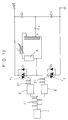
- a primary object of the present invention is to provide a light emitting power supply circuit capable of operating many types of loads and having high operating efficacy.
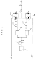
- FIG. 8 The aforementioned operating mode is shown in FIG. 8 in correspondence with the circuit shown in FIG. 1.
- Vf represents the voltage waveform of trigger pulses.
- the additional requirement: ⁇ 1 ⁇ ⁇ ⁇ ⁇ 0 is imposed on the inverter using FET switches.
- the present invention imposes no substantial limit on the pulse duration ⁇ of a pulse signal applied to the switch, and consequently, the luminance of lighted EL is more readily adjustable.
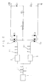
- FIG. 3 shows an exemplary EL light emitting power supply circuit according to the second aspect.
- the signals for turning ON (or opening) the zero-crossing switches T1, T2 in the EL light emitting power supply circuit according to the present invention may be optical signals and other conventionally used signals as well as the previously mentioned trigger voltage pulses. Description is made using the trigger voltage as typical signals.
- a pulse oscillator 1 produces pulse oscillation waves 11 alternately at a frequency f and a period of 2T which are separated into plus and minus pules by pulse selector circuits.
- a circuit (trigger circuit) on the side of a pulse oscillator 1 can be electrically isolated from a circuit (power circuit) on the side of EL so that the oscillator 1 and related components may be effectively protected.
- switches Tr1 and Tr2 may be used as the switches Tr1 and Tr2. Connection is made such that the photo-thyristor couplers PSC1, PSC2 controlledly open and close the switches Tr1, Tr2, respectively.
- photo-thyristor coupler PSC2 Upon subsequent receipt of an inverted pulse, photo-thyristor coupler PSC2 becomes conductive and the same as above is repeated on the opposite side channel.
- Such a zero-crossing circuit may be obtained by coupling a bipolar capacitor in parallel with R1, R2 because the circuit is only required to achieve the above-mentioned dynamism.
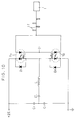
- FIGS. 12 and 13 illustrate preferred embodiments of the light emitting power supply circuit of the present invention in which the light emitting section comprises a load having resistance and/or diode characteristic.
- the light emitting power supply circuit shown in FIG. 12 is the same as the foregoing EL light emitting circuit except that an inductor L, a bipolar capacitor C7, and a load 4 are series connected to form a load circuit. Also, the light emitting power supply circuit using a transformer T shown in FIG. 13 is the same as the foregoing EL light emitting circuit except that the EL is replaced by a load 4. In this way, the foregoing light emitting circuits which have been described as having EL can be applied to loads having resistance and/or diode characteristic simply by replacing a part thereof.
- the load 4 in FIGS. 12 and 13 is replaced by a light emitting section having a combination of predetermined loads.
- the bipolar capacitor C7 may be eliminated from a light emitting circuit corresponding to FIG. 12 since the circuit has a capacitive component of EL.
- the light emitting section comprises an EL panel which is a preferred load having capacitive load characteristic.
- a DC power source of the single mode can be modified into a DC power source of the dual mode by using a pair of bipolar capacitors having substantially equal capacitance to divide the power source voltage.
- the pair of bipolar capacitors serve as reverse current buffers.
- the light emitting power supply circuit using an EL panel according to the invention is push-pull driven at a frequency f.
- f ranges from about 50 Hz to about 600 Hz
- EL has a capacitance of about 0.1 ⁇ F to about 10 ⁇ F
- L is about 30 mH to about 10 H.
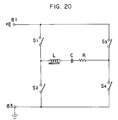
- the light emitting power supply circuit of the invention utilizes the transient current vibration phenomenon of an LC or LCR series circuit. The phenomenon is described in conjunction with FIGS. 16, 17, 18 and 19.
- the operating system using first and second inverters according to the present invention can use a single DC power source of the single mode of 50 to 75 V, which is quite beneficial in the construction of a DC-DC converter and power efficacy.
- the zero-crossing mechanism may comprises a zero-crossing switch element and/or a zero-crossing circuit as previously described.
- photocouplers such as photo-thyristor couplers as the zero-crossing mechanisms permits an oscillator section (trigger circuit) to be electrically isolated from a circuit (power circuit) on the EL side, thereby effectively protecting the oscillator section.
- charging current to EL flows through the thyristor and the reverse current flows through the reverse current bypass diode for feeding back and recovery.
- T0 is a time span between trigger pulses f1 and f2.
- the use of the light emitting power supply circuit of the present invention allows a load factor to be adjusted at a desired value by regulating or adjusting frequency f. This is readily understood from the waveform of current I in FIG. 8 because a higher frequency f results in a reduced width of ⁇ and a lower frequency f results in an extended width of ⁇ , but the waveform of current I through the load circuit for every half cycle (half period T0) remains unchanged.
- the remaining switch(es) may be comprised of a field effect transistor or another transistor whose channel is opened and closed in synchronization with the zero-crossing switch element(s).
- the switch turn-on time is from ⁇ to T0, a wide change of time constant ⁇ can be accommodated by setting or adjusting the turn-on time in the vicinity of T0.
- the oscillator circuit can be electrically isolated from the load circuit so that the oscillator circuit is effectively protected.
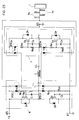
- FIG. 23 illustrates one preferred embodiment using such a zero-crossing circuit.
- switches S1, S2, S3, S4 constitute a main circuit for load current with reverse current bypass diodes D1, D2, D3, D4, an inductor L, and EL.
- the photo-thyristor couplers PSC1, PSC2, PSC3, PSC4, resistors R11, R12, R21, R22, R31, R32, R41, R42, bipolar capacitors C1, C2, C3, C4, inductor L, and EL constitute an ancillary or driving circuit for controlling the switches for opening and closing, part of the load current flowing through the ancillary circuit.
- the resistors R11, R12, R21, R22, R31, R32, R41, R42 in the ancillary circuit serve to limit the current flow through the ancillary circuit and to divide the potential across the ancillary circuit for delivering a gate voltage to the switches S1, S2, S3, S4.
- the bipolar capacitors C1, C2, C3, C4 serve to help drive the switches S1, S2, S3, S4 stably and may be commonly used ones.
- One of the important features of the light emitting power supply circuit of the present invention is to recover electric power to the supply power source side as reverse current. However, if it is undesirable to return the current directly to the power source, like the operating circuit using a single inverter, a buffer capacitor C5 is provided on the power source side as shown in FIG. 24 so that capacitor C5 is charged and discharged. If it is desirable to protect the power source, a reverse-blocking diode D5 may be provided.
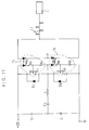
- This circuit is a modification of the foregoing embodiment wherein the inductor L is replaced by a transformer T and a bipolar capacitor C6 is provided in place of EL to form a primary side circuit whereby AC power available on the secondary side of the transformer T is used to operate EL.
- the embodiment is shown in FIG. 11 as having not only EL, but also a compensating inductor L' in series with the EL connected between output terminals of the transformer T on its secondary side.
- This circuit allows high AC voltage to be applied to the load EL.
- FIGS. 26 and 27 illustrate preferred embodiments of the light emitting power supply circuit of the present invention in which the light emitting section comprises a load having resistance and/or diode characteristic.
- the light emitting power supply circuit using a transformer T shown in FIG. 27 is the same as the foregoing EL operating circuit except that the EL is replaced by a load 3.
- the load circuit is provided with coupling terminals adapted for removably coupling to the light emitting section or load whereby the light emitting section or load can be removably coupled at the coupling terminals.
- an EL element having a varying surface area or a variety of loads can be operated at any desired level of lighting luminance with the same inverter, the operating system is substantially improved in mass production amenability and yield.
- the power source voltage may be one half of that required in the conventional design. This results in effective utilization of the power source voltage and is very advantageous in the manufacture of a converter for providing a DC power source.
- the inductor L was a shielded pot core of ferrite having a coil wound thereon. It had an inductance of 29.5 mH and a DC resistance of about 4 ⁇ .
- EL panel A dimensions 720 mm x 550 mm luminous area 3766.0 cm2
- EL panel B dimensions 550 mm x 550 mm luminous area 2851.4 cm2
- the EL panels were of green lighting type available from Fukubi Chemical K.K. and had a sheet resistivity of about 80 ⁇ .
- the EL light emitting power supply circuit of the present invention achieves EL operation at an efficacy of about 3 to 4 lumen/watt, which is improved by a factor of 3 or 4 over the conventional techniques.
- Heat release was little as evidenced by the fact that the luminous surface temperature relative to the ambient atmosphere marked an increase of less than 1 degree after 8 hours of operation.
- the EL panels were of green lighting type available from Fukubi Chemical K.K. and identified below as A1, A2, B1, B2, C, D1, D1, D2, E, F and G. For each type, a plurality of panels having different sheet resistivity were prepared.
- EL panel A1 luminous area 3766.0 cm2
- EL panel A2 luminous area 3766.0 cm2
- EL panel B1 luminous area 2851.4 cm2
- EL panel B2 luminous area 2851.4 cm2
- EL panel C luminous area 1367.4 cm2
- EL panel D2 luminous area 2044.4 cm2
- EL panel E luminous area 1094.4 cm2
- EL panel F luminous area 678.4 cm2
- EL panel G luminous area 528.0 cm2
- the inductor L had an inductance of 30 mH, and the inverter was connected across an input power source of ⁇ 50 volts which had been increased by a DC-DC converter of the dual mode.
- Table 2 shows the adjusted operating frequency for operating sets of A1 + A1, B1 + B1, A2, D1 + E, B2, D2, C, F, and G at the same illuminance of 10 lx.
- Table 2 also reported in Table 2 is the R equivalent component in the circuit including the EL panel's sheet resistivity.
- Table 2 Set Luminous area (cm2) Operating frequency (Hz) at R equivalent component of 40 ⁇ 50 ⁇ 60 ⁇ 70 ⁇ 80 ⁇ 90 ⁇ 100 ⁇ G 528.0 80 83 87 91 96 101 106 F 678.4 82 86 91 96 102 108 114 C 1367.4 90 96 105 113 123 134 147 D2 2044.4 96 106 117 129 144 161 182 B2 2851.4 103 116 131 148 170 197 230 D1+E 3138.8 105 119 135 155 180 211 250 A2 3766.0 110 126 146 171 203 244 B1+B1 5702.8 125 150 182 226 A1+A1 7532.0 139 173 221
- the system of the present invention allows a single EL operating power supply circuit, that is, a single EL operating device to operate various sets of EL panels having different surface area or different sheet resistivity including from (A1 + A1) to G at a desired level of illuminance simply by regulating the frequency.
- the EL operating efficacy was about 3 to 4 lumen/watt. In the prior art, the EL operating efficacy was less than 1 lumen/watt.
Landscapes
- Physics & Mathematics (AREA)
- Engineering & Computer Science (AREA)
- Microelectronics & Electronic Packaging (AREA)
- Optics & Photonics (AREA)
- Electroluminescent Light Sources (AREA)
Abstract
Applications Claiming Priority (4)
| Application Number | Priority Date | Filing Date | Title |
|---|---|---|---|
| JP2027873A JPH04298988A (ja) | 1990-02-07 | 1990-02-07 | El発光電源回路およびel用電源回路 |
| JP27873/90 | 1990-02-07 | ||
| JP59138/90 | 1990-03-09 | ||
| JP2059138A JPH0549265A (ja) | 1989-11-30 | 1990-03-09 | 負荷電源回路、負荷駆動用電源回路および負荷交流駆動方法 |
Publications (2)
| Publication Number | Publication Date |
|---|---|
| EP0487732A1 true EP0487732A1 (fr) | 1992-06-03 |
| EP0487732A4 EP0487732A4 (en) | 1993-03-10 |
Family
ID=26365866
Family Applications (1)
| Application Number | Title | Priority Date | Filing Date |
|---|---|---|---|
| EP19910903281 Withdrawn EP0487732A4 (en) | 1990-02-07 | 1991-02-07 | Light-emitting power source circuit |
Country Status (3)
| Country | Link |
|---|---|
| US (1) | US5323305A (fr) |
| EP (1) | EP0487732A4 (fr) |
| WO (1) | WO1991012703A1 (fr) |
Cited By (3)
| Publication number | Priority date | Publication date | Assignee | Title |
|---|---|---|---|---|
| EP0699015A1 (fr) * | 1994-08-24 | 1996-02-28 | Hewlett-Packard Company | Circuit d'alimentation à récupération de l'énergie pour un dispositif électroluminescent |
| WO2003019987A1 (fr) * | 2001-08-23 | 2003-03-06 | Mark Purcell | Circuit de commande de charge capacitive |
| EP1417867A4 (fr) * | 2001-02-20 | 2004-07-28 | Durel Corp | Onduleur permettant de commander une lampe et des diodes electroluminescentes |
Families Citing this family (49)
| Publication number | Priority date | Publication date | Assignee | Title |
|---|---|---|---|---|
| DE4111581A1 (de) * | 1991-04-10 | 1992-10-15 | Diehl Gmbh & Co | Inverterschalter fuer eine kapazitive lichtquelle |
| JP2843191B2 (ja) * | 1992-01-30 | 1999-01-06 | 富士通株式会社 | 電子デバイスの駆動回路 |
| JP3378599B2 (ja) | 1992-10-30 | 2003-02-17 | 田淵電機株式会社 | El駆動回路 |
| US5457359A (en) * | 1993-08-06 | 1995-10-10 | Olin Corporation | Control for electroluminescent loads |
| US5568016A (en) * | 1994-10-18 | 1996-10-22 | Norand Corporation | Power supply for an electroluminescent panel or the like |
| US5747938A (en) * | 1994-10-18 | 1998-05-05 | Norand Corporation | Automatic control electroluminescent backlight panel |
| US5936599A (en) * | 1995-01-27 | 1999-08-10 | Reymond; Welles | AC powered light emitting diode array circuits for use in traffic signal displays |
| US5557175A (en) * | 1995-06-13 | 1996-09-17 | Harris Corporation | Battery operated inverter circuit for capacitive loads such as electroluminescent lamps |
| US5525869A (en) * | 1995-06-15 | 1996-06-11 | Harris Corporation | Efficient battery operated inverter circuit for capacitive loads such as electroluminescent lamps |
| US5733288A (en) * | 1995-07-18 | 1998-03-31 | Cohort Medical Products Group, Inc. | Bone brush |
| JPH1020274A (ja) * | 1996-07-05 | 1998-01-23 | Fujitsu Ltd | 液晶表示駆動回路及び液晶表示装置 |
| US6570505B1 (en) | 1997-12-30 | 2003-05-27 | Gelcore Llc | LED lamp with a fault-indicating impedance-changing circuit |
| US7066628B2 (en) * | 2001-03-29 | 2006-06-27 | Fiber Optic Designs, Inc. | Jacketed LED assemblies and light strings containing same |
| US7931390B2 (en) * | 1999-02-12 | 2011-04-26 | Fiber Optic Designs, Inc. | Jacketed LED assemblies and light strings containing same |
| US6181589B1 (en) * | 1999-07-02 | 2001-01-30 | Durel Corporation | Half-bridge inverter for coupling an EL lamp to a high voltage DC rail |
| US6285139B1 (en) | 1999-12-23 | 2001-09-04 | Gelcore, Llc | Non-linear light-emitting load current control |
| US7296753B1 (en) * | 2000-01-14 | 2007-11-20 | Bae Systems Information And Electronic Systems Integration Inc. | Isolated control apparatus incorporating light controlled power semiconductors |
| DE20024002U1 (de) * | 2000-03-17 | 2009-03-26 | Tridonicatco Gmbh & Co. Kg | Spannungsversorgung von Leuchtdioden (LEDs) |
| US6366063B1 (en) * | 2000-03-22 | 2002-04-02 | Nec Corporation | Circuit and method for driving capacitive load |
| KR100564138B1 (ko) * | 2001-07-31 | 2006-03-27 | 주식회사 레다트 | 듀얼전압 전원공급장치 |
| US6853150B2 (en) * | 2001-12-28 | 2005-02-08 | Koninklijke Philips Electronics N.V. | Light emitting diode driver |
| WO2005017852A2 (fr) * | 2003-08-01 | 2005-02-24 | Bae Systems | Appareil de commande isole equipe de semi-conducteurs de puissance a commande optique |
| US7850362B2 (en) * | 2004-11-10 | 2010-12-14 | 1 Energy Solutions, Inc. | Removable LED lamp holder with socket |
| US7850361B2 (en) * | 2004-11-10 | 2010-12-14 | 1 Energy Solutions, Inc. | Removable LED lamp holder |
| US8016440B2 (en) * | 2005-02-14 | 2011-09-13 | 1 Energy Solutions, Inc. | Interchangeable LED bulbs |
| US20070025109A1 (en) | 2005-07-26 | 2007-02-01 | Yu Jing J | C7, C9 LED bulb and embedded PCB circuit board |
| US7265496B2 (en) * | 2005-09-23 | 2007-09-04 | Fiber Optic Designs, Inc. | Junction circuit for LED lighting chain |
| US7276858B2 (en) | 2005-10-28 | 2007-10-02 | Fiber Optic Designs, Inc. | Decorative lighting string with stacked rectification |
| US7250730B1 (en) * | 2006-01-17 | 2007-07-31 | Fiber Optic Designs, Inc. | Unique lighting string rectification |
| US8083393B2 (en) | 2006-02-09 | 2011-12-27 | 1 Energy Solutions, Inc. | Substantially inseparable LED lamp assembly |
| JP5148515B2 (ja) * | 2006-03-06 | 2013-02-20 | コーニンクレッカ フィリップス エレクトロニクス エヌ ヴィ | 供給回路及び供給回路を有する装置 |
| US8154898B2 (en) * | 2006-06-15 | 2012-04-10 | Supertex, Inc. | Current driven bipolar high voltage driver for capacitive loads |
| US7963670B2 (en) * | 2006-07-31 | 2011-06-21 | 1 Energy Solutions, Inc. | Bypass components in series wired LED light strings |
| US20080025024A1 (en) * | 2006-07-31 | 2008-01-31 | Jingjing Yu | Parallel-series led light string |
| US7784993B2 (en) | 2007-07-13 | 2010-08-31 | 1 Energy Solutions, Inc. | Watertight LED lamp |
| US7883261B2 (en) * | 2008-04-08 | 2011-02-08 | 1 Energy Solutions, Inc. | Water-resistant and replaceable LED lamps |
| US8376606B2 (en) * | 2008-04-08 | 2013-02-19 | 1 Energy Solutions, Inc. | Water resistant and replaceable LED lamps for light strings |
| US8314564B2 (en) | 2008-11-04 | 2012-11-20 | 1 Energy Solutions, Inc. | Capacitive full-wave circuit for LED light strings |
| WO2010088954A1 (fr) * | 2009-02-04 | 2010-08-12 | Osram Gesellschaft mit beschränkter Haftung | Circuiterie et procédé pour faire fonctionner une feuille électroluminescente |
| CN201391793Y (zh) * | 2009-04-20 | 2010-01-27 | 喻北京 | Led灯泡的新型散热结构 |
| US20100289566A1 (en) * | 2009-05-14 | 2010-11-18 | Jimmy Ko | Amplitude AC noise filter with universal IEC connection |
| US8836224B2 (en) * | 2009-08-26 | 2014-09-16 | 1 Energy Solutions, Inc. | Compact converter plug for LED light strings |
| US20130033850A1 (en) * | 2011-08-02 | 2013-02-07 | Vivian Fan | LED Light Bar and Display Device Using the Same |
| US11025345B2 (en) | 2013-09-19 | 2021-06-01 | Radius Universal Llc | Hybrid cable providing data transmission through fiber optic cable and low voltage power over copper wire |
| US12368615B2 (en) | 2013-09-19 | 2025-07-22 | Radius Universal Llc | Fiber optic communications and power network |
| US10855381B2 (en) * | 2013-09-19 | 2020-12-01 | Radius Universal Llc | Fiber optic communications and power network |
| US10277330B2 (en) | 2013-09-19 | 2019-04-30 | Radius Universal Llc | Fiber optic communications and power network |
| FR3072520B1 (fr) | 2017-10-16 | 2020-09-04 | St Microelectronics Tours Sas | Circuit de commande d'un thyristor ou triac |
| CN117643177A (zh) | 2021-06-29 | 2024-03-01 | 昕诺飞控股有限公司 | 对反并联激光二极管和led的串进行hf ac驱动 |
Family Cites Families (14)
| Publication number | Priority date | Publication date | Assignee | Title |
|---|---|---|---|---|
| JPS5913748B2 (ja) * | 1977-06-28 | 1984-03-31 | 日本電信電話株式会社 | 容量性表示素子の駆動回路 |
| US4253097A (en) * | 1979-03-29 | 1981-02-24 | Timex Corporation | Method and apparatus for reducing power consumption to activate electroluminescent panels |
| US4346332A (en) * | 1980-08-14 | 1982-08-24 | General Electric Company | Frequency shift inverter for variable power control |
| JPS59152692A (ja) * | 1983-02-21 | 1984-08-31 | イビデン株式会社 | 多元的に組み立てられたプリント配線基板 |
| JPS59152692U (ja) * | 1983-03-31 | 1984-10-13 | 東芝ライテック株式会社 | Elランプ点灯装置 |
| JPS61133600A (ja) * | 1984-12-01 | 1986-06-20 | Toshiba Corp | X線装置 |
| JPS6249832A (ja) * | 1985-08-30 | 1987-03-04 | 株式会社東芝 | 画像処理装置 |
| CA1292770C (fr) * | 1986-07-30 | 1991-12-03 | Kenneth Lipman | Dispositif et methode de commande pour inverseur commute par une force |
| JPS63138691A (ja) * | 1986-12-01 | 1988-06-10 | キヤノン株式会社 | エレクトロルミネツセンス素子駆動回路 |
| JPS63202888A (ja) * | 1987-02-13 | 1988-08-22 | インターナシヨナル・ビジネス・マシーンズ・コーポレーシヨン | 電界発光パネル用の電源回路 |
| US4833584A (en) * | 1987-10-16 | 1989-05-23 | Wisconsin Alumni Research Foundation | Quasi-resonant current mode static power conversion method and apparatus |
| US5027040A (en) * | 1988-09-14 | 1991-06-25 | Daichi Company, Ltd. | EL operating power supply circuit |
| DE69015418T2 (de) * | 1989-04-25 | 1995-05-04 | Matsushita Electric Works Ltd | Energieversorgung. |
| US5066895A (en) * | 1989-10-20 | 1991-11-19 | Alrit Corporation | Electroluminescent lamp driver |
-
1991
- 1991-02-07 US US07/768,847 patent/US5323305A/en not_active Expired - Fee Related
- 1991-02-07 WO PCT/JP1991/000151 patent/WO1991012703A1/fr not_active Ceased
- 1991-02-07 EP EP19910903281 patent/EP0487732A4/en not_active Withdrawn
Cited By (4)
| Publication number | Priority date | Publication date | Assignee | Title |
|---|---|---|---|---|
| EP0699015A1 (fr) * | 1994-08-24 | 1996-02-28 | Hewlett-Packard Company | Circuit d'alimentation à récupération de l'énergie pour un dispositif électroluminescent |
| US5559402A (en) * | 1994-08-24 | 1996-09-24 | Hewlett-Packard Company | Power circuit with energy recovery for driving an electroluminescent device |
| EP1417867A4 (fr) * | 2001-02-20 | 2004-07-28 | Durel Corp | Onduleur permettant de commander une lampe et des diodes electroluminescentes |
| WO2003019987A1 (fr) * | 2001-08-23 | 2003-03-06 | Mark Purcell | Circuit de commande de charge capacitive |
Also Published As
| Publication number | Publication date |
|---|---|
| US5323305A (en) | 1994-06-21 |
| EP0487732A4 (en) | 1993-03-10 |
| WO1991012703A1 (fr) | 1991-08-22 |
Similar Documents
| Publication | Publication Date | Title |
|---|---|---|
| EP0487732A1 (fr) | Circuit d'alimentation luminescent | |
| US5027040A (en) | EL operating power supply circuit | |
| US6043610A (en) | Battery operated power supply including a low level boost and a high level boost | |
| US4388563A (en) | Solid-state fluorescent lamp ballast | |
| US8203283B2 (en) | Light emitting diode (LED) arrangement with bypass driving | |
| US6043609A (en) | Control circuit and method for illuminating an electroluminescent panel | |
| TW200524481A (en) | Current-mode driver | |
| US4319164A (en) | Power factor compensating electroluminescent lamp DC/AC inverter | |
| JPH0654528A (ja) | ゼロボルトスイッチングパワーコンバータのパワースイッチのためのドライブ回路 | |
| US4099099A (en) | Method of and switching device for reducing feedback from a consumer periodically connected to an A.C. line | |
| GB2431298A (en) | Series resonant dc-dc converter | |
| US6124680A (en) | Lighting device for illumination and lamp provided with the same | |
| CN101347047B (zh) | 用于驱动发光二极管单元的装置 | |
| US4417153A (en) | High frequency switching circuit | |
| US6414448B1 (en) | Electronic ballast for a gas discharge lamp | |
| US20070085492A1 (en) | Matrix inverter for driving multiple discharge lamps | |
| US6208086B1 (en) | Halogen power converter with complementary switches | |
| JPS6412865A (en) | Snubber circuit | |
| JPWO1991012704A1 (ja) | 照明器具故障部位集中表示装置及び故障情報収集方法 | |
| JPWO1991012703A1 (ja) | 発光電源回路 | |
| JP2737391B2 (ja) | リンギングチョークコンバータ | |
| JPH04298988A (ja) | El発光電源回路およびel用電源回路 | |
| JP2934649B2 (ja) | El素子の駆動装置 | |
| Boonyaroonate et al. | Half-bridge inverter using hysteresis current control for electroluminescent lamp | |
| SU1529193A1 (ru) | Ключевой регул тор напр жени |
Legal Events
| Date | Code | Title | Description |
|---|---|---|---|
| PUAI | Public reference made under article 153(3) epc to a published international application that has entered the european phase |
Free format text: ORIGINAL CODE: 0009012 |
|
| 17P | Request for examination filed |
Effective date: 19920224 |
|
| AK | Designated contracting states |
Kind code of ref document: A1 Designated state(s): BE DE ES FR GB IT NL |
|
| A4 | Supplementary search report drawn up and despatched |
Effective date: 19930119 |
|
| AK | Designated contracting states |
Kind code of ref document: A4 Designated state(s): BE DE ES FR GB IT NL |
|
| 17Q | First examination report despatched |
Effective date: 19950123 |
|
| GRAG | Despatch of communication of intention to grant |
Free format text: ORIGINAL CODE: EPIDOS AGRA |
|
| STAA | Information on the status of an ep patent application or granted ep patent |
Free format text: STATUS: THE APPLICATION HAS BEEN WITHDRAWN |
|
| 18W | Application withdrawn |
Withdrawal date: 19961028 |