EP0487917A2 - Circuits ECL/NTL à faible consommation et grande vitesse - Google Patents
Circuits ECL/NTL à faible consommation et grande vitesse Download PDFInfo
- Publication number
- EP0487917A2 EP0487917A2 EP91118486A EP91118486A EP0487917A2 EP 0487917 A2 EP0487917 A2 EP 0487917A2 EP 91118486 A EP91118486 A EP 91118486A EP 91118486 A EP91118486 A EP 91118486A EP 0487917 A2 EP0487917 A2 EP 0487917A2
- Authority
- EP
- European Patent Office
- Prior art keywords
- transistor
- circuit
- pull
- terminal connected
- complementary
- Prior art date
- Legal status (The legal status is an assumption and is not a legal conclusion. Google has not performed a legal analysis and makes no representation as to the accuracy of the status listed.)
- Withdrawn
Links
- 230000000295 complement effect Effects 0.000 claims abstract description 34
- 230000001052 transient effect Effects 0.000 claims abstract description 18
- 238000010168 coupling process Methods 0.000 claims abstract description 6
- 238000005859 coupling reaction Methods 0.000 claims abstract description 6
- 230000008878 coupling Effects 0.000 claims abstract description 5
- 239000003990 capacitor Substances 0.000 claims description 25
- 238000009877 rendering Methods 0.000 claims 1
- 238000010586 diagram Methods 0.000 description 8
- 230000000593 degrading effect Effects 0.000 description 4
- 230000006872 improvement Effects 0.000 description 4
- 230000007704 transition Effects 0.000 description 4
- 230000008901 benefit Effects 0.000 description 2
- 244000309464 bull Species 0.000 description 1
- 230000001419 dependent effect Effects 0.000 description 1
- 238000007599 discharging Methods 0.000 description 1
- 230000009467 reduction Effects 0.000 description 1
- 230000000630 rising effect Effects 0.000 description 1
Images

Classifications
-
- H—ELECTRICITY
- H03—ELECTRONIC CIRCUITRY
- H03K—PULSE TECHNIQUE
- H03K19/00—Logic circuits, i.e. having at least two inputs acting on one output; Inverting circuits
- H03K19/02—Logic circuits, i.e. having at least two inputs acting on one output; Inverting circuits using specified components
- H03K19/08—Logic circuits, i.e. having at least two inputs acting on one output; Inverting circuits using specified components using semiconductor devices
- H03K19/082—Logic circuits, i.e. having at least two inputs acting on one output; Inverting circuits using specified components using semiconductor devices using bipolar transistors
- H03K19/086—Emitter coupled logic
-
- H—ELECTRICITY
- H03—ELECTRONIC CIRCUITRY
- H03K—PULSE TECHNIQUE
- H03K19/00—Logic circuits, i.e. having at least two inputs acting on one output; Inverting circuits
- H03K19/01—Modifications for accelerating switching
- H03K19/013—Modifications for accelerating switching in bipolar transistor circuits
- H03K19/0136—Modifications for accelerating switching in bipolar transistor circuits by means of a pull-up or down element
Definitions
- the present invention relates generally to bipolar transistor logic circuits, and more particularly, to emitter coupled logic (ECL) and non-threshold logic (NTL) circuits wherein the dc power dissipation and switching current are greatly reduced by utilizing an ac-coupled complementary push-pull output stage.
- ECL emitter coupled logic
- NTL non-threshold logic
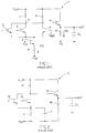
- Fig. 1 is a schematic diagram of a conventional ECL circuit 1.
- the input signal is applied to the bases of transistors 2 and 3 which are differentially coupled to transistor 4. Since the output is taken from node A, the output will perform a NOR function of the input signals.
- the base of transistor 4 is tied to a reference voltage V REF which is equal to the median between the logical high voltage and the logical low voltage of the integrated circuit 1.
- Transistor 5 and resistor 9 provide a current source for differential transistors 2, 3 and 4.
- transistor 3 When the input signal to the base of transistor 3 is a logical low voltage, transistor 3 is off, and transistor 4 is on. The current provided by transistor 5 and resistor 9 flows through transistor 4. The voltage at node A is high. The output is taken from node A through transistor 6 which is connected in an emitter follower configuration. Thus, the output will be a high output voltage.
- transistor 3 When the input rises from a logical low voltage to a logical high voltage, transistor 3 will switch on and transistor 4 will switch off once the input signal crosses V REF . As transistor 3 switches on, node A will fall from a high voltage to a low voltage pulling the base of transistor 6 low and providing a low output voltage.
- the output is pulled down from a high output voltage to a low output voltage through resistor 10 to discharge the load capacitor C L .
- Load capacitor C L consists of the capacitances of any driven gates and wiring capacitance.
- the time required to pull down the output is determined by the time required for the input signal to rise from a logical low voltage to V REF , the time required to pull down the voltage at node A, and the time needed to discharge capacitor C L from a high output voltage to a low output voltage through resistor 10. The latter time is determined by a time constant which is obtained by multiplying the resistance of resistor 10 by the capacitance of capacitor C L .
- resistor 10 in order to achieve a fast pull-down, resistor 10 must be as low as possible. However, this results in a higher dc current I EF and, thus, higher power dissipation.
- the dc current I EF during stand-by and during switching is the same which results in high dc power dissipation.
- ECL circuit 1 When the input switches from a logical high voltage to a logical low voltage, transistor 3 will switch off, and transistor 4 will switch on. The base of transistor 6 is pulled high through resistor 7 thereby turning transistor 6 on strongly to charge the output node and provide a high output voltage.
- ECL circuit 1 is limited in its operation when pulling up the output by the need to provide the drive current for transistor 6 through resistor 7.
- ECL circuit 1 is further limited in that the switching current I CS is the same whether it is flowing through resistor 7 and transistor 3 or through resistor 8 and transistor 4 because the current source, transistor 5 and and resistor 9, supplies the same I CS regardless of which differential transistor is on. Thus, resistor 7 and resistor 8 have the same resistance values.
- the time required to pull up the output is determined by the time required for the input signal to fall from a logical high voltage to V REF , the time required to pull up the voltage at node A through resistor 7 which determines the time needed to charge capacitor C L from a low output voltage to a high output voltage through emitter follower transistor 6. Therefore, in order to achieve a fast pull-up of the voltage at node A, resistor 7, and thus resistor 8, must be selected as low as possible.
- the switching current I CS is inversely proportional to resistors 7 and 8 for a fixed voltage swing. Thus, a small value for resistors 7 and 8 will result in a large switching current I CS .
- the pull-down delay is limited by resistor 10.
- high speed operation means a small resistor value for resistor 10 and high dc current I EF .
- the pull-up delay is limited by resistors 7 and 8.
- a fast pull-up means small resistors 7 and 8 and a large switch current I CS .
- the base of the pull-down transistor is biased to maintain a low steady state current.
- node A will fall from a high voltage level to a low voltage level and emitter follower transistor 6 is cutoff.
- the voltage at the collector of transistor 4 rises from a low voltage level to a high voltage level, and this signal is ac-coupled to the base of the pull-down transistor.
- the coupling capacitor couples a transient voltage pulse to the base of the pull-down transistor, thereby turning on the pull-down transistor strongly and briefly to provide a large transient pull-down current.
- a small emitter follower current I EF can be used while still maintaining a fast pull-down.
- the pull-up transistor is turned off momentarily, thus, further improving the pull-down delay.
- the APD-ECL is faster, and the output transition from a high output voltage to a low output voltage is steeper than the discharge through resistor 10 in conventional ECL circuit 1. This is because the current used to discharge capacitor C L is supplied by the pull-down transistor which has a much smaller time constant than the passive pull-down in circuit 1.
- the power dissipation in the emitter follower stage of the APD-ECL is much less than that of circuit 1 because the dc current in the output stage is small during stand-by and momentarily raised up during switching, whereas in circuit 1, I EF is at the same value during stand-by and when circuit 1 switches.
- a secondary advantage of the APD-ECL circuit stems from the fact that the steady state current through the emitter follower transistor 6 is low, and therefore, the output high voltage is approximately 100 mV closer to V CC than in conventional ECL circuit 1. Thus, a lower V CC may be used which further reduces the dc power dissipation in the APD-ECL circuit.
- APD-ECL circuit is an improvement over conventional ECL circuit 1, the former circuit does not overcome the second problem stated above.
- a large switching current I CS is still necessary to achieve fast switching of the logic stage, especially for the pull-up which is still limited by pull-up resistors 7 and 8.
- Fig. 2 is a schematic diagram of a conventional non-threshold logic (NTL) circuit 11.
- NTL circuit 11 The operation and power/speed performance of conventional NTL circuit 11 is similar to that described above for ECL circuit 1 except for the differences discussed below.
- NTL circuit 11 there is no reference transistor differentially coupled to the input transistors 12 and 13, and as a result, the voltage at the base of the emitter follower transistor 14 will immediately rise or fall when the input falls or rises.
- the delay component in ECL circuit 1 attributable to the time it takes for the input signal to rise to V REF during pull-up is not present in NTL circuit 11.
- NTL circuit can be operated with a lower power supply than conventional ECL circuit 1, and therefore, dissipates less dc power than ECL circuit 1.
- ECL circuit 1 The two problems present in ECL circuit 1 are also present in conventional NTL circuit 1: (1) the pull-down delay is limited by resistor 18. Thus, high speed operation means a small resistor value for resistor 18 and high dc current I EF . (2) The pull-up delay is limited by pull-up resistor 15. Thus, a fast pull-up means a small pull-up resistor 15 and a large switch current I CS .
- a circuit which has been developed to overcome the first problem in NTL circuit 1 is described in M. Usami and N. Shiozawa, "SPL (Super Push-Pull Logic) A Bipolar Novel Low-Power High-Speed Logic Circuit," Dig. of Tech. Papers, Symp. on VLSI Cirs., 11-12, May, 1989.
- the SPL circuit is similar in operation to the APD-ECL in that the SPL circuit reduces dc power dissipation by utilizing an ac-coupled active pull-down transistor.
- the base of a pull-down transistor is ac-coupled to the emitter(s) of the input transistors via a capacitor.
- the collector of the pull-down transistor is coupled to the emitter of the output emitter follower transistor 14 and to the output node and the emitter of the pull-down transistor is returned to V EE .
- the capacitor couples a transient voltage pulse to the base of the pull-down transistor, thereby turning on the pull-down transistor providing a large transient pull-down current.
- the SPL circuit does not overcome the second problem stated above. A large switching current I CS is still necessary to achieve fast switching of the logic stage, especially for the pull-up which is still limited by pull-up resistor 15.
- the present invention is directed to ECL and NTL circuits with an ac-coupled complementary push-pull output stage which enables the circuits to operate at high speeds with minimum dc power dissipation and small switching current I CS .
- the present ECL circuit has multiple input transistors which are differentially coupled to a reference transistor.
- the switching current I CS is drawn from the common emitter node and the signal at the common collector node of the input transistors is applied to the base of an emitter follower transistor.
- the output is taken from the emitter of the emitter follower transistor which is connected to the common collector node of a pair of complementary push-pull (PNP-NPN) transistors.
- a biasing means is provided in order to bias the complementary transistors at cut-in ('NEARLY ON') condition and maintain a low stand-by current at the output stage.
- a pulse coupling means which is connected between the common emitter node of the input transistors and the bases of the complementary transistors, is used to apply a transient voltage pulse derived from a replica of an input signal to said bases to momentarily render one complementary transistor heavily conductive and turn the other one off. This will result in a large transient current flow in the conductive transistor thereby providing a fast pull-up or pull-down of the voltage at the output node.
- the voltage at the common emitter node of the input transistors immediately follows and oppositely directed pulses are applied to the complementary push-pull transistors via the two capacitors. This will switch the pull-up PNP transistor heavily on and the pull-down NPN transistor off quickly and momentarily, thereby providing a large transient pull-up current.
- a small amount of pull-up current is also supplied by the output emitter follower transistor.
- the pull-up current is mostly supplied by the pull-up PNP transistor and only a small fraction is supplied by the output emitter follower transistor.
- the pull-up delay is no longer dependent on the pull-up resistors.
- the pull-up resistors are used merely for setting the output logic levels through the emitter follower transistor.
- the present ECL circuit can be operated with less dc power dissipation and a lower switching current I CS than the conventional ECL and APD-ECL circuits.
- the operation and improvements in power dissipation, speed and switching current of the ac-coupled complementary push-pull ECL circuit are equally applicable to the disclosed ac-coupled complementary push-pull NTL circuit.
- the disclosed NTL circuit can be operated with less dc power dissipation and a lower switching current than the conventional NTL and SPL circuits.
- Fig. 3 is a schematic diagram of an ECL circuit 19 which utilizes an ac-coupled complementary push-pull output stage.
- the ECL circuit 19 improves the power/speed performance of ECL circuitry by allowing a very low switching current I CS to be used for the logic (current switch) stage to maintain the proper logic levels while eliminating the impact on the switching speed by the large pull-up resistors 27 and 28 of the logic stage.
- ECL circuit 19 includes a plurality of NPN bipolar transistors 20-25 and one PNP bipolar transistor 26. ECL circuit 19 is designed to be operated with two or three voltage levels supplied. The current trend in ECL circuitry is to use three voltage levels. The first level is V CC , the second level is V T which is at a lower voltage than V CC and the third level is V EE which is at a lower voltage than V T . ECL circuit 19 also includes at least one input transistor 21 which is differentially coupled to reference transistor 22. Additional input transistors can be connected in parallel with input transistor 21 as shown by transistor 20. Transistor 23 and resistor 29 provide switching current I CS to differential transistors 21 and 22.
- the base of transistor 22 is tied to a reference voltage V REF which is equal to the median between the logical high voltage and logical low voltage of ECL circuit 19.
- V REF reference voltage
- a power supply V CC is connected to the collector of transistor 21 via resistor 27 and the collector of transistor 22 via resistor 28.
- Transistor 24 is connected in an emitter-follower configuration wherein the base of transistor 24 is connected to the collector of transistor 21, and the emitter of transistor 24 is connected to the output.
- the collector of transistor 24 is directly connected to the power supply V CC .
- ECL circuit 19 further includes a biasing circuit which consists of resistors 30, 32 and 33 and diode 31. The biasing circuit is used to bias transistors 25 and 26 at cut-in ('NEARLY ON') condition, thereby establishing a stand-by current in transistors 25 and 26.
- transistor 21 When the input signal falls from a logical high to a logical low, transistor 21 will be switched off and transistor 22 will be switched on. Thus, the switching current I CS supplied by transistor 23 and resistor 29 will be switched from transistor 21 to transistor 22.
- the voltage at node B will rise from a low voltage to a high voltage. Since the output is taken from the emitter of transistor 24, the output voltage will rise from a low output voltage to a high output voltage.
- the voltage at common emitter node C will immediately follow the input signal until the input crosses V REF and at that point will remain at V REF minus the base to emitter voltage of transistor 22 V BE22 .
- the signal at node C will be a replica of the input signal in that when a logical high is at the input, the voltage at node C will equal the logical high voltage minus V BE21 and when the input is a logical low, the voltage at node C will equal V REF minus V BE22 .
- Transistors 25 and 26 are biased at cut-in condition by resistors 30, 32, and 33 and diode 31 to maintain a low stand-by current in transistors 25 and 26.
- the voltage signal at common emitter node C is ac-coupled to the bases of the complementary push-pull transistors 25 and 26 via capacitors 34 and 35, respectively.
- Capacitors 34 and 35 will couple a negative voltage pulse derived from a replica of the input signal to the bases of transistors 25 and 26, thereby turning off pull-down NPN transistor 25 and turning on pull-up PNP transistor 26 quickly and momentarily, providing a large transient pull-up current I P1 . Transistors 25 and 26 will then quickly return to stand-by condition.
- resistor 27 is no longer in the pull-up delay path as in conventional ECL circuit 1 and the APD-ECL circuit. Resistors 27 and 28 will have the same resistance values because the switching current I CS is the same regardless of whether it is flowing through resistor 27 and transistor 21 or through resistor 28 and transistor 22.
- Resistors 27 and 28 are used merely for setting the output logic levels through the emitter follower transistor 24. Large resistances can be used for resistors 27 and 28, and thus a small switching current I CS can now be used without degrading the speed.
- the dc power dissipation of ECL circuit 19 is much less than the conventional ECL and APD-ECL circuits because a lower switching current I CS can now be used while still achieving fast switching of the logic stage.
- Capacitors 34 and 35 will couple a positive voltage pulse derived from the replica signal to the bases of transistors 25 and 26, thereby heavily turning on pull-down NPN transistor 25 and turning off pull-up PNP transistor 26 quickly and momentarily, providing a large transient pull-down current I N1 to quickly discharge the output node.
- the pull-down delay of ECL circuit 19 is still longer than the pull-up delay as in the APD-ECL circuit. This is because when the input rises from a logical low to a logical high, the voltage at common emitter node C will follow only after the input crosses the reference voltage V REF whereas when the input falls from a logical high to a logical low, the voltage at common emitter node C follows the input immediately. Note that for conventional ECL circuit 1, the switching of the current will not occur until the input crosses the reference voltage in both transitions.
- circuit 19 The power supplies and input/output voltage levels of circuit 19 are compatible with conventional ECL circuits and, thus, can be mixed with conventional ECL circuits on the same chip.
- Fig. 4 is a schematic diagram of an NTL circuit 36 which utilizes an ac-coupled complementary push-pull output stage.
- NTL circuit 36 improves the power/speed performance of NTL circuitry by allowing a very low switch current to be used for the logic stage to maintain the proper logic levels while eliminating the impact on the switching speed by pull-up resistor 43 of the logic stage.
- NTL circuit 39 includes a plurality of NPN bipolar transistors 37-40 and one PNP bipolar transistor 41.
- NTL circuit 36 is designed to be operated with two or three voltage levels supplied. The current trend in NTL circuitry is to use three voltage levels. The first voltage source is V CC , the second level is V T which is at a lower voltage than V CC and the third level is V EE which is at a lower voltage than V T .
- NTL circuit 36 includes at least one input transistor 38. Additional input transistors can be connected in parallel with input transistor 38 as shown by transistor 37. The output performs a NOR function of the input signals.
- AC-coupling means are provided by capacitors 44 and 45 which are connected to the bases of complementary push-pull transistors 40 and 41.
- NTL circuit 36 also includes a biasing circuit which consists of resistors 46, 47, and 49 and diode 48.
- the biasing circuit is used to bias transistors 40 and 41 at cut-in condition, thereby establishing a stand-by current in transistors 40 and 41.
- NTL circuit 36 achieves a reduction in dc power dissipation and switching current without degrading the speed.
- the characteristics and power/speed performance of the NTL circuit 36 are similar to that of ECL circuit 19 except for the differences which will be discussed below in connection with the operation of NTL circuit 36.
- the voltage at node E When the input signal falls from a logical high to a logical low, the voltage at node E will immediately follow.
- the voltage signal at node E is ac-coupled to the bases of transistors 40 and 41 via capacitors 44 and 45, respectively.
- Capacitors 44 and 45 will couple a negative voltage pulse to the bases of transistors 40 and 41, thereby switching on transistor 41 heavily and momentarily, providing a large transient pull-up current to charge up the output node.
- a much smaller amount of pull-up current will also be supplied by transistor 39.
- the output is pulled up from a low output voltage to a high output voltage mostly by transistor 41 and only to a very small degree by transistor 39.
- resistor 43 is no longer in the pull-up delay path as it is in conventional NTL circuit 11 and the SPL circuit.
- Resistor 43 is used merely for setting the output logic levels through emitter follower transistor 39.
- a large resistor 43, and hence a small switching current can be used without degrading the speed.
- the dc power dissipation of NTL circuit 36 is much less than conventional NTL circuit 11 or the SPL because a lower switching current can be used while still achieving fast switching of the logic stage.
- Capacitors 44 and 45 will couple a positive voltage pulse to the bases of transistors 40 and 41, turning on transistor 40 heavily and turning off transistor 41 quickly and momentarily thereby providing a large transient pull-down current to quickly discharge the output node.
- NTL circuit 36 will dissipate less dc power and achieve faster switching than conventional NTL circuit 11 and the SPL circuit.
- NTL circuit 36 does not utilize a reference transistor. This results in two advantages for NTL circuit 36 over ECL circuit 19. First, there is no time delay in pull down attributable to the time it takes for the input signal to reach V REF when it is rising. Second, because no reference voltage is required in NTL circuit 36, a lower power supply can be used in NTL circuit 36 and thus less dc power will be dissipated. However, the noise margin of NTL circuit 36 is worse than that of ECL circuit 19.
Landscapes
- Engineering & Computer Science (AREA)
- Physics & Mathematics (AREA)
- Computer Hardware Design (AREA)
- Computing Systems (AREA)
- General Engineering & Computer Science (AREA)
- Mathematical Physics (AREA)
- Power Engineering (AREA)
- Logic Circuits (AREA)
Applications Claiming Priority (2)
| Application Number | Priority Date | Filing Date | Title |
|---|---|---|---|
| US07/620,498 US5089724A (en) | 1990-11-30 | 1990-11-30 | High-speed low-power ECL/NTL circuits with AC-coupled complementary push-pull output stage |
| US620498 | 1990-11-30 |
Publications (2)
| Publication Number | Publication Date |
|---|---|
| EP0487917A2 true EP0487917A2 (fr) | 1992-06-03 |
| EP0487917A3 EP0487917A3 (en) | 1992-08-05 |
Family
ID=24486197
Family Applications (1)
| Application Number | Title | Priority Date | Filing Date |
|---|---|---|---|
| EP19910118486 Withdrawn EP0487917A3 (en) | 1990-11-30 | 1991-10-30 | High-speed low-power ecl/ntl circuits |
Country Status (3)
| Country | Link |
|---|---|
| US (1) | US5089724A (fr) |
| EP (1) | EP0487917A3 (fr) |
| JP (1) | JPH0787356B2 (fr) |
Families Citing this family (17)
| Publication number | Priority date | Publication date | Assignee | Title |
|---|---|---|---|---|
| JPH0461419A (ja) * | 1990-06-29 | 1992-02-27 | Nec Corp | Ecl回路 |
| US5089724A (en) | 1990-11-30 | 1992-02-18 | International Business Machines Corporation | High-speed low-power ECL/NTL circuits with AC-coupled complementary push-pull output stage |
| US5604417A (en) * | 1991-12-19 | 1997-02-18 | Hitachi, Ltd. | Semiconductor integrated circuit device |
| US5528167A (en) * | 1992-05-14 | 1996-06-18 | Methode Electronics, Inc. | Combination of terminator apparatus enhancements |
| US5313105A (en) * | 1992-05-14 | 1994-05-17 | Samela Francis M | Signal line increased current kicker terminator apparatus |
| US5430387A (en) * | 1992-09-16 | 1995-07-04 | International Business Machines Corporation | Transition-controlled off-chip driver |
| US5334886A (en) * | 1992-11-13 | 1994-08-02 | International Business Machines Corporation | Direct-coupled PNP transistor pull-up ECL circuits and direct-coupled complementary push-pull ECL circuits |
| JP2783108B2 (ja) * | 1993-03-02 | 1998-08-06 | 日本電気株式会社 | 半導体集積回路 |
| US5389827A (en) * | 1993-04-15 | 1995-02-14 | National Semiconductor Corporation | Quick recovery AC coupling circuit |
| DE4409453A1 (de) * | 1994-03-18 | 1995-09-21 | Thomson Brandt Gmbh | BiCMOS-Pegelwandler ECL-CMOS |
| JP3497888B2 (ja) * | 1994-06-02 | 2004-02-16 | 株式会社ルネサステクノロジ | 半導体装置 |
| US5486782A (en) * | 1994-09-27 | 1996-01-23 | International Business Machines Corporation | Transmission line output driver |
| JP2679644B2 (ja) * | 1994-10-03 | 1997-11-19 | 日本電気株式会社 | Ntl論理回路用電源回路 |
| GB2320824B (en) * | 1996-12-23 | 1998-11-18 | Northern Telecom Ltd | TTL logic driver circuit |
| US7535280B2 (en) * | 2004-04-30 | 2009-05-19 | Texas Instruments Incorporated | Apparatus and method for shifting a signal from a first reference level to a second reference level |
| KR101017683B1 (ko) | 2009-07-27 | 2011-02-25 | (주)모토닉 | 전압배가기 회로 |
| US9042143B2 (en) * | 2011-10-29 | 2015-05-26 | Ixys Corporation | Low forward voltage rectifier using capacitive current splitting |
Family Cites Families (23)
| Publication number | Priority date | Publication date | Assignee | Title |
|---|---|---|---|---|
| US3418492A (en) * | 1965-08-09 | 1968-12-24 | Westinghouse Electric Corp | Logic gates |
| US3541353A (en) * | 1967-09-13 | 1970-11-17 | Motorola Inc | Mosfet digital gate |
| US3753008A (en) * | 1970-06-20 | 1973-08-14 | Honeywell Inf Systems | Memory pre-driver circuit |
| US3955146A (en) * | 1972-06-30 | 1976-05-04 | The United States Of America As Represented By The Secretary Of The Navy | Circuit for coupling an antenna to a load |
| US3866063A (en) * | 1973-10-23 | 1975-02-11 | Fairchild Camera Instr Co | Improved rectifying circuit |
| US4103188A (en) * | 1977-08-22 | 1978-07-25 | Rca Corporation | Complementary-symmetry amplifier |
| US4253035A (en) * | 1979-03-02 | 1981-02-24 | Bell Telephone Laboratories, Incorporated | High-speed, low-power, ITL compatible driver for a diode switch |
| US4458162A (en) * | 1981-07-10 | 1984-07-03 | International Business Machines Corporation | TTL Logic gate |
| US4477741A (en) * | 1982-03-29 | 1984-10-16 | International Business Machines Corporation | Dynamic output impedance for 3-state drivers |
| US4663669A (en) * | 1984-02-01 | 1987-05-05 | Canon Kabushiki Kaisha | Image sensing apparatus |
| US4626709A (en) * | 1984-09-28 | 1986-12-02 | Advanced Micro Devices, Inc. | Dynamic push-pull for ECL |
| EP0219867B1 (fr) * | 1985-10-23 | 1993-12-29 | Nec Corporation | Circuit logique |
| JPS63302620A (ja) * | 1987-06-03 | 1988-12-09 | Toshiba Corp | 出力回路 |
| JPS6478018A (en) * | 1987-09-18 | 1989-03-23 | Fujitsu Ltd | Emitter-coupled logic circuit |
| US4868904A (en) * | 1987-09-18 | 1989-09-19 | Regents Of The University Of Minnesota | Complementary noise-immune logic |
| US4926065A (en) * | 1987-11-17 | 1990-05-15 | Applied Micro Circuits Corporation | Method and apparatus for coupling an ECL output signal using a clamped capacitive bootstrap circuit |
| US4810903A (en) * | 1987-12-14 | 1989-03-07 | Motorola, Inc. | BICMOS driver circuit including submicron on chip voltage source |
| US4943740A (en) * | 1988-04-12 | 1990-07-24 | Zdzislaw Gulczynski | Ultra fast logic |
| US4874970A (en) * | 1988-05-11 | 1989-10-17 | Applied Micro Circuits Corporation | ECL output with Darlington or common collector-common emitter drive |
| DE3821229A1 (de) * | 1988-06-23 | 1989-12-28 | Siemens Ag | Schaltungsanordnung zum erzeugen von impulsen mit hoher flankensteilheit |
| JPH0738580B2 (ja) * | 1988-09-30 | 1995-04-26 | 日本電気株式会社 | エミッタ結合論理回路 |
| US4939393A (en) * | 1989-10-02 | 1990-07-03 | Motorola Inc. | ECL to TTL/CMOS translator using a single power supply |
| US5089724A (en) | 1990-11-30 | 1992-02-18 | International Business Machines Corporation | High-speed low-power ECL/NTL circuits with AC-coupled complementary push-pull output stage |
-
1990
- 1990-11-30 US US07/620,498 patent/US5089724A/en not_active Expired - Fee Related
-
1991
- 1991-10-30 EP EP19910118486 patent/EP0487917A3/en not_active Withdrawn
- 1991-11-18 JP JP3328324A patent/JPH0787356B2/ja not_active Expired - Lifetime
Also Published As
| Publication number | Publication date |
|---|---|
| JPH0787356B2 (ja) | 1995-09-20 |
| EP0487917A3 (en) | 1992-08-05 |
| JPH04287519A (ja) | 1992-10-13 |
| US5089724A (en) | 1992-02-18 |
Similar Documents
| Publication | Publication Date | Title |
|---|---|---|
| US5089724A (en) | High-speed low-power ECL/NTL circuits with AC-coupled complementary push-pull output stage | |
| US4845386A (en) | Bi-MOS logic circuit having a totem pole type output buffer section | |
| EP0367612B1 (fr) | Circuit ECL d'attaque commandé par la charge | |
| US4926065A (en) | Method and apparatus for coupling an ECL output signal using a clamped capacitive bootstrap circuit | |
| US4577125A (en) | Output voltage driver with transient active pull-down | |
| US4897564A (en) | BICMOS driver circuit for high density CMOS logic circuits | |
| US4804868A (en) | BiMOS logical circuit | |
| EP0219867A2 (fr) | Circuit logique | |
| US5027013A (en) | Method and apparatus for coupling an ECL output signal using a clamped capacitive bootstrap circuit | |
| US4605864A (en) | AFL (advanced fast logic) line driver circuit | |
| US5550501A (en) | Current buffer circuit with enhanced response speed to input signal | |
| US5059827A (en) | ECL circuit with low voltage/fast pull-down | |
| US4430585A (en) | Tristate transistor logic circuit with reduced power dissipation | |
| US4458162A (en) | TTL Logic gate | |
| JPH0161259B2 (fr) | ||
| JPH05315918A (ja) | 電流ミラー・プルダウンを有する高速プッシュプル・ドライバ | |
| EP0285157A2 (fr) | Circuit de sortie à trois états | |
| US5334886A (en) | Direct-coupled PNP transistor pull-up ECL circuits and direct-coupled complementary push-pull ECL circuits | |
| KR930009152B1 (ko) | Ecl논리회로 | |
| US4585959A (en) | Tri-state logic gate having reduced Miller capacitance | |
| US5408136A (en) | Circuit for providing fast logic transitions | |
| EP0155305B1 (fr) | Logique couplee sur le collecteur et l'emetteur | |
| US4585953A (en) | Low power off-chip driver circuit | |
| EP0299581A2 (fr) | Multiplexeur bipolaire avec utilisation d'un circuit tampon de sélection | |
| KR890004653B1 (ko) | 논리회로 |
Legal Events
| Date | Code | Title | Description |
|---|---|---|---|
| PUAI | Public reference made under article 153(3) epc to a published international application that has entered the european phase |
Free format text: ORIGINAL CODE: 0009012 |
|
| AK | Designated contracting states |
Kind code of ref document: A2 Designated state(s): DE FR GB |
|
| PUAL | Search report despatched |
Free format text: ORIGINAL CODE: 0009013 |
|
| AK | Designated contracting states |
Kind code of ref document: A3 Designated state(s): DE FR GB |
|
| 17P | Request for examination filed |
Effective date: 19920917 |
|
| STAA | Information on the status of an ep patent application or granted ep patent |
Free format text: STATUS: THE APPLICATION IS DEEMED TO BE WITHDRAWN |
|
| 18D | Application deemed to be withdrawn |
Effective date: 19950501 |