EP0487936A1 - Anzeigegerät - Google Patents
Anzeigegerät Download PDFInfo
- Publication number
- EP0487936A1 EP0487936A1 EP91118716A EP91118716A EP0487936A1 EP 0487936 A1 EP0487936 A1 EP 0487936A1 EP 91118716 A EP91118716 A EP 91118716A EP 91118716 A EP91118716 A EP 91118716A EP 0487936 A1 EP0487936 A1 EP 0487936A1
- Authority
- EP
- European Patent Office
- Prior art keywords
- electron beam
- beam control
- electrode unit
- electrode
- electrodes
- Prior art date
- Legal status (The legal status is an assumption and is not a legal conclusion. Google has not performed a legal analysis and makes no representation as to the accuracy of the status listed.)
- Withdrawn
Links
Images





Classifications
-
- H—ELECTRICITY
- H01—ELECTRIC ELEMENTS
- H01J—ELECTRIC DISCHARGE TUBES OR DISCHARGE LAMPS
- H01J31/00—Cathode ray tubes; Electron beam tubes
- H01J31/08—Cathode ray tubes; Electron beam tubes having a screen on or from which an image or pattern is formed, picked up, converted, or stored
- H01J31/10—Image or pattern display tubes, i.e. having electrical input and optical output; Flying-spot tubes for scanning purposes
- H01J31/12—Image or pattern display tubes, i.e. having electrical input and optical output; Flying-spot tubes for scanning purposes with luminescent screen
-
- H—ELECTRICITY
- H01—ELECTRIC ELEMENTS
- H01J—ELECTRIC DISCHARGE TUBES OR DISCHARGE LAMPS
- H01J29/00—Details of cathode-ray tubes or of electron-beam tubes of the types covered by group H01J31/00
- H01J29/02—Electrodes; Screens; Mounting, supporting, spacing or insulating thereof
- H01J29/028—Mounting or supporting arrangements for flat panel cathode ray tubes, e.g. spacers particularly relating to electrodes
-
- H—ELECTRICITY
- H01—ELECTRIC ELEMENTS
- H01J—ELECTRIC DISCHARGE TUBES OR DISCHARGE LAMPS
- H01J31/00—Cathode ray tubes; Electron beam tubes
- H01J31/08—Cathode ray tubes; Electron beam tubes having a screen on or from which an image or pattern is formed, picked up, converted, or stored
- H01J31/10—Image or pattern display tubes, i.e. having electrical input and optical output; Flying-spot tubes for scanning purposes
- H01J31/12—Image or pattern display tubes, i.e. having electrical input and optical output; Flying-spot tubes for scanning purposes with luminescent screen
- H01J31/123—Flat display tubes
- H01J31/125—Flat display tubes provided with control means permitting the electron beam to reach selected parts of the screen, e.g. digital selection
- H01J31/126—Flat display tubes provided with control means permitting the electron beam to reach selected parts of the screen, e.g. digital selection using line sources
-
- H—ELECTRICITY
- H01—ELECTRIC ELEMENTS
- H01J—ELECTRIC DISCHARGE TUBES OR DISCHARGE LAMPS
- H01J2329/00—Electron emission display panels, e.g. field emission display panels
- H01J2329/86—Vessels
- H01J2329/8625—Spacing members
Definitions
- the present invention relates to a display apparatus to be employed in a television set, a computer periphery display, or the like.
- Fig. 19 is a perspective view of essential portions of a conventional display apparatus 301, which includes a rear electrode 302, a plurality of line-shaped heat electrodes 303 which are generating sources of electron beams, an electrode unit 304, and a face plate 306 formed with a fluorescent screen 305.
- a plurality of electron beam control electrodes 307a, 307b, 307c, and 307d are insulatedly laminated and fixed by spacers 308a, 308b, and 308c.
- the spacers 308a, 308b, and 308c are comprised of metallic core members 308aa, 308ba, and 308ca respectively formed with insulating films 308aa, 308bb, 308cb and bonding layers 308ac, 308bc, 308cc on both surfaces thereof.
- the insulating films 308ab, 308bb and 308cb are made of crystalline low melting temperature solder glass, and formed into insulating films by preliminarily sintering and fixing around core members 308aa, 308ba, and 308ca.
- the bonding layers 308ac, 308bc, and 308cc are made of amorphous or crystalline low melting temperature soldering glass, and after positioning and laminating electron beam control electrodes 307a, 307b, and 307c via spacers 308a, 308b, and 308c, bond and fix electron beam control electrode 307a, 307b, and 307c by blazing, thereby to obtain an electrode unit 304.
- the electron beam control electrodes 307a, 307b, 307c and 307d are formed with electron beam passing holes or slits thereon, and electron beams are, while passing through these holes or slits, controlled, focused, deflected by voltages applied to respective electrodes, and arrive at the fluorescent screen applied with a high voltage to generate fluorescent light on said fluorescent screen, thereby to obtain a picture.
- the present invention aims to solve such problems of the conventional art.
- a display apparatus comprising: a rear electrode unit including an rear electrode; electron beam generating sources; an electrode unit including a plurality of electron beam control electrodes laminated through insulation spacers; and a face plate with a fluorescent screen being formed thereon, and so constructed that by a first coupling means arranged on an electron beam control electrode confronting the fluorescent screen, said electrode unit is fixed, and by a second coupling means fixed on an electron beam control electrode other than said electron beam control electrode confronting said fluorescent screen, said rear electrode unit and said electrode unit are fixed.
- a display apparatus including: a rear electrode unit including a rear electrode; electron beam generating sources; an electrode unit including a plurality of electron beam control electrode laminated one upon another through insulation spacers; and a face plate with a fluorescent screen formed thereon, and so arranged that said electrode unit is fixed with a coupling means divided at least into two stages in the lamination direction.
- a display apparatus including: a rear electrode unit including a rear electrode; electron beam generating sources; an electrode unit including a plurality of electron beam control electrodes laminated via insulation spacers; and a face plate formed with a fluorescent screen thereon;and so arranged that said electrode unit is divide into at least two units and fixe by coupling means.
- said plurality of electron beam control electrodes are laminated and fixed by the coupling means via insulation spacers without deformation thereof and maintaining a predetermined interval, thereby to construct said electrode unit, and by constructing said electrode unit at the room temperature without heating, oxidization of the electrode unit and thermal deformation thereof can be prevented, and furthermore, through holding the areas of insulation spacers within the minimum areas necessary to fix said electrodes, the electrostatic capacitance between electron beam control electrodes can be fully reduced.
- the electron beam control electrode arranged confronting the fluorescent screen can be prevented from the influence of the stress arising from fixing the rear electrode unit and the electrode unit.
- the electrode unit with coupling means divided into at least two stages in the lamination direction or dividing said electrode unit into at least two units in the lamination direction for coupling with coupling means Furthermore, by fixing the electrode unit with coupling means divided into at least two stages in the lamination direction or dividing said electrode unit into at least two units in the lamination direction for coupling with coupling means, the deformations of electron beam control electrodes due to temperature rise difference among respective electron beam control electrodes accompanying heating of line-shaped heat electrodes as the electron beam generating sources can be prevented from reaching the electron beam control electrode confronting the fluorescent screen.
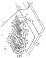
- Fig. 1 is a perspective view of essential portions of a display apparatus according to the present invention
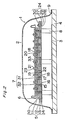
- Fig. 2 is a cross-sectional view of said display apparatus
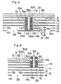
- Fig. 3 is a sectional view viewed in the direction of an arrow A of Fig. 1
- Fig. 4 is a sectional view viewed in the direction of an arrow B of Fig. 1
- Fig. 5 is a sectional view viewed in the direction of an arrow C of Fig. 1.
- a display apparatus 1 is comprised of a rear covering 2, a face plate 4 formed with a fluorescent screen 3, an electrode unit 5, line-shaped heat electrodes 6 as electron beam generating sources, and a rear electrode unit 7. On the predetermined position of the rear electrode unit 7 with line shaped heat electrodes 6 arranged on predetermined position thereof, the electrode unit 5 is fixed. This rear electrode unit 7 is positioned and fixed onto the face plate 4 with a plurality of posts 8 fixed onto the outer side of the fluorescent screen 3.
- the periphery of the rear covering 2 is air-tightly fixed to the face plate 4 with low melting point soldering glass 9, etc., and after evacuation through an evacuation tube (not shown), said evacuation tube is sealed, thereby to obtain a display apparatus 1, in which external electrode terminals and a getter, etc. are not shown.
- the electrode unit 5 is constituted by electron beam control electrodes 10, 11, 12, 13, and 14, a plurality of insulation spacers 15, 16, 17, 18, 19, 20, and 21, first pins 22 as the first coupling means for fixing the electrode unit 5, second pins 23 as the second coupling means for fixing the electrode unit 5 with the rear electrode unit 7, and a plurality of position restricting means 24 for restricting the positions of strip-shaped electrodes 13a, 13b, 13c to 13h which constitute the electron beam control electrode 13 and the positions of strip-shaped electrodes 14a, 14b, 14c to 14h which constitute the electron beam control electrode 14.
- the plate-shaped electron beam control electrodes 10, 11, and 12 have electron beam passing holes 10a, 11a, and 12a provided at respective predetermined positions thereof, and on the strip-shaped electrodes 13a, 13b, 13c to 13h which form the electron beam control electrode 13, comb-shaped projections 25 are formed on the predetermined positions thereof, and between respective strip-shaped electrodes 14a, 14b, 14c to 14h, slits 26 are formed on the predetermined position thereof in the longitudinal direction of line-shaped heat electrodes.
- the first metallic pins 22 for fixing the electrode unit 5 are fixed on the predetermined positions of strip-shaped electrodes 14a, 14b, 14c to 14h by welding or the like.
- Through holes 15a formed on the insulation spacers 15, through holes 13b formed on the electron beam control electrode 13, through holes 16a formed on the insulation spacers 16, through holes 12b formed on the electron beam control electrode 12, through holes 17a formed on the insulation spacers 17, through holes 11b formed on the electron beam control electrode 11, through holes 18a formed on the insulation spacers 18, and through holes 10b formed on the electron beam control electrode 10 are inserted into first pins 22, and through holes 19a formed on insulation spacers 19 are inserted into the first pins 22 projecting from the electron beam control electrode 10, and head portions of the first pins 22 are molten for example by the laser to fix electron beam control electrodes 10, 11, 12, 13 and 14.
- a plurality of position restricting means 24 are provided on both end portions in the longitudinal direction of the line-shaped heat electrodes 6.
- Position restricting holes 12c are provided on the plate-shaped electron beam control electrode 12 at its both end portions in the longitudinal direction of the line-shaped heat electrodes 6, and on strip-shaped electrodes 13a, 13b, 13c to 13h, and strip-shaped electrodes 14a, 14b, 14c to 14h, position restricting holes 13 i and 14 i substantially of the same diameter as 12c are formed at positions corresponding to position restricting holes 12c.
- one of the position restricting holes 13 i and 14 i may be long in the longitudinal direction of the hot cathodes 6.
- Bushings 27 are inserted into position restricting holes 12c, 13 i and 14 i , and metallic third pins 29 fixed on metallic fixing plates 28 by welding or the like are inserted into through holes 27a formed on bushings 27 from the sides of strip -shaped electrodes 14a, 14b, 14c to 14h, through holes 30a formed on insulation spacers 30 are inserted onto the third pins 29 projecting from the electron beam control electrodes 12, and the head portions of the third pins 29 are molten for example by laser, thereby to constitute the position restricting means 24.
- the rear electrode unit 7 is constituted by the rear electrode 31 and a support member 32 for supporting the hot cathodes 6, and the rear electrode 31 and the support member 32 are held at a predetermined spacing by an insulation layer 33.
- conductive films divided in a direction normal to the line-shaped hot cathodes 6 are formed on the side of the hot cathodes 6 via insulation films at the positions corresponding to the electron beam passing holes 10a, and by applying a predetermined voltage to said conductive films, electron beam is modulated.
- holes 32a are provided at the positions corresponding to the electron beam passing holes 10a. Furthermore, an insulation layer is formed on the hot cathode side of the support member 32.
- the second metallic pins 23 for fixing the electrode unit 5 and the rear electrode unit 7 are fixed at the predetermined positions of the plate-shaped electron beam control electrode 11 by welding, etc.
- the through holes 18a formed on the insulation spacers 18 and through holes 10c formed on the electron bean control electrode 10 are inserted into the second pins 23.
- through holes 20a formed on the insulation spacers 20 are inserted into second pins 23, and the rear electrode unit 7 with line-shaped hot cathodes 6 being arranged at the predetermined positions is disposed.
- through holes 21a of insulation spacers 21 are inserted, and the head portions of the second pins 23 are molten for example by laser , thereby to fix the electrode unit 5 and the rear electrode unit 7.
- the electrode unit 5 coupled to the rear electrode unit 7 is constructed. It is to be noted here that the insulation spacers 19 have a thickness equal to or smaller than those of the insulation spacers 20.
- the number of the electron beam control electrodes employed is not limited to the above.
- the electron beam control electrode for fixing the second pins 23 which couple the electrode unit 5 and the rear electrode unit 7 may be any electrode so long as it is not the electron beam control electrode 14 confronting the fluorescent screen.
- Said electron beams further pass through between the slits 28 of the electron beam control electrode 14 so as to be deflected in the normal direction to the line-shaped heat electrodes 6 through application of a voltage larger or smaller than the predetermined voltage to strip-shaped electrodes 14a, 14b, 14c to 14h.
- electron beams are focused, modulated, and deflected through passing through the electron beam control electrodes, and accelerated by the high voltage applied to the fluorescent screen 3 so as to collide with the fluorescent screen 3, thereby to emit fluorescent light for obtaining a picture.
- a plurality of electron beam control electrodes are fixed via insulation spacers at a predetermined interval without deformation thereof by first fixing pins so as to constitute the electrode unit, and by constructing said electrode unit at the room temperature without heating, the oxidization of the electrode unit is prevented, and by holding down each area of the insulation spacers within a smallest necessary area, each electrostatic capacitance between electron beam control electrodes can be fully decreased.
- the electrostatic capacitance can be reduced to 1/10 to 1/20 of that conventionally obtained.
- Fig. 6 is a perspective view of essential portions of a display apparatus according to the second embodiment of the present invention
- Fig. 7 is a cross-sectional view of said display apparatus
- Fig. 8 is a sectional view as viewed in the direction of arrow D in Fig. 6
- Fig. 9 is a sectional view as viewed in the direction of arrow E in Fig. 6
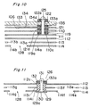
- Fig. 10 is a sectional view as viewed in the direction of arrow F in Fig. 6
- Fig. 11 is a sectional view as viewed in the direction of arrow G in Fig. 6.
- a display apparatus 101 is composed by a rear covering 102, a face plate 104 formed with a fluorescent screen 103 thereon, an electrode unit 105, line-shaped heat electrodes 106 as the electron beam generating sources, and a rear electrode unit 107.
- an electrode unit 105 is fixed on predetermined positions of a rear electrode unit 107 wherein the line-shaped heat electrodes 106 are arranged to be stretched in predetermined positions thereof.
- This rear electrode unit 107 is positioned with respect to the face plate 104 and fixed with set screws onto posts 108 which are fixed on the outer side of a fluorescent screen 103.
- the rear covering is air-tightly fixed to the face plate 104 with a low melting temperature soldering glass 109, or the like, after evacuation through an evacuation tube (not shown), the evacuation tube is sealed thereby to obtain a display apparatus 101.
- an evacuation tube not shown
- external electrode terminals , a getter,etc are not illustrated.
- the electrode unit 105 is composed by electron beam control electrodes 110, 111, 112, 113, and 114, a plurality of insulation spacers 115, 116, 117, 118, 119, 120, 121, and 122, first pins 123 and 124 which are coupling means for fixing the electrode unit 105, third pins 125 which are coupling means for fixing the electrode unit 105 with the rear electrode unit 107, and position restricting means for restricting positions of strip-shaped electrodes 113a, 113b, 113c to 113h constituting an electron beam control electrode 113 and strip-shaped electrodes 114a, 114b, 114c to 114h constituting an electron beam control electrode 114.
- plate-shaped electron beam control electrodes 110, 111, and 112 respectively have electron beam passing holes 110a, 111a and 112a on respective predetermined positions, while strip-shaped electrodes 113a, 113b, 113c to 113h constituting an electron beam control electrode 113 respectively have comb-shaped projections 127 on predetermined positions thereof and strip-shaped electrodes 114a, 114b, 114c to 114h constituting an electron beam control electrode 114 respectively have slits 128 formed therebetween at predetermined positions thereof in the longitudinal direction of the line-shaped heat electrodes 106.
- the metallic first pins 123 for fixing the first stage of the electrode unit 105 is fixed to the strip-shaped electrodes 114a, 114b, 114c to 114h at the predetermined position thereof by welding ,etc.
- through holes 115a formed on insulation spacers 115, through holes 113bb formed on the electron beam control electrodes 113, through holes 116a formed on insulation spacers 116, and through holes 112b formed on the electron beam control electrode 112 are inserted, and through holes 117a formed on insulation spacers 117 are inserted on the first pins 123 projecting from the electron beam control electrode 112, and the head portions of pins 123 are molten by laser,etc., thereby to fix electron beam control electrodes 112, 113, and 114.
- the second metallic pins 124 for fixing the second stage of the electrode unit 105 are fixed to the electron beam control electrode 112 at the predetermined positions thereof by welding ,etc.
- the second pins 124 through holes 118a formed on insulation spacers 118, through holes 111b formed on an electron beam control electrode 111, through holes 119a formed on insulation spacers 119 and through holes 110b formed on an electron beam control electrode 110 are inserted, and through holes 120a formed on insulation spacers 120 are inserted second pins 124 projecting from the electron beam control electrode 110, and by melting the head portions of said second pins 124 with laser, etc., electron beam control electrodes 110, 111, 112, 113, and 114 are fixed together.
- escape holes 111c for the head portions of pins 123.
- the electrode unit 105 is fixed in two divided stages by means of the first pins 123 and the second pins 124.
- strip-shaped electrodes 113a, 113b, 113c to 113h constituting the electron beam control electrode 113 and strip-shaped electrodes 114a, 114b, 114c to 114h constituting the electron beam control electrode 114 are independent respectively, a plurality of position restricting means 126 are arranged in the longitudinal directions of the line-shaped heat electrodes 106.
- position restricting holes 112c are formed, and on strip-shaped electrodes 113a, 113b, 113c to 113h and strip-shaped electrodes 114a, 114b, 114c to 114h, position restricting holes 113 i and 114 i of substantially the same diameter as that of the hole 112c are formed at positions corresponding to 112c.
- one of position restricting holes 113 i and 114 i may be long holes in the longitudinal directions of the line-shaped heat electrodes 106.
- Position restricting bushings 129 are inserted into position restricting holes 112c, 113 i and 114 i , and fourth metallic pins 131 fixed to metallic fixing plates 130 by welding ,etc. are inserted into through holes 129a formed in the bushings 129 from the sides of the strip-shaped electrodes 114a, 114b, 114c to 114h, and through holes 132a formed on insulation spacers 132 are inserted into fourth pins 131 projecting from the electron beam control electrode 112, and the head portions of the fourth pins 131 are molten , thereby to constitute position restricting means 126.
- a rear electrode unit 107 is composed of a rear electrode 133 and a support member 134 for supporting the line-shaped heat electrodes 106, and the rear electrode 133 and the support member 134 are maintained at a predetermined interval by an insulation layer 135.
- conductive films divided in the direction normal to the line-shaped electrodes 106 are formed at positions corresponding to electron beam passing holes 110a via insulation layer on the side of linear hot cathodes 106, and by applying a predetermined voltage to said conductive films, electron beams are modulated.
- On the support member 134 there are provided holes 134a at positions corresponding to electron beam passing holes 110a.
- an insulation layer on the linear hot chatodes 106 side By contacting the linear hot cathodes 106 with bars between respective holes 134a of support member 134, the vibration of the line-shaped heat electrodes 106 are prevented.
- third metallic pins 125 for fixing the electrode unit 105 with the rear electrode unit 107 are fixed to the plate-shaped electron beam control electrode 111 at its predetermined positions.
- third pins 125 In fixing the electrode unit 105, though holes 119a formed on insulation spacers 119 and through holes 110c formed on the electron beam control electrode 110 are inserted into third pins 125. Furthermore, through holes 121a formed on insulation spacers 121 are inserted into third pins 125, and the rear electrode unit 107 with the line-shaped heat electrodes 106 being stretchedly arranged at its predetermined positions is arranged.
- escape holes 134c for the head portions of second pins 124 for fixing the electrode unit 105, through holes 134d for third pins 125, while on the rear electrode 133, there are formed through holes 133a for third pins 125.
- the electrode unit 105 coupled to the rear electrode unit 107 is constructed.
- each insulation spacer 117 has a thickness equal to or smaller than that of the insulation spacer 118
- each insulation spacer 120 has a thickness equal to or smaller than that of the insulation spacer 121.
- the number of electrodes is not limited to five
- the electron beam control electrodes fixed by the first pins 123 are not limited to the above-mentioned electrodes 112, 113, and 114.
- the electron beam control electrode for fixing the second pins 124 may be any electron beam control electrode fixed by the first pins 123 so long as it is not the electron beam control electrode 114 confronting the fluorescent screen 103.
- the electron beam control electrode for fixing the third pins 125 for coupling the electrode unit 105 and the rear electrode unit 107 may be any electron beam control electrode excluding the electron beam control electrode 114 confronting the fluorescent screen 103.
- the electrode unit 105 may be divided into more than three stages in the lamination direction for fixing.
- the electrode unit is fixed in two stages by first and second pins without deforming a plurality of electron beam control electrodes and maintaining a predetermined spacing between respective electrodes, and said electrode unit is constructed at the room temperature without heating, the oxidization thereof can be prevented, and furthermore, by holding down the areas of respective insulation spacers to the smallest areas necessary for fixing, the electrostatic capacitances between respective electrodes can be fully decreased.
- the electrostatic capacitance can be made 1/10 to 1/20 of the value obtained conventionally.
- the electrode unit is divided in the lamination direction for fixing with the first and second pins, and fixing with the first pins is effected with an electron beam control electrode except for the electron beam control electrode confronting the fluorescent screen, the deformations of the electron beam control electrodes arising from the temperature rise difference therebetween accompanying the heating of the line-shaped heat electrodes can be prevented from affecting strip-shaped electrodes constituting the electron beam control electrode confronting the fluorescent screen.
- the fixing of the electrode unit with the rear electrode unit is effected by the third pins fixed onto an electron beam control electrode excluding that confronting the fluorescent screen, the strains arising from the fixing of the rear electrode unit and the electrode unit can be prevented from reaching the electron beam control electrode confronting the fluorescent screen.
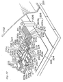
- Fig. 12 is a perspective view of essential portions of a display apparatus according to the present embodiment
- Fig. 13 is a cross-sectional view of said display apparatus
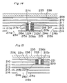
- Fig. 14 is a sectional view as viewed in the direction of arrow H in Fig. 12
- Fig. 15 is a sectional view as viewed in the direction of arrow I in Fig. 12.
- Fig. 16 is a sectional view as viewed in the direction of arrow J in Fig. 12
- Fig. 17 is a sectional view as viewed in the direction of arrow K in Fig . 12
- Fig. 18 is a sectional view as viewed in the direction of arrow L on Fig. 2.
- a display apparatus 201 is composed by a rear covering 202, a face plate 204 formed with a fluorescent screen 203, an electrode unit 205, line-shaped heat electrodes 206, and a rear electrode unit 207,
- the electrode unit 205 is fixed on the rear electrode unit 207 at its predetermined positions, with line-shaped heat electrodes 206 being arranged stretched at its predetermined positions.
- This rear electrode unit 207 is positioned and fixed onto the face plate 204 at a plurality of posts 208 fixed to the outer side of the florescent screen 207 with set screws.
- the rear covering 202 is air-tightly fixed to the face plate 204 with a low melting point soldering glass 209, etc, and after evacuation through an evacuation tube (not shown), said evacuation tube is sealed, thereby to obtain said display apparatus 201.
- an evacuation tube not shown
- external electrode terminals, a getter, etc are not shown.
- the electrode unit 205 is composed of electron beam control electrodes 210, 211, 212, 213, and 214, a plurality of insulation spacers 215, 216, 217, 218, 219, 220, 221, 222, and 223, first, second and third pins 224, 225, and 226 as coupling means for fixing the electrode unit 205, fourth pins 227 as the coupling means 228 for fixing the electrode unit 205 with the rear electrode unit 207, and a plurality of position restricting means for restricting positions of strip-shaped electrodes 213a, 213b, 213c to 213h constituting the electron beam control electrode 213, and strip-shaped electrodes 214a, 214b, 214c to 214h constituting the electron beam control electrode 214.
- Plate-shaped electron beam control electrodes 210, 211, and 212 respectively have electron beam passing holes 210a, 211a, and 212a at predetermined positions thereof, while strip-shaped electrodes 213a, 213b, 213c to 213h constituting the electron beam control electrode 213 have comb-shaped projections 229 at respective predetermined positions and strip-shaped electrodes 214a, 214b, 214c to 214h constituting the electron beam control electrode 214 have slits 230 formed therebetween at predetermined positions in the longitudinal directions of the line-shaped heat electrode 206.
- the electrode unit 205 is divided into a first electrode unit 205a composed of electron beam control electrodes 212, 213 and 214 and a second electrode unit 205b composed of electron beam control electrodes 210 and 211.
- First metallic pins 224 for fixing the first electrode unit 205a are fixed on strip-shaped electrodes 214a, 214b, 214c to 214h of the electron beam control electrode 214 at predetermined positions thereof with welding, etc.
- Through holes 215a formed on insulation spacers 215, through holes 212b formed on the electron beam control electrode 212, through holes 216a formed on insulation spacers 216 and through holes 213bb formed on the electron beam control electrode 213 are inserted onto the first pins 224, and through holes 217a formed on insulation spacers 217 are inserted onto the first pins 224 projecting from the electron beam control electrode 212, and the head portions of the first pins 224 are molten for example, with laser, thereby to fix the first electrode unit 205a.
- Second metallic pins 225 for fixing the second electrode unit 205b are fixed on the electron beam control electrode 211 at its predetermined positions by welding ,etc.
- Through holes 220a formed on insulation spacers 220, and through holes 210b formed on the electron bean control electrode 210 are inserted onto second pins 225, through holes 221a formed on insulation spacers 221 are inserted onto the second pins 225 projecting from the electron beam control electrode 210, and the head portions of said second pins 225 are molten, for example, by laser,thereby to fix the second electrode unit 205b.
- first electrode unit 205a and the second electrode unit 205b are fixed by third pins 226 being fixed to the electron beam control electrode 212 at its predetermined positions by welding, etc.
- Third pins 226 are inserted into through holes 218a formed on insulation spacers 218 and through holes 211b formed on the electron beam control electrode 211, and though holes 219a formed on insulation spacers 219 are inserted onto the second pins 226 projection from the electron beam control electrode 211, and the head portions of said third pins 226 are molten, for example, by laser, thereby to coupe and fix the first electrode unit 205a and the second electrode unit 205b.
- escape holes 211c for the head portions of first pins 224 are formed on the electron beam control electrode 211, and through holes 210c for the fixing portions of third pins 226 are formed on the electron beam control electrode 210.
- the electrode unit 205 is divided into two units,i.e. the first electrode unit 205a and the second electrode unit 205b to be fixed respectively by means of first pins 224 and second pins 225, and said first electrode unit 205a and second electrode unit 205b are fixed together by means of third pins 226, thereby to constitute the electrode unit 205.
- strip-shaped electrodes 213a, 213b, 213c to 213h constituting the electron beam control electrode 213 and strip-shaped electrodes 214a, 214b, 214c to 214h constituting the electron beam control electrode 214 are respectively independent, a plurality of position restricting means 228 are provided on both end portions thereof in the longitudinal directions of said line-shaped electrodes 206.
- each position restricting hole 213 i and each position restricting hole 214 i may be of a hole long in the longitudinal direction of the line-shaped heat electrode 206.
- Position restricting bushings 231 are inserted into position restricting holes 212c, 213 i and 214 i , metallic fifth pins 233 fixed at the fixing plate 232 by welding ,etc. are inserted into though holes 231a formed on bushings 231 from the sides of strip-shaped electrodes 214a, 214b, 214c to 214h, through holes 234a formed on insulation spacer 234 are inserted onto the fifth pins 233 projecting from the electron beam control electrode 212, and the head portions of the fifth pins 233 are molten ,for example, by laser, thereby to constitute position restricting means 228.
- the rear electrode unit 207 is composed by a rear electrode 235 and a support member 236 for supporting linear hot cathodes 206, with a predetermined spacing being maintained therebetween by an insulation layer 237.
- the rear electrode 235 is formed, on its side of linear hot cathodes 206 via insulation layers, with conductive films divided in the direction normal to linear hot cathodes 206 at positions corresponding to electron beam passing holes 210a, and by applying a predetermined voltage to these conductive films, electron beams are modulated.
- the support member 236 are formed with holes 236a at positions corresponding to electron beam passing holes 210a, and also formed with an insulation layer on its linear hot cathode 206 side.
- the fourth metallic pins 227 for fixing the electrode unit 205 and the rear electrode unit 207 are fixed at predetermined positions of the electron beam control electrode 211 by welding ,etc.
- the fourth pins 227 are inserted into through holes 220a formed on insulation spacers 220, and through holes 210a formed on the electron beam control electrode 210, and further inserted into through holes 222a formed on insulation spacers 222, and the rear electrode unit 207 with linear hot cathodes 206 stretchedly arranged at its predetermined positions is arranged.
- escape holes 236c for the head portions of second pins 225 for fixing the electrode unit 205 and escape holes 236d for fourth pins 227, while on the rear electrode 235, there are formed through holes 235a for fourth pins 227.
- Through holes 223a of insulation spacers 223 are inserted onto the fourth pins 227 projecting from the rear electrode unit 207, and the head portions of said pins 227 are molten , for example, by laser, thereby to fix the electrode unit 205 with the rear electrode unit 207.
- the assembly of the electrode unit 205 and the rear electrode unit 207 is constituted.
- each insulation spacer 217 has a thickness equal to or smaller than that of insulation spacer 218, each insulation spacer 219 has a thickness equal to or smaller than that of insulation spacer 220, and each insulation spacer 221 has a thickness equal to or smaller than that of insulation spacer 222.
- the number of the electron beam control electrodes is not limited to five pieces
- the first electrode unit 205a fixed by the first pins 224 is not limited to electron beam control electrodes 212, 213 and 214
- the second electrode unit 205b fixed by the second pins 226 is not limited to the electron beam control electrodes 210 and 211.
- the electron beam control electrode for fixing the third pins 226 for coupling and fixing the first electrode unit 205a and the second electrode unit 205b may any electron beam control electrode fixed by the first pins 224 excluding that confronting the fluorescent screen 203.
- the electron beam control electrode for fixing the fourth pins 227 for coupling and fixing the electrode unit 05 and the rear electrode unit 207 may be any electron beam control electrode excluding the electron beam control electrode 214 confronting the fluorescent screen 203. Furthermore, the electrode unit may be divided into more than three stages in the lamination direction, thus to be fixed.
- the electrostatic capacitances between respective electron beam control electrodes can be fully decreased.
- the electrostatic capacitances can be made 1/10 to 1/20 of the value obtained conventionally.
- the electrode unit is divided in two stages in the lamination direction for fixing with first and second pins, and the fixing with the first pins is effected with an electron beam control electrode excluding the electron beam control electrode confronting linear hot cathodes, the deformations of electron beam control electrodes arising from the temperature rise differences therebetween accompanying the heating of linear hot cathodes can be prevented from affecting strip-shaped heat electrodes constituting the electron beam control electrode confronting the fluorescent screen.
- the fixing of the electrode unit and the ear electrode unit is effected by the fourth pins fixed on an electron beam control electrode excluding the electron beam control electrode confronting the fluorescent screen, the strains arising from the fixing of the electrode unit and the rear electrode unit can be prevented from affecting the strip-shaped electrodes constituting the electron beam control electrode confronting the fluorescent screen.
- a plurality of electron beam control electrodes are fixed through insulation spacers with pin without deformation thereof and maintaining a predetermined spacing therebetween, and by constructing the electrode unit at the room temperature without heating, the oxidization of the electrode unit can be prevented, and furthermore, by holding down the areas of insulation spacers to the smallest areas necessary to fix electrodes, the electrostatic capacitances can be fully decreased.
- the fixing of the rear electrode unit and the electrode unit is effected by pins fixed on an electron beam control electrode excluding the electron beam control electrode confronting the florescent screen, the strain arising from the fixing of the rear electrode unit and the electrode unit can be prevented from affecting the strip-shaped electrodes.
- the electrode unit is fixed through dividing in the lamination direction, and the fixing by the pins fixed on the electron beam control electrode confronting the fluorescent screen is effected with an electron beam control electrode excluding the electron beam control electrode confronting linear hot cathodes, the deformation of respective electron beam control electrodes due to the temperature rise differences therebetween accompanying the heating of line-shaped heat electrodes can be prevented from affecting the strip-shaped electrodes confronting the fluorescent screen.
Landscapes
- Cathode-Ray Tubes And Fluorescent Screens For Display (AREA)
Applications Claiming Priority (2)
| Application Number | Priority Date | Filing Date | Title |
|---|---|---|---|
| JP297962/90 | 1990-11-01 | ||
| JP2297962A JPH04169047A (ja) | 1990-11-01 | 1990-11-01 | 表示装置 |
Publications (1)
| Publication Number | Publication Date |
|---|---|
| EP0487936A1 true EP0487936A1 (de) | 1992-06-03 |
Family
ID=17853345
Family Applications (1)
| Application Number | Title | Priority Date | Filing Date |
|---|---|---|---|
| EP91118716A Withdrawn EP0487936A1 (de) | 1990-11-01 | 1991-11-04 | Anzeigegerät |
Country Status (4)
| Country | Link |
|---|---|
| US (1) | US5247225A (de) |
| EP (1) | EP0487936A1 (de) |
| JP (1) | JPH04169047A (de) |
| KR (1) | KR920010730A (de) |
Cited By (2)
| Publication number | Priority date | Publication date | Assignee | Title |
|---|---|---|---|---|
| EP0573027A1 (de) * | 1992-06-04 | 1993-12-08 | Matsushita Electric Industrial Co., Ltd. | Bildanzeigevorrichtung und Herstellungsverfahren |
| EP0631296A1 (de) * | 1993-05-26 | 1994-12-28 | Matsushita Electric Industrial Co., Ltd. | Apparatus für Flachbildwiedergabe |
Families Citing this family (9)
| Publication number | Priority date | Publication date | Assignee | Title |
|---|---|---|---|---|
| JPH04255651A (ja) * | 1991-02-08 | 1992-09-10 | Matsushita Electric Ind Co Ltd | 平板型表示装置およびその駆動方法 |
| JP3189531B2 (ja) * | 1993-10-01 | 2001-07-16 | 松下電器産業株式会社 | 平板電極ユニットおよびその製造方法 |
| US5610208A (en) | 1994-02-17 | 1997-03-11 | Nippon Shokubai Co., Ltd. | Water-absorbent agent, method for production thereof, and water-absorbent composition |
| KR100470338B1 (ko) * | 2002-06-07 | 2005-02-05 | 엘지.필립스 디스플레이 주식회사 | 평판 디스플레이 장치 및 그 제조 방법 |
| US6984991B2 (en) * | 2004-05-11 | 2006-01-10 | International Business Machines Corporation | Initialization of a bidirectional, self-timed parallel interface with automatic testing of AC differential wire pairs |
| JP4216764B2 (ja) * | 2004-05-21 | 2009-01-28 | 株式会社日立製作所 | ディスプレイ装置並びにディスプレイモジュール及びディスプレイパネル |
| WO2008009898A1 (en) * | 2006-07-20 | 2008-01-24 | Aviza Technology Limited | Ion sources |
| JP2009112094A (ja) * | 2007-10-29 | 2009-05-21 | Toyota Industries Corp | 回転電機における相間絶縁シート及び電動圧縮機 |
| US20130015757A1 (en) * | 2011-07-11 | 2013-01-17 | Hariharakeshava Sarpangala Hegde | Multi-grid assembly in plasma source system and methods for improving same |
Citations (1)
| Publication number | Priority date | Publication date | Assignee | Title |
|---|---|---|---|---|
| EP0316871A2 (de) * | 1987-11-16 | 1989-05-24 | Matsushita Electric Industrial Co., Ltd. | Bildwiedergabevorrichtung |
Family Cites Families (7)
| Publication number | Priority date | Publication date | Assignee | Title |
|---|---|---|---|---|
| EP0025221B1 (de) * | 1979-09-05 | 1983-06-29 | Kabushiki Kaisha Toshiba | Flache Anzeigevorrichtung |
| JPS59148252A (ja) * | 1983-02-14 | 1984-08-24 | Matsushita Electric Ind Co Ltd | 平板型表示装置 |
| JPS60218750A (ja) * | 1984-04-13 | 1985-11-01 | Matsushita Electric Ind Co Ltd | 平面型表示装置 |
| JPS6337936A (ja) * | 1986-07-31 | 1988-02-18 | 出光石油化学株式会社 | 樹脂積層体 |
| US4887000A (en) * | 1986-11-06 | 1989-12-12 | Sushita Electric Industrial Co., Ltd. | Electron beam generation apparatus |
| NL8700487A (nl) * | 1987-02-27 | 1988-09-16 | Philips Nv | Vacuuembuis met elektronenoptiek. |
| JPH02213034A (ja) * | 1989-02-14 | 1990-08-24 | Matsushita Electric Ind Co Ltd | 平板型表示装置 |
-
1990
- 1990-11-01 JP JP2297962A patent/JPH04169047A/ja active Pending
-
1991
- 1991-10-31 US US07/785,751 patent/US5247225A/en not_active Expired - Fee Related
- 1991-11-01 KR KR1019910019421A patent/KR920010730A/ko not_active Abandoned
- 1991-11-04 EP EP91118716A patent/EP0487936A1/de not_active Withdrawn
Patent Citations (1)
| Publication number | Priority date | Publication date | Assignee | Title |
|---|---|---|---|---|
| EP0316871A2 (de) * | 1987-11-16 | 1989-05-24 | Matsushita Electric Industrial Co., Ltd. | Bildwiedergabevorrichtung |
Non-Patent Citations (2)
| Title |
|---|
| PATENT ABSTRACTS OF JAPAN vol. 10, no. 69 (E-389)(2126) 18 March 1986 & JP-A-60 218 750 ( MATSUSHITA ) 1 November 1985 * |
| PATENT ABSTRACTS OF JAPAN vol. 8, no. 281 (E-286)(1718) 21 December 1984 & JP-A-59 148 252 ( MATSUSHITA ) 24 August 1984 * |
Cited By (3)
| Publication number | Priority date | Publication date | Assignee | Title |
|---|---|---|---|---|
| EP0573027A1 (de) * | 1992-06-04 | 1993-12-08 | Matsushita Electric Industrial Co., Ltd. | Bildanzeigevorrichtung und Herstellungsverfahren |
| EP0631296A1 (de) * | 1993-05-26 | 1994-12-28 | Matsushita Electric Industrial Co., Ltd. | Apparatus für Flachbildwiedergabe |
| US5461396A (en) * | 1993-05-26 | 1995-10-24 | Matsushita Electric Industrial Co., Ltd. | Flat-type picture display apparatus |
Also Published As
| Publication number | Publication date |
|---|---|
| JPH04169047A (ja) | 1992-06-17 |
| KR920010730A (ko) | 1992-06-27 |
| US5247225A (en) | 1993-09-21 |
Similar Documents
| Publication | Publication Date | Title |
|---|---|---|
| EP0487936A1 (de) | Anzeigegerät | |
| EP0404022B1 (de) | Flache Bildwiedergabevorrichtung und Verfahren zur Herstellung derselben | |
| US4955681A (en) | Image display apparatus having sheet like vertical and horizontal deflection electrodes | |
| JPH0246646A (ja) | 電子管 | |
| JPH08293270A (ja) | 平板型表示装置 | |
| JP3060766B2 (ja) | 画像表示装置とその製造方法 | |
| KR100638906B1 (ko) | 칼라 평면 디스플레이 소자 | |
| JP2911161B2 (ja) | フラットディスプレイ装置 | |
| US6900585B2 (en) | Spacer for an electrode of a color flat panel display | |
| JPS59148252A (ja) | 平板型表示装置 | |
| JPH04160724A (ja) | 電極ユニットの製造方法 | |
| JPS6334842A (ja) | 画像表示装置 | |
| CN1174397A (zh) | 阴极构件和采用这种构件的阴极射线管的电子枪 | |
| JP2966585B2 (ja) | フラットディスプレイの端子部補強構造 | |
| JPS62143347A (ja) | 画像表示装置 | |
| JPH11185672A (ja) | 平板型表示装置 | |
| US20030173888A1 (en) | Flat panel display | |
| JPH05144390A (ja) | 表示装置 | |
| JPH087801A (ja) | 受像管用板状電極の支持方法 | |
| KR20030028064A (ko) | 평판형 화상표시장치 및 그 제조방법 | |
| JPH08335444A (ja) | 平板型画像表示装置 | |
| JPS62154437A (ja) | 画像表示装置 | |
| JPH04341733A (ja) | 電極ユニット | |
| JP2007073236A (ja) | 画像表示装置 | |
| JP2005310648A (ja) | メッシュ構造の四極電界放射ディスプレイおよびその製造方法 |
Legal Events
| Date | Code | Title | Description |
|---|---|---|---|
| PUAI | Public reference made under article 153(3) epc to a published international application that has entered the european phase |
Free format text: ORIGINAL CODE: 0009012 |
|
| 17P | Request for examination filed |
Effective date: 19911104 |
|
| AK | Designated contracting states |
Kind code of ref document: A1 Designated state(s): DE FR GB |
|
| 17Q | First examination report despatched |
Effective date: 19950117 |
|
| STAA | Information on the status of an ep patent application or granted ep patent |
Free format text: STATUS: THE APPLICATION HAS BEEN WITHDRAWN |
|
| 18W | Application withdrawn |
Withdrawal date: 19950408 |