EP0488111B1 - Système de disque optique - Google Patents
Système de disque optique Download PDFInfo
- Publication number
- EP0488111B1 EP0488111B1 EP91120064A EP91120064A EP0488111B1 EP 0488111 B1 EP0488111 B1 EP 0488111B1 EP 91120064 A EP91120064 A EP 91120064A EP 91120064 A EP91120064 A EP 91120064A EP 0488111 B1 EP0488111 B1 EP 0488111B1
- Authority
- EP
- European Patent Office
- Prior art keywords
- signal
- digital
- analog
- converter
- audio signal
- Prior art date
- Legal status (The legal status is an assumption and is not a legal conclusion. Google has not performed a legal analysis and makes no representation as to the accuracy of the status listed.)
- Expired - Lifetime
Links
Images

Classifications
-
- H—ELECTRICITY
- H04—ELECTRIC COMMUNICATION TECHNIQUE
- H04N—PICTORIAL COMMUNICATION, e.g. TELEVISION
- H04N9/00—Details of colour television systems
- H04N9/79—Processing of colour television signals in connection with recording
- H04N9/80—Transformation of the television signal for recording, e.g. modulation, frequency changing; Inverse transformation for playback
- H04N9/82—Transformation of the television signal for recording, e.g. modulation, frequency changing; Inverse transformation for playback the individual colour picture signal components being recorded simultaneously only
- H04N9/8205—Transformation of the television signal for recording, e.g. modulation, frequency changing; Inverse transformation for playback the individual colour picture signal components being recorded simultaneously only involving the multiplexing of an additional signal and the colour video signal
- H04N9/8211—Transformation of the television signal for recording, e.g. modulation, frequency changing; Inverse transformation for playback the individual colour picture signal components being recorded simultaneously only involving the multiplexing of an additional signal and the colour video signal the additional signal being a sound signal
- H04N9/8216—Transformation of the television signal for recording, e.g. modulation, frequency changing; Inverse transformation for playback the individual colour picture signal components being recorded simultaneously only involving the multiplexing of an additional signal and the colour video signal the additional signal being a sound signal using time division multiplex
-
- H—ELECTRICITY
- H04—ELECTRIC COMMUNICATION TECHNIQUE
- H04N—PICTORIAL COMMUNICATION, e.g. TELEVISION
- H04N9/00—Details of colour television systems
- H04N9/79—Processing of colour television signals in connection with recording
- H04N9/7904—Processing of colour television signals in connection with recording using intermediate digital signal processing
Definitions
- This invention relates to an optical disk information recording system of the kind as defined in the preamble of claim 1 and to an optical-disk information reproducing system.
- An optical disk is a recording medium which can store a large amount of information.
- An optical-disk information recording system of the above-referenced kind is disclosed in the post-published US-A-5 063 447 claiming the priority of the prepublished JP-A-2057079.
- an A/D converter is used for an analog-to-digital conversion of an analog video signal from an image signal processing circuit and of an analog audio signal from a voice processing circuit.
- the digital video signal is stored in field memories in a frame memory.
- the digital audio signal is stored in a voice signal memory.
- the frequency of clocks supplied to the A/D converter is lower than that of the clocks at the time of converting the analog video signal.
- the frequency of clocks supplied to the A/D converter is changed depending on whether an image signal or an audio signal is handled.
- a D/A converter is provided for converting the stored digital video signal and the stored digital audio signal received via a switch for selecting the one or the other of these stored signals.
- the analog signals from the D/A converter are fed to a record signal processing circuit before being FM modulated.
- the frequency of the sampling clocks which are supplied to the D/A converter is set to a speed which can be similar or higher than in the case of the image signal.
- an analog video signal is recorded on and reproduced from a recording medium by frequency modulation and demodulation.
- a circuit is provided for digitally separating the video signal to a first frequency band signal and a second frequency band signal including a color subcarrier.
- Another circuit converts the frequency band signal to first and second base band signals.
- a circuit for time-compressing at least the first and second base band signals a circuit for recording and reproducing the first frequency band signal and the time-compressed first and second base band signal in an analog mode, a circuit for digitally recombining the reproduced first frequency band signal and the time-compressed first and second base band signals, and a circuit for converting the recombined digital video signal to the analog composite color video signal.
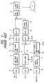
- Fig. 1 is a block diagram of a prior art recording system.
- Fig. 2 is a block diagram of a prior art reproducing system.
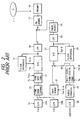
- Fig. 3 is a block diagram of a recording system according to an embodiment of this invention.
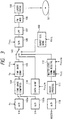
- Fig. 4 is a block diagram of a reproducing system according to an embodiment of this invention.
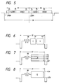
- Fig. 5 is a time domain diagram showing the contents of a signal recorded on the optical disk of Fig. 3.
- Fig. 6 is a time domain diagram showing the contents of a baseband video signal inputted into the FM modulation circuit of Fig. 3.
- Fig. 7 is a time domain diagram showing the contents of a baseband audio signal inputted into the FM modulation circuit of Fig. 3.
- Fig. 8 is a time domain diagram showing the contents of a baseband data signal inputted into the FM modulation circuit of Fig. 3.
- a prior art system for recording information on an optical disk 1 includes analog-to-digital (A/D) converters 3a and 3b receiving component analog video signals, that is, an analog luminance signal Y and an analog color signal C respectively.
- the analog luminance signal Y and the analog color signal C are converted by the A/D converters 3a and 3b into corresponding digital signals respectively.
- the A/D conversion of the analog luminance signal Y and the analog color signal C uses a sampling clock signal having a predetermined frequency "fs".
- the digital luminance signal and the digital color signal outputted from the A/D converters 3a and 3b are subjected to a time base compression process or a time base adjustment process, and are multiplexed or combined into a composite video signal by a time base compression circuit 4.
- the composite video signal outputted from the time base compression circuit 4 is subjected to a time base conversion process by a time base conversion circuit 5.
- the time base conversion process uses the clock signal of the frequency "fs" and a second clock signal of a predetermined frequency "ftci”.
- the digital video signal outputted from the time base conversion circuit 5 has a clock period corresponding to the time base conversion frequency "ftci”.
- the digital video signal outputted from the time base conversion circuit 5 is converted by a digital-to-analog (D/A) converter 6 into a corresponding analog signal.
- the D/A conversion of the digital video signal uses the clock signal of the frequency "ftci”.
- the analog video signal outputted from the D/A converter 6 is transmitted to an FM modulation circuit (a frequency-modulation circuit) 8 via a low pass filter 7 and a switch (no reference numeral).
- the analog video signal is multiplexed with an analog audio signal by the switch before entering the FM modulation circuit 8.
- the FM modulation circuit 8 modulates the frequency of a carrier in accordance with the received analog video signal, and converts the analog video signal into an FM video signal.
- a laser drive circuit 9 drives a laser light source (not shown) in response to the output FM video signal from the FM modulation circuit 8 so that a laser light beam emitted from the laser light source will be modulated in accordance with the FM video signal.
- the laser light beam is applied to the optical disk 1 so that information represented by the FM video signal will be recorded on the optical disk 1.
- An analog audio signal (an analog audio-information signal) is converted by an A/D converter 10 into a corresponding digital signal.
- the digital audio signal outputted from the A/D converter 10 is processed by an audio signal processor 11.
- the audio signal processor 11 executes an error correction code adding process and an interleaving process on the digital audio signal.
- the audio signal processor 11 outputs a binary digital audio signal having a predetermined data rate "fa".
- the digital audio signal outputted from the audio signal processor 11 is converted by a digital signal conversion circuit 12 into a multi-level form digital signal which has ''2 l ''' discrete amplitude levels and which has a predetermined data rate "fa/l", where the character ''2 l ''' denotes the total number of the discrete amplitude levels and the character "l” denotes a predetermined integer.
- This signal conversion uses a clock signal having a frequency "fa” and a clock signal having a frequency "fa/l”.
- the multi-level form digital audio signal outputted from the digital signal conversion circuit 12 is transmitted to a D/A converter 13 via a switch (no reference numeral).
- the multi-level form digital audio signal outputted from the digital signal conversion circuit 12 is converted by the D/A converter 13 into a corresponding analog signal.
- the D/A conversion of the multi-level form digital audio signal uses the clock signal of the frequency "fa/l".
- the analog audio signal outputted from the D/A converter 13 is transmitted to the FM modulation circuit 8 via a low pass filter 14, a phase adjustment circuit 15, and the switch (no reference numeral).
- the analog audio signal is multiplexed with the analog video signal by the switch before entering the FM modulation circuit 8.
- the FM modulation circuit 8 modulates the frequency of a carrier in accordance with the received analog audio signal, and converts the analog audio signal into an FM audio signal.
- the laser drive circuit 9 drives the laser light source (not shown) in response to the output FM audio signal from the FM modulation circuit 8 so that the laser light beam emitted from the laser light source will be modulated in accordance with the FM audio signal.
- the laser light beam is applied to the optical disk 1 so that information represented by the FM audio signal will be recorded on the optical disk 1.
- the low pass filter 7 for processing the video signal and the low pass filter 14 for processing the audio signal have different pass bands, so that the low pass filters 7 and 14 provide different group delay times.
- the phase adjustment circuit 15 serves to compensate for the difference between the group delay times provided by the low pass filters 7 and 14.
- a data signal generation circuit 16 outputs a digital data signal at a predetermined data rate "fa/l/k", where the character "k” denotes a predetermined integer.
- the output digital data signal from the data signal generating circuit 16 represents addresses and time codes denoting positions of the video signal and the audio signal on programs.
- the output digital data signal from the data signal generation circuit 16 is multiplexed with the output audio signal from the digital signal conversion circuit 12 by the switch (no reference character), and is then transmitted to the D/A converter 13.
- the prior art recording system of Fig. 1 has the following problems. Since the video time base conversion frequency "ftci" completely disagrees with the audio data rate "fa”, it is necessary to provide the two D/A converters 6 and 13, and the two low pass filters 7 and 14. In addition, it is necessary to provide the phase adjustment circuit 15. In the event that the clock signal having the frequency "ftci" leaks to the system portion operated in response to the clock signal having the frequency "fa” and that the clock signal having the frequency "fa” leaks to the system portion operated in response to the clock signal having the frequency "ftci", there occurs crosstalk between the independent signals in the two system portions.
- a prior art system for reproducing information from an optical disk 1 includes a preamplifier 16 and an FM demodulation circuit 17.
- An information signal reproduced from the optical disk 1 is transmitted to the FM demodulation circuit 17 via the preamplifier 16.
- the reproduced signal is subjected to an FM demodulation process by the FM demodulation circuit 17, being converted into a reproduced baseband analog signal.
- the reproduced analog signal outputted from the FM demodulation circuit 17 is demultiplexed by a switch (no reference character) into a reproduced analog video signal and a reproduced analog audio signal.
- the reproduced analog video signal is transmitted to a clock reproduction circuit 17 and an A/D converter 20 via a low pass filter 18.
- the reproduced analog audio signal is transmitted to a clock reproduction circuit 26 and an A/D converter 27 via a phase adjustment circuit 24 and a low pass filter 25.
- the low pass filter 18 for processing the video signal and the low pass filter 25 for processing the audio signal have different pass bands, so that the low pass filters 18 and 25 provide different group delay times.
- the phase adjustment circuit 24 serves to compensate for the difference between the group delay times provided by the low pass filters 18 and 25.
- the reproduced analog video signal is further processed as follows.
- the clock reproduction circuit 17 reproduces a clock signal from the reproduced analog video signal by using a PLL (phase-locked loop).
- the reproduced clock signal has the frequency "ftci”.
- the reproduced analog video signal is converted by the A/D converter 20 into a corresponding digital signal.
- the A/D conversion of the reproduced analog video signal uses the clock signal having the frequency "ftci”.
- the reproduced digital video signal outputted from the A/D converter 20 is subjected to a time base conversion process by a time base conversion circuit 21.
- the time base conversion process uses the clock signal of the frequency "ftci" and a second clock signal of the sampling frequency "fs".
- the reproduced digital video signal outputted from the time base conversion circuit 21 has a data rate corresponding to the sampling frequency "fs".
- the reproduced digital video signal outputted from the time base conversion circuit 21 is subjected to a time base expansion process or a time base adjustment process, and is demultiplexed into a reproduced digital luminance signal and a reproduced digital color signal by a time base expansion circuit 22.
- the reproduced digital luminance signal is converted by a D/A converter 23a into a corresponding reproduced analog luminance signal Y.
- the reproduced digital color signal is converted by a D/A converter 23b into a corresponding reproduced analog color signal C.
- the D/A conversion of the reproduced digital luminance signal and the reproduced digital color signal uses the sampling clock signal of the frequency "fs".
- the reproduced analog audio signal is further processed as follows.
- the clock reproduction circuit 26 reproduces a clock signal from the reproduced analog audio signal by using a PLL (phase-locked loop).
- the reproduced clock signal has the frequency "fa/l”.
- the reproduced analog audio signal is converted by the A/D converter 27 into a corresponding digital signal.
- the A/D conversion of the reproduced analog audio signal uses the clock signal having the frequency "fa/l”.
- the reproduced digital audio signal outputted from the A/D converter 27 is demultiplexed by a switch (no reference numeral) into a reproduced digital pure audio signal and a reproduced digital data signal.
- the reproduced digital pure audio signal agrees with a multi-level form digital audio signal.
- the reproduced digital pure audio signal is transmitted to a digital signal conversion circuit 28.
- the reproduced digital data signal is transmitted to a data signal demodulation circuit 31.
- the reproduced digital pure audio signal that is, the reproduced multi-level form digital audio signal
- This signal conversion uses a clock signal having the frequency "fa” and the clock signal having the frequency "fa/l”.
- the digital audio signal outputted from the digital signal conversion circuit 28 is processed by an audio signal processor 29.
- the audio signal processor 29 executes an error correction process and a de-interleaving process on the digital audio signal.
- the reproduced digital audio signal outputted from the audio signal processor 29 is converted by a D/A converter 30 into a corresponding reproduced analog audio signal.
- the reproduced digital data signal is subjected to a demodulation process by the data signal demodulation circuit 31 so that data is recovered from the digital data signal.
- the demodulation process uses a clock signal of the frequency "fa/l/k".
- the prior art reproducing system of Fig. 2 has the following problems. Since the video time base conversion frequency "ftci" completely disagrees with the audio data rate "fa”, it is necessary to provide the two A/D converters 20 and 27, and the two low pass filters 18 and 25. In addition, it is necessary to provide the phase adjustment circuit 24. In the event that the clock signal having the frequency "ftci" leaks to the system portion operated in response to the clock signal having the frequency "fa” and that the clock signal having the frequency "fa” leaks to the system portion operated in response to the clock signal having the frequency "ftci", there occurs crosstalk between the independent signals in the two system portions.
- a system for recording information on an optical disk 101 includes analog-to-digital (A/D) converters 103a and 103b receiving component analog video signals, that is, an analog luminance signal Y and an analog color signal C respectively.
- the analog luminance signal Y and the analog color signal C are converted by the A/D converters 103a and 103b into corresponding digital signals respectively.
- the A/D conversion of the analog luminance signal Y and the analog color signal C uses a sampling clock signal having a predetermined frequency "fs".
- the digital luminance signal and the digital color signal outputted from the A/D converters 103a and 103b are subjected to a time base compression process or a time base adjustment process, and are multiplexed or combined into a composite video signal by a time base compression circuit 104.
- the composite video signal outputted from the time base compression circuit 104 is subjected to a time base conversion process by a time base conversion circuit 105.
- the time base conversion process uses the clock signal of the frequency "fs" and a second clock signal of a predetermined frequency "ftci”.
- the digital video signal outputted from the time base conversion circuit 105 has a clock period corresponding to the time base conversion frequency "ftci”.
- An analog audio signal (an analog audio-information signal) is converted by an A/D converter 110 into a corresponding digital signal.
- the digital audio signal outputted from the A/D converter 110 is processed by an audio signal processor 111.
- the audio signal processor 111 executes an error correction code adding process and an interleaving process on the digital audio signal.
- the audio signal processor 111 outputs binary digital audio signal having a predetermined data rate which agrees with or corresponds to the time base conversion frequency "ftci".
- the digital audio signal outputted from the audio signal processor 111 is converted by a digital signal conversion circuit 112 into a multi-level form digital signal which has "2 n " discrete amplitude levels and which has a predetermined data rate "ftci/n", where the character “2 n “ denotes the total number of the discrete amplitude levels and the character “n” denotes a predetermined integer.
- This signal conversion uses the clock signal having the frequency "ftci” and a clock signal having the frequency "ftci/n".
- a data signal generation circuit 116 outputs a digital data signal at a predetermined data rate "ftci/m", where the character "m" denotes a predetermined integer.
- the output digital data signal from the data signal generation circuit 116 represents addresses and time codes denoting positions of the video signal and the audio signal on programs.
- the output digital video signal from the time base conversion circuit 105, the output digital audio signal from the digital signal conversion circuit 112, and the output digital data signal from the data signal generation circuit 116 are multiplexed by a multiplexer switch 143 in a time division fashion such that they will be recorded on video signal regions, audio signal regions, and data signal regions of the optical disk 1 respectively.
- a burst signal generation circuit 160 includes a frequency divider which divides the frequency "ftci" of the clock signal by a predetermined integer to generate a burst signal of a predetermined frequency from the clock signal of the frequency "ftci".
- the burst signal is outputted from the burst signal generation circuit 160 to the multiplexer switch 143.
- a portion of the burst signal is added by the multiplexer switch 143 to a former part of each of 1-line segments of the multiplexed signal containing the video components, the audio components, and the data components.
- the burst components are shaped into a sinusoidal waveform.
- the output digital signal from the multiplexer switch 143 is converted by a digital-to-analog (D/A) converter 106 into a corresponding analog signal.
- the D/A conversion of the digital video signal uses the clock signal of the frequency "ftci".
- the output analog signal from the D/A converter 106 is transmitted to an FM modulation circuit (a frequency-modulation circuit) 108 via the low pass filter 107.
- the FM modulation circuit 108 modulates the frequency of a carrier in accordance with the received analog signal, and converts the analog signal into an FM signal.
- a laser drive circuit 109 drives a laser light source (not shown) in response to the output FM signal from the FM modulation circuit 108 so that a laser light beam emitted from the laser light source will be modulated in accordance with the FM signal.
- the laser light beam is applied to the optical disk 101 so that information represented by the FM signal will be recorded on the optical disk 101.
- the recording system of Fig. 3 has the following advantages. Only a single D/A converter 106 suffices. In addition, only a single low pass filter 107 suffices. Since processing the video signal, processing the audio signal, and processing the data signal are executed basically at a common clock frequency corresponding to the time base conversion frequency "ftci", it is possible to prevent crosstalk which would be caused if different clock signals are used and they leak.
- a system for reproducing information from an optical disk 101 includes a preamplifier 116 and an FM demodulation circuit 117.
- An information signal reproduced from the optical disk 101 is transmitted to the FM demodulation circuit 117 via the preamplifier 116.
- the reproduced signal is subjected to an FM demodulation process by the FM demodulation circuit 117, being converted into a reproduced baseband analog signal.
- the reproduced analog signal outputted from the FM demodulation circuit 117 is transmitted to a clock reproduction circuit 119 and an A/D converter 120 via a low pass filter 118.
- the clock reproduction circuit 119 reproduces a clock signal from the reproduced analog signal by using a PLL (phase-locked loop).
- the reproduced clock signal has the frequency "ftci”.
- the clock reproduction circuit 119 extracts a fixed-frequency burst signal, that is, a phase comparison reference signal, from the reproduced analog signal.
- the clock reproduction circuit 119 locks the phase of a base clock signal to the phase of the phase comparison reference signal, and the base clock signal locked to the phase comparison reference signal is used as the reproduced clock signal having the frequency "ftci".
- the reproduced clock signal having the frequency "ftci" is outputted from the clock reproduction circuit 119.
- the reproduced analog signal is converted by the A/D converter 120 into a corresponding digital signal.
- the A/D conversion of the reproduced analog signal uses the clock signal having the frequency "ftci".
- the reproduced digital video signal outputted from the A/D converter 120 is demultiplexed by a demultiplexer switch 144 into a signal reproduced from the video signal regions of the optical disk 101 (a reproduced digital video signal), a signal reproduced from the audio signal regions of the optical disk 101 (a reproduced digital audio signal), and a signal reproduced from the data signal regions of the optical disk 101 (a reproduced digital data signal).
- the reproduced digital video signal is transmitted from the demultiplexer switch 144 to a time base conversion circuit 121, and is subjected to a time base conversion process by the time base conversion circuit 121.
- the time base conversion process uses the clock signal of the frequency "ftci" and a second clock signal of the sampling frequency "fs".
- the reproduced digital video signal outputted from the time base conversion circuit 121 has a data rate corresponding to the sampling frequency "fs".
- the reproduced digital video signal outputted from the time base conversion circuit 121 is subjected to a time base expansion process or a time base adjustment process, and is demultiplexed into a reproduced digital luminance signal and a reproduced digital color signal by a time base expansion circuit 122.
- the reproduced digital luminance signal is converted by a D/A converter 123a into a corresponding reproduced analog luminance signal Y.
- the reproduced digital color signal is converted by a D/A converter 123b into a corresponding reproduced analog color signal C.
- the D/A conversion of the reproduced digital luminance signal and the reproduced digital color signal uses the sampling clock signal of the frequency "fs".
- the reproduced digital audio signal separated by the demultiplexer switch 144 agrees with a multi-level form digital audio signal having the data rate "ftci/n".
- the reproduced digital audio signal is transmitted from the demultiplexer switch 144 to a digital signal conversion circuit 128.
- the reproduced digital audio signal that is, the reproduced multi-level form digital audio signal, is converted by the digital signal conversion circuit 128 into a corresponding binary digital audio signal which has the data rate "ftci”.
- This signal conversion uses a clock signal having the frequency "ftci/n” and the clock signal having the frequency "ftci”.
- the digital audio signal outputted from the digital signal conversion circuit 128 is processed by an audio signal processor 129.
- the audio signal processor 129 executes an error correction process and a de-interleaving process on the digital audio signal.
- the reproduced digital audio signal outputted from the audio signal processor 129 is converted by a D/A converter 130 into a corresponding reproduced analog audio signal.
- the reproduced digital data signal is transmitted from the demultiplexer switch 144 to a data signal demodulation circuit 131, and is subjected to a demodulation process by the data signal demodulation circuit 131 so that data is recovered from the digital data signal.
- the demodulation process uses a clock signal of the frequency "ftci/m".
- the reproducing system of Fig. 4 has the following advantages. Only a single A/D converter 120 suffices. In addition, only a single low pass filter 118 suffices. Since processing the video signal. processing the audio signal, and processing the data signal are executed basically at a common clock frequency corresponding to the time base conversion frequency "ftci", it is possible to prevent crosstalk which would be caused if different clock signals are used and they leak.
- the FM signal recorded on the optical disk 101 is separated into a sequence of fields. As shown in Fig. 5, a 1-field segment 32 of the recorded FM signal has two similar sets 33 each having a sequence of a data signal 34, an audio signal 35, and a video signal 36.
- the data signal 34, the audio signal 35, and the video signal 36 are recorded on a data signal region, an audio signal region, and a video signal region of the optical disk 101 respectively.
- a 1-line segment 37 of the video signal has a sequence of a phase comparison reference signal 38, a color signal 39 (a color signal C), and a luminance signal 40 (a luminance signal Y).
- the phase comparison reference signal 38 agrees with a sinusoidal burst signal having a predetermined frequency which equals the time base conversion frequency "ftci" divided by a predetermined integer.
- the clock signal having the frequency "ftci” is reproduced by locking the phase of a basic clock signal to the phase of the phase comparison reference signal 38.
- the audio signal components of the signal inputted into the FM modulation circuit 108 are separated into a sequence of lines.
- a 1-line segment 37 of the audio signal has a sequence of a phase comparison reference signal 38 and a multi-level form digital audio signal A.
- the multi-level form digital audio signal A has, for example, four discrete amplitude levels 41a, 41b, 41c, and 41d.
- the multi-level form digital audio signal A has a data rate "ftci/2" so that it can be demodulated in response to a clock signal of a frequency equal to the time base conversion frequency "ftci".
- the data signal components of the signal inputted into the FM modulation circuit 108 are separated into a sequence of lines.
- a 1-line segment 37 of the data signal has a sequence of a phase comparison reference signal 38 and a binary digital data signal D.
- the binary digital data signal D contains codes of addresses and time codes denoting positions of a video signal and an audio signal on programs.
- the binary digital data signal D has two discrete amplitude levels 42a and 42b.
- the binary digital data signal D has the data rate "ftci/m" so that it can be demodulated in response to a clock signal of a frequency equal to the time base conversion frequency "ftci".
Landscapes
- Engineering & Computer Science (AREA)
- Multimedia (AREA)
- Signal Processing (AREA)
- Television Signal Processing For Recording (AREA)
- Signal Processing For Digital Recording And Reproducing (AREA)
- Optical Recording Or Reproduction (AREA)
Claims (3)
- Système d'enregistrement d'informations à disque optique, comprenant:des moyens (103a, 103b, 104, 105) pour engendrer un premier signal numérique représentant des informations vidéo ;des moyens (110, 111, 112) pour engendrer un second signal numérique représentant des informations audio ;des moyens (143) pour multiplexer le signal vidéo numérique et le signal audio numérique en un signal numérique multiplexé ;un convertisseur numérique/analogique (106) pour convertir le signal numérique multiplexé en un signal analogique multiplexé ; etdes moyens (108, 109) pour enregistrer les informations représentées par le signal analogique détecté sur un disque optique (101);caractérisé en ce quelesdits moyens (103a, 103b, 104, 105) pour engendrer ledit signal vidéo numérique étant prévus pour engendrer ledit signal vidéo numérique à une première cadence de données prédéterminée ;lesdits moyens (110, 111, 112) pour engendrer ledit signal audio numérique étant prévus pour engendrer ledit signal audio numérique à une seconde cadence de données prédéterminée qui est égale à la première cadence de données prédéterminée divisée par un nombre entier prédéterminé ; etledit convertisseur numérique/analogique (106) étant prévu pour convertir ledit signal numérique multiplexé en ledit signal analogique multiplexé à une fréquence d'horloge de conversion qui correspond à la première cadence de données prédéterminée ;lesdits moyens (103a, 103b, 104, 105) pour engendrer ledit signal vidéo numérique comprennent un convertisseur analogique/numérique (103a) pour exécuter une conversion analogique/numérique d'un premier signal vidéo analogique à une fréquence d'échantillonnage prédéterminée "fs" ; et un convertisseur de base de temps (105) pour convertir une base de temps d'un signal de sortie provenant du convertisseur analogique/numérique (103a) à une fréquence de conversion de base de temps prédéterminée "ftci" ;lesdits moyens (110, 111, 112) pour engendrer ledit signal audio numérique comprenant un convertisseur de signaux numériques (112) pour convertir un signal audio binaire en un signal audio numérique en forme à niveaux multiples, dans lequel le signal numérique audio binaire présente une cadence de données correspondant à la fréquence de conversion de base de temps "ftci", et le signal audio numérique en forme à niveaux multiples présente une cadence de données "ftci/n" et 2n niveaux d'amplitude discrets, où "n" désigne un nombre entier prédéterminé ;ledit système d'enregistrement d'informations à disque optique comprenant en outre un générateur de signaux de données (116) pour engendrer un signal de données numérique à une cadence de données "ftci/m" où "m" désigne un nombre entier prédéterminé, tel que le signal de données numérique engendré contient des informations représentant des positions d'un signal vidéo et d'un signal audio sur des programmes;lesdits moyens de multiplexage (143) étant prévus pour multiplexer ledit signal vidéo numérique, ledit signal audio numérique, et ledit signal de données numérique pour donner ledit signal numérique multiplexé ;ledit convertisseur numérique/analogique (106) étant prévu pour convertir ledit signal numérique multiplexé en ledit signal de données analogique multiplexé en réponse au signal d'horloge de la fréquence qui correspond à la fréquence de conversion de base de temps "ftci" ; etlesdits moyens d'enregistrement (108, 109) comprenant des moyens de modulation FM (108) pour convertir ledit signal analogique multiplexé en un signal FM, et dans lequel le disque optique (101) comprend une région de signal vidéo pour stocker les informations du signal vidéo FM, une région de signal audio pour stocker les informations du signal audio FM, et une région de signal de données pour stocker les signaux de données FM.
- Système d'enregistrement d'information à disque optique selon la revendication 1, caractérisé en ce que :ledit système d'information à disque optique comprend en outre un filtre passe-bas (107) pour traiter un signal de sortie provenant du convertisseur numérique/analogique (106);lesdits moyens de modulation FM (108) sont prévus pour exécuter la modulation FM en réponse à un signal de sortie provenant du filtre passe-bas (107); etlesdits moyens d'enregistrement (108, 109) comprennent des moyens (109) pour enregistrer des informations d'un signal de sortie provenant des moyens de modulation FM (108) sur le disque optique (101).
- Système de reproduction d'information à disque optique, comprenant:dans lequel le signal audio numérique reproduit est en accord avec un signal audio numérique en forme à niveaux multiples qui présente une cadence de données "ftci/n" et comporte 2n niveaux d'amplitude discrets, où "n" désigne un nombre entier prédéterminé ;un démodulateur FM (117) pour démoduler un signal FM reproduit depuis un disque optique (116);un filtre passe-bas (118) pour traiter un signal de sortie depuis le démodulateur FM (117);des moyens (119) pour engendrer un signal d'horloge d'une fréquence de conversion de base de temps prédéterminée "ftci" depuis un signal de référence de comparaison de phase contenu dans un signal de sortie provenant du filtre passe-bas (118);un convertisseur analogique/numérique (120) pour exécuter une conversion analogique/numérique du signal de sortie provenant du filtre passe-bas (118) en réponse au signal d'horloge de la fréquence de conversion de base de temps "ftci" ,un démultiplexeur (144) pour démultiplexer un signal de sortie provenant du convertisseur analogique/numérique (105) en un signal vidéo numérique reproduit, un signal audio numérique reproduit, et un signal de données numérique reproduit,un convertisseur de base de temps (121) pour convertir une base de temps du signal vidéo numérique reproduit en une base de temps prédéterminée correspondant à une fréquence d'échantillonnage prédéterminée "fs";un convertisseur numérique/analogique (123a) pour exécuter une conversion numérique/analogique d'un signal de sortie provenant du convertisseur de base de temps (121) à la fréquence d'échantillonnage prédéterminée "fs", et pour reproduire un signal vidéo analogique sur la base du signal de sortie provenant du convertisseur de base de temps (121);un convertisseur de signal numérique (128) pour convertir le signal audio numérique reproduit en un signal audio numérique binaire présentant une cadence de données correspondant à la fréquence de conversion de base de temps "ftci" ; etun démodulateur de signal de données (131) pour récupérer un signal de données depuis le signal de données numérique reproduit, le signal de données récupéré présentant une cadence de données "ftci/m" où "m" désigne un nombre entier prédéterminé.
Applications Claiming Priority (2)
| Application Number | Priority Date | Filing Date | Title |
|---|---|---|---|
| JP2328711A JPH04195824A (ja) | 1990-11-27 | 1990-11-27 | 光ディスク及び光ディスク記録装置及び光ディスク再生装置 |
| JP328711/90 | 1990-11-27 |
Publications (3)
| Publication Number | Publication Date |
|---|---|
| EP0488111A2 EP0488111A2 (fr) | 1992-06-03 |
| EP0488111A3 EP0488111A3 (en) | 1993-05-19 |
| EP0488111B1 true EP0488111B1 (fr) | 1998-02-04 |
Family
ID=18213332
Family Applications (1)
| Application Number | Title | Priority Date | Filing Date |
|---|---|---|---|
| EP91120064A Expired - Lifetime EP0488111B1 (fr) | 1990-11-27 | 1991-11-25 | Système de disque optique |
Country Status (4)
| Country | Link |
|---|---|
| US (1) | US5400315A (fr) |
| EP (1) | EP0488111B1 (fr) |
| JP (1) | JPH04195824A (fr) |
| DE (1) | DE69128871D1 (fr) |
Families Citing this family (15)
| Publication number | Priority date | Publication date | Assignee | Title |
|---|---|---|---|---|
| JP3085819B2 (ja) * | 1993-05-20 | 2000-09-11 | 株式会社日立製作所 | 記録システムおよび再生システム |
| KR0157665B1 (ko) * | 1993-09-20 | 1998-11-16 | 모리시타 요이찌 | 압축텔레비젼신호기록재생장치 |
| US5850500A (en) | 1995-06-28 | 1998-12-15 | Kabushiki Kaisha Toshiba | Recording medium comprising a plurality of different languages which are selectable independently of each other |
| WO1995012197A1 (fr) * | 1993-10-29 | 1995-05-04 | Kabushiki Kaisha Toshiba | Support d'enregistrement de plusieurs scenes et appareil de reproduction |
| US5764846A (en) * | 1993-10-29 | 1998-06-09 | Kabushiki Kaisha Toshiba | Multi-scene recording medium and apparatus for reproducing data therefrom |
| EP0677843B1 (fr) | 1993-10-29 | 1998-04-15 | Kabushiki Kaisha Toshiba | Support d'enregistrement pouvant traiter differentes langues et appareil de reproduction |
| JPH07182784A (ja) * | 1993-11-15 | 1995-07-21 | Sony Electron Inc | 磁気光学ディスク上にディジタル・オーディオ・データを記録するための単一ディジタル信号処理装置 |
| US5612943A (en) * | 1994-07-05 | 1997-03-18 | Moses; Robert W. | System for carrying transparent digital data within an audio signal |
| US6009202A (en) * | 1994-12-28 | 1999-12-28 | Kabushiki Kaisha Toshiba | Image information encoding/decoding system |
| US5721720A (en) * | 1994-12-28 | 1998-02-24 | Kabushiki Kaisha Toshiba | Optical recording medium recording pixel data as a compressed unit data block |
| US5778136A (en) * | 1995-06-15 | 1998-07-07 | Kabushiki Kaishi Toshiba | Multi-scene recording medium wherein related data segments of simultaneously proceeding scenes are recorded alternatingly and continuously thereon |
| US5737977A (en) * | 1996-05-09 | 1998-04-14 | Surdi; Richard J. | Selectively releasable toe clip |
| US5907295A (en) * | 1997-08-04 | 1999-05-25 | Neomagic Corp. | Audio sample-rate conversion using a linear-interpolation stage with a multi-tap low-pass filter requiring reduced coefficient storage |
| JP4303798B2 (ja) * | 1997-09-11 | 2009-07-29 | ソニー株式会社 | 撮像装置、編集装置及び編集システム |
| JP2001350497A (ja) * | 2000-06-08 | 2001-12-21 | Teac Corp | 信号処理回路 |
Family Cites Families (8)
| Publication number | Priority date | Publication date | Assignee | Title |
|---|---|---|---|---|
| JPS581829A (ja) * | 1981-05-06 | 1983-01-07 | Sony Corp | ビデオテ−プレコ−ダ |
| SU1049961A1 (ru) * | 1982-08-02 | 1983-10-23 | Горьковский ордена Трудового Красного Знамени научно-исследовательский радиофизический институт | Устройство дл записи-воспроизведени сигналов цифровой информации |
| JPS60127893A (ja) * | 1983-12-15 | 1985-07-08 | Sony Corp | カラ−テレビジヨン信号伝送方式 |
| JPS63257395A (ja) * | 1987-04-14 | 1988-10-25 | Sony Corp | カラ−映像信号及び音声信号の記録装置 |
| US4918523A (en) * | 1987-10-05 | 1990-04-17 | Intel Corporation | Digital video formatting and transmission system and method |
| JPH01318390A (ja) * | 1988-06-17 | 1989-12-22 | Matsushita Electric Ind Co Ltd | 音声映像記録装置 |
| JP2658236B2 (ja) * | 1988-08-23 | 1997-09-30 | キヤノン株式会社 | 情報処理装置 |
| JPH03201264A (ja) * | 1989-12-27 | 1991-09-03 | Sony Corp | 光ディスク装置 |
-
1990
- 1990-11-27 JP JP2328711A patent/JPH04195824A/ja active Pending
-
1991
- 1991-11-25 DE DE69128871T patent/DE69128871D1/de not_active Expired - Lifetime
- 1991-11-25 EP EP91120064A patent/EP0488111B1/fr not_active Expired - Lifetime
-
1993
- 1993-12-13 US US08/165,560 patent/US5400315A/en not_active Expired - Fee Related
Also Published As
| Publication number | Publication date |
|---|---|
| JPH04195824A (ja) | 1992-07-15 |
| US5400315A (en) | 1995-03-21 |
| DE69128871D1 (de) | 1998-03-12 |
| EP0488111A2 (fr) | 1992-06-03 |
| EP0488111A3 (en) | 1993-05-19 |
Similar Documents
| Publication | Publication Date | Title |
|---|---|---|
| EP0488111B1 (fr) | Système de disque optique | |
| US5063452A (en) | Magnetic recording and/or reproducing apparatus having means for preventing audio-to-video crosstalk and noise generation | |
| US4181822A (en) | Bandsplitter systems | |
| EP0210867B1 (fr) | Dispositif d'enregistrement et/ou de reproduction de signaux vidéo et audio | |
| JPS6259519B2 (fr) | ||
| EP0118936B1 (fr) | Procédé pour coder un signal d'enregistrement, support d'enregistrement avec un signal codé selon ce procédé, dispositif pour la mise en oeuvre du procédé et dispositif pour reproduiré un signal codé selon ce procédé | |
| US5115323A (en) | Video disc apparatus recording time-expanded luminance signals and time-compressed chrominance signals | |
| US4660097A (en) | Color video system with digital audio pulse width modulation | |
| JPS6128289A (ja) | 再生映像信号の時間軸補正装置 | |
| EP0170097B1 (fr) | Appareil d'enregistrement et de reproduction magnétique des signeaux de video et de son | |
| JP2627299B2 (ja) | 光学式記録再生方式 | |
| JPS63302688A (ja) | 高品位映像信号記録再生方法 | |
| JPS58196785A (ja) | テレビジヨン信号の記録再生方式 | |
| KR0149474B1 (ko) | 비디오신호의 기록 및 재생장치 | |
| JP3690143B2 (ja) | デジタル映像データ及びデジタルオーディオデータの記録再生装置 | |
| KR970005061Y1 (ko) | 영상녹화 재생기에서 직각진폭변조방식의 음성신호 기록장치 | |
| JPH065944B2 (ja) | 磁気記録再生方式 | |
| JP3459145B2 (ja) | ディジタル信号記録再生装置 | |
| JPH0213519B2 (fr) | ||
| US4642702A (en) | Apparatus for time base correction | |
| JPS63204884A (ja) | 記録再生方式 | |
| JPH0528958B2 (fr) | ||
| JPH0352277B2 (fr) | ||
| JPS61102897A (ja) | 色信号記録再生回路 | |
| JPS61123374A (ja) | 磁気記録再生装置 |
Legal Events
| Date | Code | Title | Description |
|---|---|---|---|
| PUAI | Public reference made under article 153(3) epc to a published international application that has entered the european phase |
Free format text: ORIGINAL CODE: 0009012 |
|
| 17P | Request for examination filed |
Effective date: 19911125 |
|
| AK | Designated contracting states |
Kind code of ref document: A2 Designated state(s): DE FR GB NL |
|
| PUAL | Search report despatched |
Free format text: ORIGINAL CODE: 0009013 |
|
| AK | Designated contracting states |
Kind code of ref document: A3 Designated state(s): DE FR GB NL |
|
| 17Q | First examination report despatched |
Effective date: 19960404 |
|
| GRAG | Despatch of communication of intention to grant |
Free format text: ORIGINAL CODE: EPIDOS AGRA |
|
| GRAG | Despatch of communication of intention to grant |
Free format text: ORIGINAL CODE: EPIDOS AGRA |
|
| GRAH | Despatch of communication of intention to grant a patent |
Free format text: ORIGINAL CODE: EPIDOS IGRA |
|
| GRAH | Despatch of communication of intention to grant a patent |
Free format text: ORIGINAL CODE: EPIDOS IGRA |
|
| GRAA | (expected) grant |
Free format text: ORIGINAL CODE: 0009210 |
|
| AK | Designated contracting states |
Kind code of ref document: B1 Designated state(s): DE FR GB NL |
|
| PG25 | Lapsed in a contracting state [announced via postgrant information from national office to epo] |
Ref country code: NL Free format text: LAPSE BECAUSE OF FAILURE TO SUBMIT A TRANSLATION OF THE DESCRIPTION OR TO PAY THE FEE WITHIN THE PRESCRIBED TIME-LIMIT Effective date: 19980204 Ref country code: FR Free format text: LAPSE BECAUSE OF FAILURE TO SUBMIT A TRANSLATION OF THE DESCRIPTION OR TO PAY THE FEE WITHIN THE PRESCRIBED TIME-LIMIT Effective date: 19980204 |
|
| REF | Corresponds to: |
Ref document number: 69128871 Country of ref document: DE Date of ref document: 19980312 |
|
| PG25 | Lapsed in a contracting state [announced via postgrant information from national office to epo] |
Ref country code: DE Free format text: LAPSE BECAUSE OF FAILURE TO SUBMIT A TRANSLATION OF THE DESCRIPTION OR TO PAY THE FEE WITHIN THE PRESCRIBED TIME-LIMIT Effective date: 19980505 |
|
| NLV1 | Nl: lapsed or annulled due to failure to fulfill the requirements of art. 29p and 29m of the patents act | ||
| EN | Fr: translation not filed | ||
| PLBE | No opposition filed within time limit |
Free format text: ORIGINAL CODE: 0009261 |
|
| STAA | Information on the status of an ep patent application or granted ep patent |
Free format text: STATUS: NO OPPOSITION FILED WITHIN TIME LIMIT |
|
| 26N | No opposition filed | ||
| PGFP | Annual fee paid to national office [announced via postgrant information from national office to epo] |
Ref country code: GB Payment date: 19991124 Year of fee payment: 9 |
|
| PG25 | Lapsed in a contracting state [announced via postgrant information from national office to epo] |
Ref country code: GB Free format text: LAPSE BECAUSE OF NON-PAYMENT OF DUE FEES Effective date: 20001125 |
|
| GBPC | Gb: european patent ceased through non-payment of renewal fee |
Effective date: 20001125 |