EP0488257A1 - Frequenzumsetzungsschaltung - Google Patents
Frequenzumsetzungsschaltung Download PDFInfo
- Publication number
- EP0488257A1 EP0488257A1 EP91120331A EP91120331A EP0488257A1 EP 0488257 A1 EP0488257 A1 EP 0488257A1 EP 91120331 A EP91120331 A EP 91120331A EP 91120331 A EP91120331 A EP 91120331A EP 0488257 A1 EP0488257 A1 EP 0488257A1
- Authority
- EP
- European Patent Office
- Prior art keywords
- transistor
- power supply
- supply system
- frequency conversion
- conversion circuit
- Prior art date
- Legal status (The legal status is an assumption and is not a legal conclusion. Google has not performed a legal analysis and makes no representation as to the accuracy of the status listed.)
- Withdrawn
Links
Images


Classifications
-
- H—ELECTRICITY
- H03—ELECTRONIC CIRCUITRY
- H03D—DEMODULATION OR TRANSFERENCE OF MODULATION FROM ONE CARRIER TO ANOTHER
- H03D7/00—Transference of modulation from one carrier to another, e.g. frequency-changing
- H03D7/12—Transference of modulation from one carrier to another, e.g. frequency-changing by means of semiconductor devices having more than two electrodes
-
- H—ELECTRICITY
- H03—ELECTRONIC CIRCUITRY
- H03D—DEMODULATION OR TRANSFERENCE OF MODULATION FROM ONE CARRIER TO ANOTHER
- H03D7/00—Transference of modulation from one carrier to another, e.g. frequency-changing
Definitions
- the present invention generally relates to frequency conversion circuits, and more particularly to a frequency conversion circuit which receives a plurality of input signals and generates output signals having predetermined frequencies therefrom.
- FIG.1 shows a first conventional frequency conversion circuit, which uses a MOS (Metal Oxide Semiconductor) transistor 1.
- MOS Metal Oxide Semiconductor
- the MOS transistor 1 has two input terminals to which input signals IN1 and IN2 having different frequencies are respectively applied.
- the source of the MOS transistor 1 is grounded.
- An output signal (voltage) Vout obtained via the drain of the MOS transistor 1 includes a first signal component having a frequency equal to the sum of the frequencies of the input signals IN1 and IN2, and a second signal component having a frequency equal to the difference between the frequencies of the input signals IN1 and IN2.
- FIG.2 shows a second conventional frequency conversion circuit, which uses differential amplifiers made up of bipolar transistors.
- the circuit configuration shown in FIG.2 is called a DBM (Double Balanced Mixer) type circuit.
- Each constant-current source shown in FIG.2 is formed with a bipolar transistor.
- the input signals IN1 and IN2 are applied to input terminals Tin1 and Tin2, respectively.
- Input terminals Tin1 ⁇ and Tin2 ⁇ are grounded via capacitors C1.
- the output voltage Vout obtained at an output terminal Tout includes two signal components as described above.
- FIG.3 shows a third conventional frequency conversion circuit, which includes two bipolar transistors connected in series between a power supply line Vcc and ground G.
- the input signals IN1 and IN2 are applied to the bases of the two bipolar transistors, respectively.
- the output voltage Vout obtained at the output terminal Tout includes two signal components as described above.
- FIG.4 shows a fourth conventional frequency conversion circuit, which includes a single bipolar transistor.
- the input signals IN1 and IN2 are applied to the base via respective capacitors.
- the output voltage Vout obtained at the output terminal includes two signal components as described above.
- the first conventional frequency conversion circuit shown in FIG.1 has a disadvantage in that it does not operate at high frequencies higher than, for example, 100MHz because MOS transistors do not operate at such high frequencies.
- the second conventional frequency conversion circuit shown in FIG.2 has a disadvantage in that it has a small noise figure (NF) because a large number of bipolar transistors are used. Further, the circuit configuration shown in FIG.2 is not suitable for use of a low power supply voltage because three transistors are interposed in series between the Vcc line and the ground G. It is necessary to use a power supply voltage Vcc higher than the sum of the base-emitter voltages of the three transistors. If the base-emitter voltages are equal to 0.8V, the power supply voltage Vcc must be higher than 2.4V.
- the third conventional frequency conversion circuit shown in FIG.3 is less expensive than the second frequency conversion circuit and is suitable for the low-power supply voltage operation.
- the circuit configuration shown in FIG.3 has a disadvantage in that it is likely to oscillate.
- the input signal IN1 is amplified by the corresponding transistor (hereinafter referred to as a first transistor), and applied to the collector of the other transistor (hereinafter referred to as a second transistor).
- the second transistor amplifies the input signal IN1 from the first transistor.
- the input signal IN1 amplified by the second transistor is applied to the emitter of the first transistor, which amplifies the amplified input signal IN from the second transistor. In this manner, the circuit shown in FIG.3 oscillate.
- the fourth conventional frequency conversion circuit shown in FIG.4 has a low noise figure since it uses only one transistor. However, the input signals IN1 and IN2 interfere with each other and leak to the output signal Vout because they are applied to the base of the transistor in common. In other words, the circuit shown in FIG.4 does not have a good isolation between the input signals IN1 and IN2.
- a more specific object of the present invention is to provide a less expensive frequency conversion circuit which operates by a low power supply voltage and has low noise and high isolation characteristics.
- a frequency conversion circuit comprising: a first transistor having an emitter coupled to a first power supply system, a base having a first input signal having a first frequency and a first bias signal, and a collector; a second transistor having an emitter coupled to the first power supply system, a base having a second input signal having a second frequency and a second bias signal, and a collector; a third transistor having an emitter connected to the collectors of the first and second transistors, a base receiving a third bias signal; and a collector via which an output signal is obtained; a load element connected between the collector of the third transistor and a second power supply system; and a first capacitor connected between the base of the third transistor and the first power supply system.
- the frequency conversion circuit of the present invention is composed of three npn transistors Tr1, Tr2 and Tr3, a load element Lo, such as a resistor, and a capacitor C1.
- Input signals IN1 and IN2 having different frequencies are applied to the bases of the transistors Tr1 and Tr2, respectively.
- Predetermined bias voltages V B1 and V B2 are applied to the bases of the transistors Tr1 and Tr2, respectively.
- the emitters of the transistors Tr1 and Tr2 are grounded.
- the collectors of the transistors Tr1 and Tr2 are connected to the emitter of the transistor Tr3.
- the base of the transistor Tr3 is grounded via the capacitor C1, and supplied with a fixed bias voltage V B3 .
- a power supply voltage Vcc is applied to the collector of the transistor Tr3 via the load element Lo.
- An output signal Vout is obtained at the collector of the transistor Tr3.
- the input signals IN1 and IN2 are amplified by the transistors Tr1 and Tr2, respectively, and mixed with each other by the transistor Tr3.
- the output signal Vout has a first signal component having a frequency equal to the sum of the frequencies of the input signals IN1 and IN2 and a second signal component having a frequency equal to the difference between the frequencies of the input signals IN1 and IN2.
- the transistor Tr3 which has the frequency fixing function is provided separately from the transistors Tr1 and Tr2 which receive the input signals IN1 and IN2.
- the transistor Tr3 serves as a buffer which receives the amplified input signals IN1 and IN2 from the transistors Tr1 and Tr2. Hence, the circuit configuration shown in FIG.5 is made difficult to oscillate.
- the impedance of the emitter of the transistor Tr3 is low with respect to the impedances of the collectors of the transistors Tr1 and Tr2. Even if the collector current of the transistor Tr3 varies greatly, the voltage drop developed between the base and emitter of the transistor Tr3 is fixed. Hence, all the amplified input signals IN1 and IN2 obtained at the collectors of the transistors Tr1 and Tr2 are received by the emitter of the transistor Tr3. In this manner, the interference between the transistors Tr1 and Tr2 can be suppressed, and hence the isolation between the input signals IN1 and IN2 can be improved.
- circuit configuration shown in FIG.5 uses three bipolar transistors, it has a low noise figure than that of the circuit configuration shown in FIG.2. In addition, the circuit configuration shown in FIG.5 is less expensive than that shown in FIG.2.
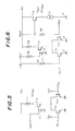
- FIG.6 is a circuit diagram of a first preferred embodiment of the present invention.
- a resistor R3, which is connected between the collector of the transistor Tr3 and the Vcc line, corresponds to the load element Lo shown in FIG.5.
- a resistor R1 is connected between the base of the transistor Tr1 and the Vcc line, and a resistor R2 is connected between the base of the transistor Tr2 and the Vcc line.
- the bias voltage V B1 applied to the base of the transistor Tr1 is generated by the resistor R1
- the bias voltage V B2 applied to the base of the transistor Tr2 is generated by the resistor R2.
- a resistor R4 is connected between the base of the transistor Tr3 and the Vcc line.
- the bias voltage V B3 is generated by the resistor R4.
- the output voltage obtained at the collector of the transistor Tr3 is amplified by an npn transistor Tr4, which has a base connected to the collector of the transistor Tr3, a collector connected to the Vcc line, and an emitter connected to the output terminal Tout.
- the collector of the transistor Tr3 has a high impedance and the emitter of the transistor Tr4 has a low impedance. That is, the output signal Vout is output to a subsequent-stage circuit (not shown) in the low-impedance state.
- the output signal Vout of the frequency conversion circuit shown in FIG.6 is output via the output terminal Tout.
- the output signal Vout includes a first signal component having a frequency equal to the sum of the frequencies of the input signals IN1 and IN2 and a second signal component having a frequency equal to the difference between the frequencies of the input signals IN1 and IN2.
- a constant-current source 2 is connected between the emitter of the transistor Tr4 and the ground G.
- FIG.7 is a circuit diagram of a frequency conversion circuit used in experiments.
- the bias voltage V B3 applied to the base of the transistor Tr3 is generated by resistors R4a and R4b connected in series between the Vcc line and the ground.
- a transistor Tr5 and a resistor R5 form the constant-current circuit 2 shown in FIG.6.
- Reference “RF” corresponds to the input signal IN1
- reference “LO” corresponds to the input signal IN2.
- Reference “IF” corresponds to the output signal Vout.
- the resistors R3, R4a, R4b and R5 have resistance values shown in FIG.7, and the capacitor C1 has a capacitance of 200pF.
- a bias circuit 10 generates a bias voltage of 1.22V from the power supply voltage Vcc.
- FIG.8 is a circuit diagram of an experimental system.
- An IC chip 100 includes the circuit shown in FIG.7, and eight terminals #1 - #8.
- An oscillator 101 generates a signal having a frequency of 1575MHz.
- the signal generated by the oscillator 101 is applied to terminal #1 via an LC circuit 105, which is biased by a variable DC source 103.
- An oscillator 102 generates a signal having a frequency of 1505MHz, which is applied to terminal #8 via an LC circuit 106 biased by a variable DC source 104.
- the variable DC source 103 generates a DC voltage VRF of 0.802V
- the variable DC source 104 generates a DC voltage of 0.7683V.
- a spectrum analyzer (not shown) is coupled to terminal #5 via a capacitor C11 having a capacitance of 1000pF.
- RF signal frequency 1575MHz
- LO signal frequency 1505MHz
- -10dBm IF signal frequency 70MHz.
- FIG.9A is a waveform diagram of the IF signal analyzed by the spectrum analyzer. It can be seen from FIG.9A that the IF signal has a frequency of 70MHz.
- FIG.9B is a graph showing a change in the output level of the 70MHz IF signal as the input level of the RF signal is changed in the state where the -10dBm LO signal having a frequency of 1505MHz is applied to terminal #8 (FIG.8).
- the conversion gain of the circuit shown in FIG.7 is equal to 13dB, and the output power (peak power: Pout) thereof is equal to -1.5dBm.
- a 1dB compression point CP which shows linearity of the circuit is at an output level of -6.54dBm and an input level of -18.8dBm.
- FIG.9C is a graph of input-output characteristics obtained when two RF signals respectively having frequencies of 1575MHz and 1575.1MHz are input to terminal #1.
- unwanted signal components plotted by crosses "x" appear in addition to the regular IF signal plotted by circles.
- Such unwanted signal components have frequencies (2f2 - f1) - f3 and (2f1 - f2) - f3 where f1 and f2 are the frequencies of the two RF signals, and f3 is the frequency of the LO signal.
- An intersect point IP3 where extension lines along linear portions of the two curves cross each other is at an output level of -8.35dBm and an input level of 3.56dBm.
- an isolation level from the RF signal side to the LO signal side is equal to -10dB, and an isolation level from the LO signal side to the RF signal side is equal to -15dB.
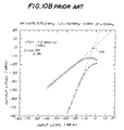
- FIGS.10A and 10B which correspond to FIGS.9B and 9C, respectively, are graphs showing the characteristics of the second conventional circuit shown in FIG.2.
- the conditions of measurements are the same as described previously except that the LO signal is at -5dBm.
- the conversion gain of the circuit shown in FIG.2 is equal to 8.7dB, and the output power (peak power: Pout) thereof is equal to -6.2dBm.
- the 1dB compression point CP is at an output level of -11.0dBm and an input level of -18.9dBm.
- unwanted signal components plotted by crosses "x" appear in addition to the regular IF signal plotted by circles.
- Such unwanted signal components have frequencies (2f2 - f1) - f3 and (2f1 - f2) - f3 where f1 and f2 are the frequencies of the two RF signals, and f3 is the frequency of the LO signal.
- the intersect point IP3 where extension lines along linear portions of the two curves cross each other is at an output level of 0.1dBm and an input level of -5.9dBm.
- the isolation level from the RF signal side to the LO signal side is equal to -27.2dB, and the isolation level from the LO signal side to the RF signal side is equal to -21.5dB.
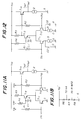
- FIG.11A is a circuit diagram of a second preferred embodiment of the present invention.
- the bias voltages V B1 , V B2 and V B3 respectively applied to the bases of the transistors Tr1, Tr2 and Tr3 are not generated from the power supply line Vcc but generated from a bias voltage generator separately from the power supply voltage Vcc.
- the bias voltages V B1 , V B2 and V B3 will vary if an AC component is superimposed on the Vcc line of the configuration shown in FIG.6.
- variations in the bias voltages V B1 , V B2 and V B3 are forward backed, and hence the circuit will oscillate.
- the circuit shown in FIG.11A does not have the above possibility.
- FIG.11B shows an example of the bias voltage generator.
- a resistor network consisting of resistors R6, R7 and R8 connected in series is connected between a Vcc' power supply line and the ground G.
- the Vcc' power supply line is a power supply system separated from the Vcc power supply line.
- a node where the resistors R6 and R7 are connected in series is connected to the resistor R4, and a node where the resistors R7 and R8 are connected in series is connected to the resistors R1 and R2.
- FIG.12 is a circuit diagram of a third preferred embodiment of the present invention.
- the emitters of the transistors Tr1 and Tr2 are grounded via constant-current sources 3.
- the constant-current sources 3 suppress variations in the collector currents of the transistors Tr1 and Tr2 from varying due to change in ambient temperature. AC signal components pass through the capacitors C2. With the above-mentioned arrangement, it becomes possible to improve the temperature characteristic of the circuit without degrading the high-frequency characteristic.
- FIG.13A is a circuit diagram of a fourth preferred embodiment of the present invention.
- An inductor L2 is substituted for the resistor R3 shown in FIG.6, and a series resonance circuit composed of an inductor L1 and a capacitor C3 is substituted for the capacitor C1.
- the power supply voltage Vcc is applied to the collector of the transistor Tr3 without any voltage drop.
- the circuit shown in FIG.13 has improved characteristics, as compared with the circuit shown in FIG.6.
- the series resonance circuit composed of the inductor L1 and the capacitor C3 has an impedance of zero at a resonant frequency.
- FIG.14 is a circuit diagram of a fifth preferred embodiment of the present invention.
- a transformer 4 which is substituted for the inductor L2 and the transistor Tr4 shown in FIG.13, functions as an impedance conversion element.
- the transformer 4 has a primary winding connected to the collector of the transistor Tr3 and the Vcc line, and a secondary winding connected to the Vcc line and the output terminal Tout.
- the transformer 4 converts a high impedance of the collector of the transistor Tr3 into a low impedance equal to, for example, 50 ⁇ .
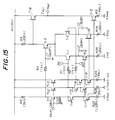
- FIG.15 is a circuit diagram of a practical application of the frequency conversion circuit of the present invention.
- a transistor Tr31 and a resistor R25 form the constant-current source 3 (FIG.12) connected to the emitter of the transistor Tr1.
- the constant-current source 3 connected to the emitter of the transistor Tr2 is composed of a transistor Tr32 and a resistor R26.
- the transistor Tr5 and the resistor R5 form the constant-current source shown in FIG.12.
- Transistors Tr11 - Tr19, resistors R21 - R24 and a capacitor C21 form a bias generator, which generates the bias voltages V B1 , V B2 and V B3 , and other bias voltages which will be described later.
- a predetermined bias voltage V BIAS equal to, for example, 2.8V, is applied to the bases of the transistors Tr11 - Tr13, which are grounded via the capacitor C21.
- a series circuit composed of diode-connected transistors Tr14 and Tr17 is connected to the emitter of the transistor Tr11, and grounded via the resistor R22.
- a series circuit composed of diode-connected transistors Tr15 and Tr18 is connected to the emitter of the transistor Tr12, and grounded via the resistor R23.
- a series circuit composed of diode-connected transistors Tr16 and Tr19 is connected to the emitter of the transistor Tr13, and grounded via the resistor R24. It should be noted that the bias voltages V B1 , V B2 and V B3 are not affected by variations in the power supply voltage Vcc (5V).
- the collectors of the transistors Tr15 and Tr16 are coupled to the bases of the transistors Tr1 and Tr2 via the resistors R1 and R2, respectively. Bias voltages applied to the bases of the transistors Tr31, Tr32 and Tr5 are generated at the collectors of the transistors Tr17, Tr18 and Tr19.
- FIG.16 is a variation of the first embodiment of the present invention shown in FIG.6.
- the npn transistors Tr1 - Tr4 shown in FIG.6 are replaced by pnp transistors.
- the circuit shown in FIG.16 operate in the same manner as the circuit shown in FIG.6.
- the circuit shown in FIG.16 is connected to the Vcc line (high-potential side) and the ground G. It is also possible to use a high-potential side power supply voltage equal to the ground level and a low-potential side power supply voltage V EE lower than the ground potential. It is possible to configure the other embodiments of the present invention by using pnp transistors.
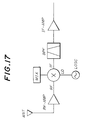
- the present invention can be applied to, for example, a radio communication device in a manner as shown in FIG.17, which shows a signal receiver part thereof.
- the signal receiver part is composed of an antenna ANT, a high-frequency low-noise amplifier RF-AMP, a mixer MIX, a local oscillator LOSC, a bandpass filter BPF and an intermediate frequency amplifier IF-AMP.
- the mixer MIX corresponds to the frequency conversion circuit of the present invention.
- the aforementioned RF signal via the high-frequency amplifier RF-AMP is applied to the mixer MIX, while the LO signal generated by the local oscillator LOSC is applied to the mixer MIX.
- the mixer MIX generates an IF (Intermediate Frequency) signal composed of a first signal component having a frequency equal to the sum of the frequencies of the RF signal and the LO signal and a second signal component having a frequency equal to the difference therebetween.
- the bandpass filter BPF functions to pass either the first signal component or the second signal component.
- the selected signal component is amplified by the intermediate frequency amplifier IF-AMP, and then supplied to a low-frequency amplifier (not shown) to which a speaker (not shown) is coupled.
- the RF signal has a frequency of, for example, 870MHz
- the LO signal has a frequency of, for example, 780MHz
- the IF signal has two frequency components of 90MHz and 1650MHz.
- the bandpass filter BPF passes only the 90MHz signal component.
Landscapes
- Engineering & Computer Science (AREA)
- Power Engineering (AREA)
- Amplifiers (AREA)
Applications Claiming Priority (2)
| Application Number | Priority Date | Filing Date | Title |
|---|---|---|---|
| JP2341009A JPH04208702A (ja) | 1990-11-30 | 1990-11-30 | 周波数変換回路 |
| JP341009/90 | 1990-11-30 |
Publications (1)
| Publication Number | Publication Date |
|---|---|
| EP0488257A1 true EP0488257A1 (de) | 1992-06-03 |
Family
ID=18342369
Family Applications (1)
| Application Number | Title | Priority Date | Filing Date |
|---|---|---|---|
| EP91120331A Withdrawn EP0488257A1 (de) | 1990-11-30 | 1991-11-26 | Frequenzumsetzungsschaltung |
Country Status (3)
| Country | Link |
|---|---|
| EP (1) | EP0488257A1 (de) |
| JP (1) | JPH04208702A (de) |
| KR (1) | KR920011049A (de) |
Cited By (5)
| Publication number | Priority date | Publication date | Assignee | Title |
|---|---|---|---|---|
| EP0715402A1 (de) * | 1994-11-29 | 1996-06-05 | Nec Corporation | Frequenzmischer mit geringem Übersprechen zwischen den Eingängen |
| EP1292018A3 (de) * | 2001-09-04 | 2003-07-23 | Kabushiki Kaisha Toshiba | Gegentakt-Mischer unter Verwendung von FETs |
| CN101882914A (zh) * | 2010-04-30 | 2010-11-10 | 苏州英诺迅科技有限公司 | 效率和线性度提高的功率放大器 |
| CN101882912A (zh) * | 2010-04-30 | 2010-11-10 | 苏州英诺迅科技有限公司 | 线性度和功率附加效率提高的射频cascode结构功率放大器 |
| CN101888214A (zh) * | 2010-04-30 | 2010-11-17 | 苏州英诺迅科技有限公司 | 效率和线性度提高的Cascode功率放大器 |
Citations (4)
| Publication number | Priority date | Publication date | Assignee | Title |
|---|---|---|---|---|
| GB2073983A (en) * | 1980-04-10 | 1981-10-21 | Pioneer Electronic Corp | Frequency conversion circuit |
| JPS6148205A (ja) * | 1984-08-16 | 1986-03-08 | Sony Corp | ミキサ |
| JPS61159893A (ja) * | 1984-12-31 | 1986-07-19 | Nec Home Electronics Ltd | ビデオテ−プレコ−ダ |
| JPH02151178A (ja) * | 1988-12-02 | 1990-06-11 | Sony Corp | 直流分カット回路 |
-
1990
- 1990-11-30 JP JP2341009A patent/JPH04208702A/ja active Pending
-
1991
- 1991-11-26 EP EP91120331A patent/EP0488257A1/de not_active Withdrawn
- 1991-11-29 KR KR1019910021729A patent/KR920011049A/ko not_active Ceased
Patent Citations (4)
| Publication number | Priority date | Publication date | Assignee | Title |
|---|---|---|---|---|
| GB2073983A (en) * | 1980-04-10 | 1981-10-21 | Pioneer Electronic Corp | Frequency conversion circuit |
| JPS6148205A (ja) * | 1984-08-16 | 1986-03-08 | Sony Corp | ミキサ |
| JPS61159893A (ja) * | 1984-12-31 | 1986-07-19 | Nec Home Electronics Ltd | ビデオテ−プレコ−ダ |
| JPH02151178A (ja) * | 1988-12-02 | 1990-06-11 | Sony Corp | 直流分カット回路 |
Non-Patent Citations (5)
| Title |
|---|
| GAAS IC SYMPOSIUM, NOV 12-14, 1985, MONTEREY, CALIFORNIA, TECHNICAL DIGEST November 1985, NEW YORK, USA pages 165 - 168; DAUTRICHE ET AL.: 'GaAs MONOLITHIC CIRCUITS FOR TV TUNERS' * |
| PATENT ABSTRACTS OF JAPAN (E-461)5 December 1986 & JP-A-61 159 893 ( NEC HOME ELECTRONICS LTD ) 19 July 1986 * |
| PATENT ABSTRACTS OF JAPAN vol. 10, no. 205 (E-420)17 July 1986 & JP-A-61 048 205 ( SONY CORPORATION ) 8 March 1986 * |
| PATENT ABSTRACTS OF JAPAN vol. 14, no. 401 (E-971)30 August 1990 & JP-A-2 151 178 ( SONY CORPORATION ) 11 June 1990 * |
| PATENT ABSTRACTS OF JAPAN vol. 7, no. 8 (E-152)(1153) 13 January 1983 * |
Cited By (8)
| Publication number | Priority date | Publication date | Assignee | Title |
|---|---|---|---|---|
| EP0715402A1 (de) * | 1994-11-29 | 1996-06-05 | Nec Corporation | Frequenzmischer mit geringem Übersprechen zwischen den Eingängen |
| EP1292018A3 (de) * | 2001-09-04 | 2003-07-23 | Kabushiki Kaisha Toshiba | Gegentakt-Mischer unter Verwendung von FETs |
| US6954089B2 (en) | 2001-09-04 | 2005-10-11 | Kabushiki Kaisha Toshiba | Frequency converter having low supply voltage |
| US7075345B2 (en) | 2001-09-04 | 2006-07-11 | Kabushiki Kaisha Toshiba | Frequency converter having low supply voltage |
| US7123061B2 (en) | 2001-09-04 | 2006-10-17 | Kabushiki Kaisha Toshiba | Frequency converter having low supply voltage |
| CN101882914A (zh) * | 2010-04-30 | 2010-11-10 | 苏州英诺迅科技有限公司 | 效率和线性度提高的功率放大器 |
| CN101882912A (zh) * | 2010-04-30 | 2010-11-10 | 苏州英诺迅科技有限公司 | 线性度和功率附加效率提高的射频cascode结构功率放大器 |
| CN101888214A (zh) * | 2010-04-30 | 2010-11-17 | 苏州英诺迅科技有限公司 | 效率和线性度提高的Cascode功率放大器 |
Also Published As
| Publication number | Publication date |
|---|---|
| KR920011049A (ko) | 1992-06-27 |
| JPH04208702A (ja) | 1992-07-30 |
Similar Documents
| Publication | Publication Date | Title |
|---|---|---|
| US6392492B1 (en) | High linearity cascode low noise amplifier | |
| US5995814A (en) | Single-stage dual-band low-noise amplifier for use in a wireless communication system receiver | |
| US6967528B2 (en) | Variable gain amplifier | |
| KR100427878B1 (ko) | 증폭회로 | |
| US7109796B2 (en) | Amplifying circuit with adjustable amplification and transmitter system comprising such an amplifying circuit | |
| US6304145B1 (en) | Large signal amplifier gain compensation circuit | |
| JPH04352507A (ja) | 増幅器 | |
| US5307026A (en) | Variable gain RF amplifier with linear gain control | |
| US5378997A (en) | Low noise amplifier with capacitive feedback | |
| EP1639699B1 (de) | Schaltungsanordnung zur detektion der ausgangsleistung | |
| US6922556B2 (en) | System and method for establishing a bias current using a feedback loop | |
| US6744308B1 (en) | System and method for establishing the input impedance of an amplifier in a stacked configuration | |
| EP0488257A1 (de) | Frequenzumsetzungsschaltung | |
| KR100371876B1 (ko) | 주파수 변환회로 | |
| EP1670137A1 (de) | Hochfrequenzverstärker | |
| EP1401097B1 (de) | Fm-antennenverstärker | |
| JP3105846B2 (ja) | 広帯域電力増幅器 | |
| US6208205B1 (en) | Amplifier circuit and method for reducing noise therein | |
| CN100471040C (zh) | 起动信号输出电路 | |
| US6995610B2 (en) | Amplifier and radio frequency tuner | |
| US20240022218A1 (en) | Analog amplitude pre-distortion circuit and method | |
| JPS5922416A (ja) | 高周波増幅回路 | |
| JPH0653761A (ja) | 高周波増幅器 | |
| JPS62100010A (ja) | 対数増幅器 | |
| JP3400911B2 (ja) | ゲートバイアス電圧生成回路 |
Legal Events
| Date | Code | Title | Description |
|---|---|---|---|
| PUAI | Public reference made under article 153(3) epc to a published international application that has entered the european phase |
Free format text: ORIGINAL CODE: 0009012 |
|
| AK | Designated contracting states |
Kind code of ref document: A1 Designated state(s): DE FR GB |
|
| STAA | Information on the status of an ep patent application or granted ep patent |
Free format text: STATUS: THE APPLICATION IS DEEMED TO BE WITHDRAWN |
|
| 18D | Application deemed to be withdrawn |
Effective date: 19930215 |