EP0488442B1 - Commande automatique d'exposition pour une image divisée en zones - Google Patents
Commande automatique d'exposition pour une image divisée en zones Download PDFInfo
- Publication number
- EP0488442B1 EP0488442B1 EP91202996A EP91202996A EP0488442B1 EP 0488442 B1 EP0488442 B1 EP 0488442B1 EP 91202996 A EP91202996 A EP 91202996A EP 91202996 A EP91202996 A EP 91202996A EP 0488442 B1 EP0488442 B1 EP 0488442B1
- Authority
- EP
- European Patent Office
- Prior art keywords
- area
- zone
- zones
- specific
- adjacent
- Prior art date
- Legal status (The legal status is an assumption and is not a legal conclusion. Google has not performed a legal analysis and makes no representation as to the accuracy of the status listed.)
- Expired - Lifetime
Links
Images



Classifications
-
- G—PHYSICS
- G03—PHOTOGRAPHY; CINEMATOGRAPHY; ANALOGOUS TECHNIQUES USING WAVES OTHER THAN OPTICAL WAVES; ELECTROGRAPHY; HOLOGRAPHY
- G03B—APPARATUS OR ARRANGEMENTS FOR TAKING PHOTOGRAPHS OR FOR PROJECTING OR VIEWING THEM; APPARATUS OR ARRANGEMENTS EMPLOYING ANALOGOUS TECHNIQUES USING WAVES OTHER THAN OPTICAL WAVES; ACCESSORIES THEREFOR
- G03B7/00—Control of exposure by setting shutters, diaphragms or filters, separately or conjointly
- G03B7/28—Circuitry to measure or to take account of the object contrast
-
- H—ELECTRICITY
- H04—ELECTRIC COMMUNICATION TECHNIQUE
- H04N—PICTORIAL COMMUNICATION, e.g. TELEVISION
- H04N23/00—Cameras or camera modules comprising electronic image sensors; Control thereof
- H04N23/70—Circuitry for compensating brightness variation in the scene
- H04N23/75—Circuitry for compensating brightness variation in the scene by influencing optical camera components
-
- H—ELECTRICITY
- H04—ELECTRIC COMMUNICATION TECHNIQUE
- H04N—PICTORIAL COMMUNICATION, e.g. TELEVISION
- H04N23/00—Cameras or camera modules comprising electronic image sensors; Control thereof
- H04N23/70—Circuitry for compensating brightness variation in the scene
-
- H—ELECTRICITY
- H04—ELECTRIC COMMUNICATION TECHNIQUE
- H04N—PICTORIAL COMMUNICATION, e.g. TELEVISION
- H04N23/00—Cameras or camera modules comprising electronic image sensors; Control thereof
- H04N23/70—Circuitry for compensating brightness variation in the scene
- H04N23/71—Circuitry for evaluating the brightness variation
Definitions
- the present invention relates to an automatic exposure controlling method suitable for use in a camera device such as a video camera and also to an apparatus for implementing such a method.
- An automatic exposure controlling method is characterized by dividing the picturing area into a specific zone and a plurality of zones adjacent to said specific zone; calculating an average luminance of each image in said specific and adjacent zones; with respect to each combination of said specific zone with a respective one of said plurality of zones, calculating a difference in average luminance between the two zones, moving a boundary between the specific zone and the adjacent zone towards this adjacent zone when said difference is not greater than a specific value, and moving said boundary away from said adjacent zone when said difference is greater than said specific value; and applying a maximum weight to the average luminance in said specific zone and controlling the iris based principally on this weighted average luminance.
- the position of the above specific zone follows a subject within the picturing area and the shape of the zone is also rendered very similar to that of the subject. It is therefore possible to carry out an accurate exposure control in response to the luminance of a subject.
- An automatic exposure control apparatus is characterized by comprising storage means for storing coordinates each of which defines a boundary between a specific zone and a respective one of plural zones adjacent to said specific zone in the picturing area; calculating means for calculating an average luminance of an image in each zone based on information representative of luminance of a picture in the picturing area and said coordinates; changing means, with respect to each combination of said specific zone with a respective one of said plural zones, for calculating a difference in average luminance between the specific zone and the adjacent zone to change the corresponding coordinate so that the boundary between the specific zone and the adjacent zone moves towards this adjacent zone when said difference is not greater than a specific value and to change said corresponding coordinate so that said boundary moves away from said adjacent zone when said difference is greater than said specific value; applying means for applying a maximum weight to that part of said information representative of the luminance of the picture within said picturing area which corresponds to said specific zone based on said coordinates; and control means for controlling opening of the iris in accordance with an output from said weight applying means.
- the apparatus of the above structure may further be provided with means for outputting a signal corresponding to an area size of the specific zone in accordance with the coordinates so that the control means control the opening of an iris in response to an output of the weight applying means and the signal corresponding to the area size.
- Fig. 1 shows a picturing area S in this automatic exposure controlling method.
- the picturing area S is divided, for example, into five sub-areas A1, A2, A3, A4 and A5 wherein the central sub-area A3 is a luminance measuring zone which is given a larger weight than the other sub-areas.
- the central sub-area A3 is a luminance measuring zone which is given a larger weight than the other sub-areas.
- an average luminance of the image is obtained.
- a difference between the average luminance of the above central sub-area A3 and that of a respective one of the sub-areas A1, A2, A4 and A5 adjacent to the sub-area A3 is obtained.
- the central sub-area A3 is expanded towards the relevant adjacent sub-area, and if the difference in average luminance exceeds the predetermined value the central sub-area A3 is reduced on the side of the relevant adjacent sub-area.
- the average luminance values of the areas A3 and A4 are both high and those of the areas A1, A2 and A5 are similar and low. Therefore, the central sub-area A3 is expanded on the side of the sub-area A4 and is reduced on the sides of the sub-areas A1, A2 and A5, which results in the state shown in Fig. 3
- this sub-area follows a target subject, so that a bright or a dark background which is different in luminance from the subject is excluded from this sub-area A3. Therefore, if the iris is controlled in accordance with the luminance in the thus obtained central sub-area A3, an exposure state suitable for shooting the subject S2 can be obtained.
- Fig. 4 shows the structure of an embodiment of the automatic exposure control apparatus which is applied to a video camera.
- optical picture information received via a camera lens 10 passes through an iris 11 and reaches an image sensor 12 which is constructed comprising a CCD.
- This image sensor 12 converts the optical picture information into an electric picture signal corresponding thereto in response to a timing signal fed from a timing generator circuit 13 in the known scanning manner.
- This picture signal is supplied to an automatic gain control circuit (AGC circuit) 14, an analog-to-digital converter (A/D converter) 15 and a weighting circuit 16.
- AGC circuit automatic gain control circuit
- A/D converter analog-to-digital converter
- the AGC circuit 14 amplifies the picture signal so that an output of a constant amplitude is obtained and supplies the amplified signal to a picture signal processing circuit 17.
- This picture signal processing circuit 17 performs a predetermined processing on the received picture signal and then supplies the processed signal to relevant portions of this video camera such as a video signal encoder (not shown).
- the A/D converter 15 samples the luminance component of the picture signal fed from the image sensor 12, for example, at a frequency 64f H sixty four times as high as the horizontal scanning frequency based on an output of the timing generator circuit 13 and converts each sample into a digital value.
- the thus obtained digital luminance values are supplied in succession to an accumulator circuit 18.
- This accumulator circuit 18 accumulates the digital luminance values with regard to each of the sub-areas A1 to A5, for example, for each field period in accordance with an output of a gating signal generating circuit 19 which will be described later.
- the respective accumulated values thus obtained are supplied to a processor 20 which is constituted, for example, by a microcomputer or the like.
- programs for carrying out calculations and various controls including the control of the gating signal generating circuit 19, addresses on the picturing area and the like have previously been stored.
- the gating signal generating circuit 19 generates a gating signal G1 corresponding to the scanning period of the sub-area A1, a gating signal G2 corresponding to the scanning period of the sub-area A2, a gating signal G3 corresponding to the scanning period of the sub-area A3, a gating signal G4 corresponding to the scanning period of the sub-area A4, a gating signal G5 corresponding to the scanning period of the sub-area A5 and other necessary timing signals.
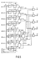
- This circuit may be constructed as shown in Fig. 5.
- an output bus 30 of the aforesaid processor 20 is connected to eight registers R1 to R8.
- the registers R1, R2, R3 and R4 are loaded by the processor 20 with addresses Y1 (representing the upper end of the sub-area A1, see Fig. 1), Y2 (the lower end of the sub-area A1), Y3 (the upper end of the sub-area A5) and Y4 (the lower end of the sub-area A5) on the picturing area S each in the form of two's complement in response respectively to signals W1, W2, W3 and W4 supplied from the processor.
- the registers R5, R6, R7 and R8 are loaded with addresses X1 (the left-hand end of the sub-area A2), X2 (the right-hand end of the sub-area A2), X3 (the left-hand end of the sub-area A4) and X4 (the right-hand end of the sub-area A4) on the area S each in the form of two's complement.
- Output terminals of these registers R1 to R8 are connected to data input terminals of counters C1 to C8, respectively.
- Load terminals L of the counters C1 to C4 are supplied by the timing signal generator circuit 13 with a vertical synchronization signal VS.
- the addresses Y1 to Y4 in the registers R1 to R4 are loaded into the counters C1 to C4, respectively.
- Clock terminals C of the counters C1 to C4 are supplied by the timing signal generator circuit 13 with a horizontal synchronization signal HS. Each time the signal HS is generated, the contents of the counters C1 to C4 are incremented.
- a carry output terminal of the counter C1 is connected to a set terminal of a flip-flop FY12, and a carry output terminal of the counter C2 is connected to a reset terminal of the same flip-flop.
- this flip-flop FY12 is brought into a set state when the counter C1 outputs a carry and is brought into a reset state when the counter C2 outputs a carry.
- flip-flops FY23 and FY34 are brought into set states respectively by carries from the counters C2 and C3 and brought into reset states respectively by carries from the counters C3 and C4.
- the counters C5 to C8 are supplied at their load terminals L with the horizontal synchronization signal HS. When this signal HS is generated, the addresses X1 to X4 in the registers R5 to R8 are loaded into the counters C5 to C8, respectively.
- the counters C5 to C8 are also supplied at their clock terminals C with the timing signal 64f H . Each time this signal 64f H is generated, the contents of these counters are incremented.
- Flip-flops FX12, FX23, FX34 and FX14 are brought into set states respectively by carry outputs of the counters C5, C6, C7 and C5 and are brought into reset states respectively by carry outputs of the counters C6, C7, C8 and C8 in a manner described above for the flip-flops FY12 to FY34.
- An output signal Y12 of the flip-flop FY12 is supplied to one input terminal of an AND gate 31, to the other input terminal of which an output signal X14 of the flip-flop FX14 is supplied.
- this AND gate 31 outputs a gating signal G1 which becomes true during the time when the sub-area A1 is scanned.
- An output signal Y23 of the flip-flop FY23 is supplied to one input terminals of AND gates 32 to 34.
- the other input terminal of the AND gate 32 is supplied with an output X12 of the flip-flop FX12, so that this AND gate outputs a gating signal G2 which becomes true during the time when the sub-area A2 is scanned.
- the other input terminal of the AND gate 33 is supplied with an output X23 of the flip-flop FX23, so that this AND gate outputs a gating signal G3 which becomes true during the time when the sub-area A3 is scanned.
- an AND gate 34 produces from the signal signal Y23 and an output signal X34 of the flip-flop FX34 a gating signal G4 which becomes true during the scanning period of the sub-area A4, and an AND gate 35 produces from the signal X14 and an output signal Y34 of the flip-flop FY34 a gating signal G5 which becomes true during the scanning period of the sub-area A5.
- the gating signals G1 to G5 are supplied to the accumulator circuit 18 shown in Fig. 4. This accumulator circuit 18 may be constructed as shown in Fig. 6.
- the gating signals G1 to G5 are supplied one input terminals of AND gates 41 to 45, respectively.
- the other input terminals of these AND gates are supplied with the timing signal 64f H , so that each AND gate outputs the timing signal 64f H only when a respective one of the sub-areas A1 to A5 is scanned.
- the digital luminance values (the sample values) sequentially outputted from the A/D converter 15 shown in Fig. 4 are supplied to a data input terminal of a latch circuit 46 and are loaded in succession into this latch circuit in response to the timing signal 64f H .
- the digital luminance value outputted from the latch circuit 46 is supplied to one input terminal of an adder 47 and is added in this adder to a value fed to the other input terminal thereof, the addition result being supplied to respective data input terminals of latch circuits 51 to 55.
- Clock input terminals of these latch circuits 51 to 55 are supplied with output signals of the AND gates 41 to 45, respectively. Therefore, each of the latch circuits 51 to 55 latches the output values of the adder 47 and supplies them to a respective one of buffer amplifiers 61 to 65 in the subsequent stage only when a relevant one of the sub-areas A1 to A5 is scanned.
- Each of the buffer amplifiers 61 to 65 supplies an output of a corresponding one of the latch circuits 51 to 55 to the other input terminal of the adder 47 only when a respective one of the gating signals G1 to G5 is true.
- the latch circuits 51 to 55 are supplied at their clear terminals with the vertical synchronization signal VS.
- the latch circuits 51 to 55 are first cleared by the vertical synchronization signal VS and thereafter the digital luminance values received from the A/D converter 15 are successively supplied to the adder 47 at the time interval of the signal 64f H .
- the signal G1 is true, so that the output of the adder 47 is fed back to the other data input terminal of this adder through the latch circuit 51 and the buffer amplifier 61, whereby an accumulator circuit is formed.
- an accumulated value of the digital luminance values produced during the scanning period of the sub-area A1 is obtained at the latch circuit 51.
- accumulated values of the digital luminance values produced during the respective scanning periods of the sub-areas A2, A3, A4 and A5 are obtained at the latch circuits 52, 53, 54 and 55, respectively.
- the processor 20 shown in Fig. 4 sequentially enables the buffer amplifiers 61 to 65 by a not-shown timing signal so that the respective accumulated values contained in the latch circuits 51 to 55 are read out through an input bus 66 and are stored.
- the gating signal G3 generated by the gating signal generating circuit 19 is further supplied to the weighting circuit 16.
- This weighting circuit is of the conventional structure and supplies, over the time period when the gating signal G3 is generated, the luminance component of the picture signal from the image sensor 12 to a low-pass filter 70 after applying a predetermined weight to this luminance component.
- the low-pass filter 70 smoothes the received signal and supplies it to a non-inverting input terminal of an operational amplifier 72 provided in an iris control circuit 71.
- the operational amplifier performs a control in such a way that the opening of the iris 11 changes in the closing sense when the output voltage of this amplifier increases and changes in the opening sense when the output voltage decreases.
- the processor 20 reads the accumulated digital luminance values in the respective sub-areas from the accumulator circuit 18 each time the scanning, for example, of each field of the taken picture ends.
- the processor 20 also calculates area sizes of the sub-areas based on the addresses Y1 to Y4 and X1 to X4 which define these sub-areas.
- the processor 20 then obtain the average luminance values L(1) to L(5) in the sub-areas A1 to A5 by dividing the accumulated luminance values by the relevant area sizes, respectively.
- the processor 20 further determines the maximum value L(max) and the minimum value L(min) of the average luminance values L(1) to L(5) and also calculates an average value L(mean) of these average luminance values.
- the processor 20 determines the following relation between the average luminance L(3) of the sub-area A3 disposed centrally of the picture area S and those of the sub-areas A1, A2, A4 and A5 adjoining this central sub-area:
- ⁇ C 1 ⁇ L(max) - L(min) where i is an integer of 1, 2, 4 or 5, C 1 being a predetermined constant.
- the processor 20 then carries out further processing. More specifically, when the above formula (1) is established the relevant one of the addresses X1 to X4 and Y1 to Y4 are changed to move the boundary between the central sub-area A3 and the sub-area Ai towards the sub-area Ai.
- the boundary is moved away from the sub-area Ai.
- the address X3 disposed on the boundary between the sub-areas A3 and A4 is increased to thereby move the boundary towards the sub-area A4, that is to say, in the right-hand direction.
- the address X2 is increased to move the boundary between these sub-areas away from the sub-area A2, that is to say, in the right-hand direction. The same is true of the other sub-areas.
- the central sub-area A3 is expanded on the side of that adjacent sub-area whose difference in average luminance from the sub-area A3 is small and is decreased on the side of that adjacent sub-area whose difference in average luminance is large.
- the processor 20 outputs to a D/A converter 73 a value which is correspondent to (for example, in proportion to) the area size of the central sub-area A3.
- the D/A converter 73 in turn converts the above value into an analog signal which is supplied to an inverting input terminal of the operational amplifier 72 as a reference signal.
- the reference signal to be compared at the iris control circuit 71 with the output from the low-pass filter 70 is varied in accordance with the area size of the central sub-area A3, that is to say, in accordance with the size of a subject in the picturing area.
- the reason for this is as follows.
- the output value of the low-pass filter 70 is high when a subject has a large area and low when a subject has a small area even if the subjects have the same luminance. Therefore, if the value of the reference signal to be compared with this output is changed in accordance with the area size of a subject, substantially the same opening of the iris can be obtained with regard to subjects having the same luminance irrespectively of area sizes thereof.
- an output of a circuit shown, for example, in Fig. 7 may selectively be mixed through a switch element or the like with the video signal which is supplied to an electronic viewfinder (not shown) of this video camera so that the boundary of the sub-area A3 is displayed on a screen of the viewfinder in the form of a window frame.
- the circuit shown in Fig. 7 is constructed comprising an AND gate 81 which receives the signals Y2 and X23 from the gating signal generating circuit 19 and an AND gate 82 which receives the signals Y3 and X23.
- This circuit further comprises an AND gate 83 which receives the signals X2 and Y23, an AND gate 84 which receives the signals X3 and Y23 and an OR gate 85 which receives outputs from the above four AND gates.
- the picturing area S is divided as shown in Fig. 1.
- the way of dividing the picturing area should not be restricted only to this, but it will be apparent that the division may alternatively be performed in such a way that the picturing area is rotated by ninety degrees in Fig. 1 or in other ways.
- the way of determination about the difference in average luminance between the central sub-area and the adjacent sub-areas should not be restricted only to those represented by the above formulas (1) and (2), and other determination methods may be employed.
- the way of changing the weight in accordance with the area size of the central sub-area A3 should not also be restricted only to that shown in Fig. 4.
- an output signal of the D/A converter 73 may be supplied to the weighting circuit 16 as indicated by a broken line in Fig. 4.
- the weighting circuit 16 should be constructed such that the weight to be applied therein is changed in response to the above signal, and the inverting input terminal of the operational amplifier 72 should be supplied with a fixed reference voltage V ref .
- the minimum values of the addresses X2 and Y2 and the maximum values of the addresses X3 and Y3 may be set to desired values, respectively.
Landscapes
- Engineering & Computer Science (AREA)
- Multimedia (AREA)
- Signal Processing (AREA)
- Physics & Mathematics (AREA)
- General Physics & Mathematics (AREA)
- Exposure Control For Cameras (AREA)
- Transforming Light Signals Into Electric Signals (AREA)
- Studio Devices (AREA)
Claims (6)
- Procédé de commande automatique de l'ouverture d'un iris sur la base principalement de la luminance d'une image dans une zone spécifique à l'intérieur d'une zone de formation d'image, caractérisé en ce que :on divise la zone de formation d'image en une zone spécifique et en une pluralité de zones voisines de ladite zone spécifique,on calcule une luminance moyenne de chaque image dans lesdites zones spécifique et voisines,on calcule, par rapport à chaque combinaison de ladite zone spécifique avec une zone respective de ladite pluralité de zones, une différence de luminance moyenne entre les deux zones, on déplace une limite, entre la zone spécifique et la zone voisine, vers cette zone voisine, lorsque ladite différence n'est pas supérieure à une valeur spécifique, on éloigne ladite limite de ladite zone voisine lorsque ladite différence est supérieure à ladite valeur spécifique, eton applique une pondération maximum à la luminance moyenne de ladite zone spécifique et on commande l'iris principalement sur la base de cette luminance moyenne pondérée.
- Procédé selon la revendication 1, caractérisé en ce que ladite zone spécifique est étendue vers toutes les zones voisines de ladite pluralité lorsqu'une différence entre la valeur maximum et la valeur minimum des valeurs de luminance moyennes de ladite zone spécifique et desdites zones voisines est inférieure à une valeur spécifique.
- Procédé selon la revendication 1 ou 2, caractérisé en ce que ladite pondération maximum est modifiée en fonction de la surface de ladite zone spécifique.
- Appareil de commande d'ouverture automatique d'un iris basé principalement sur la luminance d'une image dans une zone spécifique à l'intérieur d'une zone de formation d'image, caractérisé par la présence :de moyens de stockage pour stocker des coordonnées dont chacune définit une limite entre une zone spécifique et une zone respective de plusieurs zones voisines de ladite zone spécifique dans la zone de formation d'image,de moyens de calcul pour calculer une luminance moyenne d'une image dans chaque zone sur la base d'informations représentatives de la luminance d'une image dans la zone de formation d'image et desdites coordonnées,de moyens de changement, par rapport à chaque combinaison de ladite zone spécifique avec une zone respective desdites plusieurs zones, pour calculer une différence de luminance moyenne entre la zone spécifique et la zone voisine afin de modifier la coordonnée correspondante de telle sorte que la limite entre la zone spécifique et la zone voisine se déplace vers cette zone voisine lorsque ladite différence n'est pas supérieure à une valeur spécifique et pour modifier ladite coordonnée correspondante de telle manière que ladite limite s'écarte de ladite zone voisine lorsque ladite différence est supérieure à ladite valeur spécifique,de moyens d'application pour appliquer, sur la base desdites coordonnées, une pondération maximum à la partie desdites informations représentatives de la luminance de l'image à l'intérieur de ladite zone de formation d'image, qui correspond à ladite zone spécifique, etde moyens de commande pour commander l'ouverture de l'iris en fonction d'une sortie desdits moyens d'application de pondération.
- Appareil selon la revendication 4, caractérisé en ce que sont en outre prévus des moyens de sortie pour délivrer un signal correspondant à une surface de ladite zone spécifique basée sur lesdites coordonnées, lesdits moyens de commande commandant l'ouverture dudit iris en fonction dudit signal correspondant à la surface et à la sortie desdits moyens d'application de pondération.
- Appareil selon la revendication 4 ou 5, caractérisé en ce que lesdits moyens de calcul de la luminance moyenne comprennent des moyens générateurs de signaux de déclenchement pour générer des signaux de déclenchement correspondant respectivement auxdites zones sur la base desdites coordonnées, des moyens d'accumulation pour accumuler des valeurs d'échantillonnage des informations de luminance de l'image dans ladite zone de formation d'image par rapport à chacune desdites zones en fonction desdits signaux de déclenchement, et des moyens de division pour diviser des valeurs accumulées délivrées par lesdits moyens d'accumulation, respectivement, par des surfaces desdites zones dérivées desdites coordonnées pour ainsi obtenir la luminance moyenne des zones respectives.
Applications Claiming Priority (2)
| Application Number | Priority Date | Filing Date | Title |
|---|---|---|---|
| JP2327413A JP2979081B2 (ja) | 1990-11-28 | 1990-11-28 | 自動露光制御方法及び装置 |
| JP327413/90 | 1990-11-28 |
Publications (3)
| Publication Number | Publication Date |
|---|---|
| EP0488442A2 EP0488442A2 (fr) | 1992-06-03 |
| EP0488442A3 EP0488442A3 (en) | 1993-06-09 |
| EP0488442B1 true EP0488442B1 (fr) | 1997-03-05 |
Family
ID=18198881
Family Applications (1)
| Application Number | Title | Priority Date | Filing Date |
|---|---|---|---|
| EP91202996A Expired - Lifetime EP0488442B1 (fr) | 1990-11-28 | 1991-11-19 | Commande automatique d'exposition pour une image divisée en zones |
Country Status (5)
| Country | Link |
|---|---|
| US (1) | US5184172A (fr) |
| EP (1) | EP0488442B1 (fr) |
| JP (1) | JP2979081B2 (fr) |
| KR (1) | KR100192857B1 (fr) |
| DE (1) | DE69124941T2 (fr) |
Families Citing this family (25)
| Publication number | Priority date | Publication date | Assignee | Title |
|---|---|---|---|---|
| DE69231428T2 (de) * | 1991-02-13 | 2001-01-18 | Nikon Corp., Tokio/Tokyo | Belichtungsrechner |
| US5392091A (en) * | 1991-08-27 | 1995-02-21 | Nikon Corporation | Exposure calculating apparatus |
| JP3170722B2 (ja) * | 1991-09-03 | 2001-05-28 | 株式会社ニコン | 露出演算装置 |
| US5694168A (en) * | 1991-09-04 | 1997-12-02 | Fuji Photo Film Co., Ltd. | Auto focus control device and method including selecting a zone for detecting an evaluative value for focusing in accordance with photographing direction |
| JP3131025B2 (ja) * | 1992-06-08 | 2001-01-31 | キヤノン株式会社 | ビデオカメラ及びその制御方法 |
| JP3456215B2 (ja) * | 1992-07-06 | 2003-10-14 | 株式会社ニコン | カメラの測光装置 |
| US5621462A (en) * | 1992-08-18 | 1997-04-15 | Canon Kabushiki Kaisha | Image pickup device capable of controlling made pickup operation |
| US5450163A (en) * | 1992-09-25 | 1995-09-12 | Nikon Corporation | Photometric device for camera |
| US5541706A (en) * | 1992-10-22 | 1996-07-30 | Nikon Corporation | Exposure calculation device for a camera |
| DE4417234C2 (de) * | 1993-05-17 | 2002-01-17 | Asahi Optical Co Ltd | Fotometriesystem |
| JP3035434B2 (ja) * | 1993-10-13 | 2000-04-24 | キヤノン株式会社 | 複眼撮像装置 |
| JP2809081B2 (ja) * | 1993-12-27 | 1998-10-08 | 日本電気株式会社 | 露光装置 |
| US6509927B1 (en) | 1994-12-16 | 2003-01-21 | Hyundai Electronics America Inc. | Programmably addressable image sensor |
| KR0160191B1 (ko) * | 1995-08-12 | 1999-01-15 | 김광호 | 역광보정방법 및 그 장치 |
| KR100388918B1 (ko) * | 1995-09-29 | 2003-09-13 | 삼성테크윈 주식회사 | 카메라의측광영역이가변되는휘도측광장치및그제어방법 |
| DE19701484A1 (de) * | 1997-01-17 | 1998-07-23 | Bosch Gmbh Robert | Verfahren zur Regelung der Belichtung von Videokameras |
| JP3892172B2 (ja) | 1998-07-24 | 2007-03-14 | 松下電器産業株式会社 | 固体撮像装置 |
| US7136098B1 (en) | 1998-10-23 | 2006-11-14 | Smith & Nephew, Inc. | Image illumination optimizing |
| JP3938833B2 (ja) * | 2000-04-27 | 2007-06-27 | 株式会社リコー | 露出制御装置 |
| US6958778B2 (en) * | 2000-11-21 | 2005-10-25 | Hitachi Kokusai Electric Inc. | Iris control method and apparatus for television camera for controlling iris of lens according to video signal, and television camera using the same |
| KR20040033967A (ko) * | 2002-10-16 | 2004-04-28 | 삼성테크윈 주식회사 | 지정 검출 영역의 위치가 변하는 디지털 카메라의 제어 방법 |
| JP4289259B2 (ja) * | 2004-08-31 | 2009-07-01 | カシオ計算機株式会社 | 撮像装置及び露出制御方法 |
| DE102006007092A1 (de) * | 2005-03-01 | 2006-09-07 | Denso Corp., Kariya | Bildgebungsvorrichtung |
| CN100373927C (zh) * | 2005-03-21 | 2008-03-05 | 王美娟 | 数字摄影装置的自动曝光方法 |
| US7398016B2 (en) * | 2005-11-04 | 2008-07-08 | Seiko Epson Corporation | Backlight compensation using threshold detection |
Family Cites Families (8)
| Publication number | Priority date | Publication date | Assignee | Title |
|---|---|---|---|---|
| JPS5652732A (en) * | 1979-10-05 | 1981-05-12 | Fuji Photo Film Co Ltd | Exposure control method |
| US4445778A (en) * | 1979-12-21 | 1984-05-01 | Fuji Photo Film Co., Ltd. | Method of and apparatus for measuring scene brightness |
| US4534639A (en) * | 1982-12-21 | 1985-08-13 | Canon Kabushiki Kaisha | Camera having an exposure mode change-over device |
| JPS61279829A (ja) * | 1985-06-06 | 1986-12-10 | Canon Inc | 測光装置を有するカメラ |
| US4855780A (en) * | 1987-05-22 | 1989-08-08 | Canon Kabushiki Kaisha | Photometric device for pseudo format camera |
| US4929824A (en) * | 1988-02-26 | 1990-05-29 | Fuji Photo Film Co., Ltd. | light metering device with detector matrix and mean value detection |
| GB2219461B (en) * | 1988-05-02 | 1992-11-18 | Canon Kk | Exposure control device |
| US4978990A (en) * | 1988-10-04 | 1990-12-18 | Olympus Optical Co., Ltd. | Exposure control apparatus for camera |
-
1990
- 1990-11-28 JP JP2327413A patent/JP2979081B2/ja not_active Expired - Fee Related
-
1991
- 1991-10-02 US US07/771,386 patent/US5184172A/en not_active Expired - Fee Related
- 1991-11-19 EP EP91202996A patent/EP0488442B1/fr not_active Expired - Lifetime
- 1991-11-19 DE DE69124941T patent/DE69124941T2/de not_active Expired - Fee Related
- 1991-11-25 KR KR1019910021060A patent/KR100192857B1/ko not_active Expired - Fee Related
Also Published As
| Publication number | Publication date |
|---|---|
| EP0488442A3 (en) | 1993-06-09 |
| JP2979081B2 (ja) | 1999-11-15 |
| EP0488442A2 (fr) | 1992-06-03 |
| US5184172A (en) | 1993-02-02 |
| KR100192857B1 (ko) | 1999-06-15 |
| KR920010347A (ko) | 1992-06-26 |
| JPH04195029A (ja) | 1992-07-15 |
| DE69124941D1 (de) | 1997-04-10 |
| DE69124941T2 (de) | 1997-09-04 |
Similar Documents
| Publication | Publication Date | Title |
|---|---|---|
| EP0488442B1 (fr) | Commande automatique d'exposition pour une image divisée en zones | |
| KR100286069B1 (ko) | 비디오 카메라 | |
| KR0125136B1 (ko) | 촬상장치 | |
| EP0488723B1 (fr) | Appareil de détection de vecteur de mouvement | |
| CN103685913B (zh) | 周期性地改变曝光条件的摄像设备和摄像设备的控制方法 | |
| US6396538B1 (en) | Video camera with optical zoom mechanism and picture stabilizer | |
| EP0456320B1 (fr) | Dispositif de focalisation automatique | |
| JPH09160087A (ja) | 測光装置 | |
| EP0596444A1 (fr) | Dispositif pour la mise au point automatique ayant un filtre passe-haut | |
| JPH05344418A (ja) | デジタルカメラ用クランプ回路 | |
| JP3397384B2 (ja) | 撮像装置 | |
| JP4211170B2 (ja) | 撮像装置 | |
| JPH0575913A (ja) | 動きベクトル検出回路及び手ぶれ補正回路 | |
| JP3187068B2 (ja) | スメア除去回路 | |
| JP3002298B2 (ja) | 撮像装置の露光制御方法 | |
| JP3123884B2 (ja) | 固体撮像装置 | |
| JP3519967B2 (ja) | 撮像装置 | |
| JP3449489B2 (ja) | 追尾装置 | |
| JP2548705B2 (ja) | 撮像装置 | |
| JPH0746456A (ja) | 手振れ補正装置を有するビデオカメラ | |
| JPH07107357A (ja) | 撮像装置 | |
| JP2982073B2 (ja) | カメラの制御装置 | |
| JP3500637B2 (ja) | ビデオカメラの露光制御回路 | |
| KR960014834B1 (ko) | 캠코더의 조리개 제어장치 및 방법 | |
| JPH06189184A (ja) | ビデオ・カメラおよびその測光方法 |
Legal Events
| Date | Code | Title | Description |
|---|---|---|---|
| PUAI | Public reference made under article 153(3) epc to a published international application that has entered the european phase |
Free format text: ORIGINAL CODE: 0009012 |
|
| AK | Designated contracting states |
Kind code of ref document: A2 Designated state(s): DE FR GB |
|
| PUAL | Search report despatched |
Free format text: ORIGINAL CODE: 0009013 |
|
| AK | Designated contracting states |
Kind code of ref document: A3 Designated state(s): DE FR GB |
|
| 17P | Request for examination filed |
Effective date: 19931125 |
|
| GRAG | Despatch of communication of intention to grant |
Free format text: ORIGINAL CODE: EPIDOS AGRA |
|
| 17Q | First examination report despatched |
Effective date: 19960514 |
|
| GRAH | Despatch of communication of intention to grant a patent |
Free format text: ORIGINAL CODE: EPIDOS IGRA |
|
| GRAH | Despatch of communication of intention to grant a patent |
Free format text: ORIGINAL CODE: EPIDOS IGRA |
|
| GRAA | (expected) grant |
Free format text: ORIGINAL CODE: 0009210 |
|
| AK | Designated contracting states |
Kind code of ref document: B1 Designated state(s): DE FR GB |
|
| REF | Corresponds to: |
Ref document number: 69124941 Country of ref document: DE Date of ref document: 19970410 |
|
| ET | Fr: translation filed | ||
| PLBE | No opposition filed within time limit |
Free format text: ORIGINAL CODE: 0009261 |
|
| STAA | Information on the status of an ep patent application or granted ep patent |
Free format text: STATUS: NO OPPOSITION FILED WITHIN TIME LIMIT |
|
| 26N | No opposition filed | ||
| REG | Reference to a national code |
Ref country code: FR Ref legal event code: CD |
|
| REG | Reference to a national code |
Ref country code: GB Ref legal event code: IF02 |
|
| PGFP | Annual fee paid to national office [announced via postgrant information from national office to epo] |
Ref country code: FR Payment date: 20031126 Year of fee payment: 13 |
|
| PGFP | Annual fee paid to national office [announced via postgrant information from national office to epo] |
Ref country code: GB Payment date: 20031128 Year of fee payment: 13 |
|
| PGFP | Annual fee paid to national office [announced via postgrant information from national office to epo] |
Ref country code: DE Payment date: 20040121 Year of fee payment: 13 |
|
| PG25 | Lapsed in a contracting state [announced via postgrant information from national office to epo] |
Ref country code: GB Free format text: LAPSE BECAUSE OF NON-PAYMENT OF DUE FEES Effective date: 20041119 |
|
| PG25 | Lapsed in a contracting state [announced via postgrant information from national office to epo] |
Ref country code: DE Free format text: LAPSE BECAUSE OF NON-PAYMENT OF DUE FEES Effective date: 20050601 |
|
| GBPC | Gb: european patent ceased through non-payment of renewal fee |
Effective date: 20041119 |
|
| PG25 | Lapsed in a contracting state [announced via postgrant information from national office to epo] |
Ref country code: FR Free format text: LAPSE BECAUSE OF NON-PAYMENT OF DUE FEES Effective date: 20050729 |
|
| REG | Reference to a national code |
Ref country code: FR Ref legal event code: ST |