EP0488672B1 - Dispositif de mémoire avec des amplificateurs de détection de type courant à miroir - Google Patents
Dispositif de mémoire avec des amplificateurs de détection de type courant à miroir Download PDFInfo
- Publication number
- EP0488672B1 EP0488672B1 EP91310916A EP91310916A EP0488672B1 EP 0488672 B1 EP0488672 B1 EP 0488672B1 EP 91310916 A EP91310916 A EP 91310916A EP 91310916 A EP91310916 A EP 91310916A EP 0488672 B1 EP0488672 B1 EP 0488672B1
- Authority
- EP
- European Patent Office
- Prior art keywords
- memory cell
- selection
- information memory
- line
- memory cells
- Prior art date
- Legal status (The legal status is an assumption and is not a legal conclusion. Google has not performed a legal analysis and makes no representation as to the accuracy of the status listed.)
- Expired - Lifetime
Links
Images

Classifications
-
- G—PHYSICS
- G11—INFORMATION STORAGE
- G11C—STATIC STORES
- G11C7/00—Arrangements for writing information into, or reading information out from, a digital store
-
- G—PHYSICS
- G11—INFORMATION STORAGE
- G11C—STATIC STORES
- G11C7/00—Arrangements for writing information into, or reading information out from, a digital store
- G11C7/14—Dummy cell management; Sense reference voltage generators
-
- G—PHYSICS
- G11—INFORMATION STORAGE
- G11C—STATIC STORES
- G11C17/00—Read-only memories programmable only once; Semi-permanent stores, e.g. manually-replaceable information cards
- G11C17/08—Read-only memories programmable only once; Semi-permanent stores, e.g. manually-replaceable information cards using semiconductor devices, e.g. bipolar elements
- G11C17/10—Read-only memories programmable only once; Semi-permanent stores, e.g. manually-replaceable information cards using semiconductor devices, e.g. bipolar elements in which contents are determined during manufacturing by a predetermined arrangement of coupling elements, e.g. mask-programmable ROM
- G11C17/12—Read-only memories programmable only once; Semi-permanent stores, e.g. manually-replaceable information cards using semiconductor devices, e.g. bipolar elements in which contents are determined during manufacturing by a predetermined arrangement of coupling elements, e.g. mask-programmable ROM using field-effect devices
-
- G—PHYSICS
- G11—INFORMATION STORAGE
- G11C—STATIC STORES
- G11C17/00—Read-only memories programmable only once; Semi-permanent stores, e.g. manually-replaceable information cards
- G11C17/08—Read-only memories programmable only once; Semi-permanent stores, e.g. manually-replaceable information cards using semiconductor devices, e.g. bipolar elements
- G11C17/10—Read-only memories programmable only once; Semi-permanent stores, e.g. manually-replaceable information cards using semiconductor devices, e.g. bipolar elements in which contents are determined during manufacturing by a predetermined arrangement of coupling elements, e.g. mask-programmable ROM
- G11C17/12—Read-only memories programmable only once; Semi-permanent stores, e.g. manually-replaceable information cards using semiconductor devices, e.g. bipolar elements in which contents are determined during manufacturing by a predetermined arrangement of coupling elements, e.g. mask-programmable ROM using field-effect devices
- G11C17/123—Read-only memories programmable only once; Semi-permanent stores, e.g. manually-replaceable information cards using semiconductor devices, e.g. bipolar elements in which contents are determined during manufacturing by a predetermined arrangement of coupling elements, e.g. mask-programmable ROM using field-effect devices comprising cells having several storage transistors connected in series
-
- G—PHYSICS
- G11—INFORMATION STORAGE
- G11C—STATIC STORES
- G11C7/00—Arrangements for writing information into, or reading information out from, a digital store
- G11C7/06—Sense amplifiers; Associated circuits, e.g. timing or triggering circuits
- G11C7/062—Differential amplifiers of non-latching type, e.g. comparators, long-tailed pairs
Definitions
- This invention relates to a memory device with current mirror type sense amplifiers, and more particularly to, a read only memory including a plurality of memory cell units each composed of MOS transistors.
- One type of a conventional memory device with current mirror type sense amplifiers comprises a reference memory cell unit, a plurality of information memory cell units arranged in matrix pattern, a plurality of sense amplifiers connected to columns of the information memory cell units, and a plurality of address decoder units connected to rows of the information memory cell units.
- the reference memory cell unit comprises a selection NMOS transistor, and three NMOS transistors for reference memory cells, one of which is a depletion type connected at a gate to ground
- each of the information memory cell units comprises a selection NMOS transistor, and three NMOS transistors for information memory cells, one of which is a depletion type
- each of the address decoder units comprises a selector connected through a selection line to the selection NMOS transistors at each row, and a three-bit address decoder connected through three word lines to the three NMOS transistors for information memory cells.
- Each of the sense amplifiers is connected through a common reference voltage line to the reference memory cell unit and through a digit line to the information memory cell units in each column.
- a reference voltage is applied through the reference voltage line to the sense amplifiers by this reference memory cell unit.
- one of the selection lines is selected by receiving a signal of "1" from a selector of an address decoder unit belonging to a selected row.
- a three-bit word line signal of, for instance, "1", "0” and "1” is applied to three word lines of the selected row.
- the signal of "0” is applied to an NMOS transistor of the depletion type among the three information memory cell NMOS transistors, a content of "1” is read from the memory cell through a digit line to an output signal line by one of the sense amplifier.
- the signal of "0” is applied to one of the NMOS transistors (non-depletion type) for information memory cells, a content of "0” is read from the memory cell.
- the conventional mirror type memory device there is a disadvantage in that unified characteristics are difficult to be obtained between the reference memory cells and the information memory cells of a matrix pattern, because the reference memory cell unit and the information memory cell units are arranged with considerable distances in a semiconductor integrated circuit to result in the unevenness among those cells, as long as an ordinary fabrication process is adopted.
- the unevenness of the characteristics becomes more remarkable due to the difference of gate signals applied through independent signal lines to those cells.
- US 4 648 074 discloses a memory array comprising a plurality of information memory cell units arranged in a matrix pattern having a predetermined number of columns. Each information memory cell unit comprises a stack select transistor, and a plurality of data transistors. A differential amplifier is connected to the information memory cell units by a digit line.
- the memory array further comprises a reference memory cell unit comprising a select transistor connected to the stack-select transistor by a stack-select control line, and reference transistors connected to said data transistors along word lines. The reference memory cell unit applies a reference voltage to a reference line connected to the sense amplifier when the select transistor is selected.
- a memory device with current mirror type device with current mirror type sense amplifiers comprises:
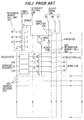
- the conventional memory device with current mirror type sense amplifiers comprises a reference memory cell unit 100, information memory cell units 200 of a matrix pattern, sense amplifiers 300 connected through a reference voltage line 13 to the reference memory cell unit 100 and through digit lines 16 to columns of the information memory cell units 200, and an address decoder units 400 connected through selection and word lines 17 and 18 to 20 to rows of the information memory cell units 200.
- the reference memory cell unit 100 comprises a selection NMOS transistor 1, reference NMOS transistors 2 and 3, and a reference NMOS transistor 4 of depletion type connected in serial by source-drain path, wherein the selection NMOS transistor 1 is connected in source-drain path to a source-drain path and a gate of a PMOS transistor 9 connected to a high voltage power supply 12, the selection and reference NMOS transistors 1, 2 and 3 are connected at gates to the high voltage power supply 12, and the depletion type NMOS transistor 4 is connected at a gate to ground.
- the information memory cell unit 200 comprises a selection NMOS transistor, information memory cell NMOS transistors 6 to 8, among which the NMOS transistor 7 is of a depletion type, connected in serial between a digit line 16 and ground by source-drain path, wherein the selection NMOS transistor 5 is connected at a gate to a selection line 17, and the information memory cell NMOS transistors 6 to 8 are connected at gates to word lines 18 to 20.
- the sense amplifier 300 comprises a PMOS transistor 10 connected in source-drain path to the high voltage power supply 12 and the digit line 16 and at a gate to the reference voltage line 13, and an inverter 11 connected at an input to a nodal point between the source-drain path of the PMOS transistor 10 and the digit line 16 and at an output to an output signal line 25 which is provided in parallel to other output signal lines 26, 27, ....
- the address decoder unit 400 comprises a selector 21 connected through the selection line 17 to a gate of the selection NMOS transistor 5, and gates of selection NMOS transistors of other memory cell units of the same row, and an address decoder having an output of three bits 22, 23 and 24 is connected through the word lines 18, 19 and 20 to gates of the memory cell NMOS transistors 18, 19 and 20, and gates of memory cell NMOS transistors of the other memory cell units of the same row.
- the selection and reference memory cell NMOS transistors 1 to 4 are turned on in the reference memory cell unit 100, so that the PMOS transistor 9 is turned on, when a potential of the selection NMOS transistor 1 is lowered at a drain to be a predetermined value.
- the drain of the selection NMOS transistor 1 is maintained to be an intermediate potential VR between potentials of the high voltage power supply 12 and ground, so that the reference voltage line 13 is also maintained to be the potential VR.
- selection and information memory cell NMOS transistors 5 to 8 are turned on.
- selection NMOS transistors connected to the digit line 16 are turned off in other rows, because selectors of address decoder units of the other rows supply the ground level potential to selection lines thereof.
- the PMOS transistor 10 is turned on based on the intermediate potential VR applied to the gate thereof.
- a potential of the digit line 16 is set to be a value between the high and ground potentials determined by a ratio of serial resistances of the PMOS transistor 10, the selection NMOS transistor 5, and the memory cell NMOS transistors 6 to 8, among which the NMOS transistor 7 is of the depletion type.
- This digit line potential is determined to be a low level by the inverter 11, so that a high level signal is obtained as a content of the memory cell unit 200 at the output signal line 25.
- the address decoder of the address decoder unit 400 supplies the three bit signals 22 to 24 of "1", "1" and "0" to the word lines 18 to 20, the memory cell NMOS transistor 20 is not turned on, although the remaining NMOS transistors are turned on, so that the digit line 16 is set to be at a high potential. Consequently, a low level signal is read from the memory cell unit 200 to be obtained at the output signal line 25.
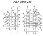
- Figs. 2A and 2B show the arrangement of information memory cell units provided on a chip of a semiconductor integrated circuit.
- the information memory cell units comprise selection NMOS transistors 48 and 52 having gates realized by an interconnection functioning as a selection line 37, information memory cell NMOs transistors 49 and 53 having gates realized by an interconnection functioning as a word line 40, information memory cell NMOS transistors 50 and 54 having gates realized by an interconnection functioning as a word line 43, and information memory cell NMOS transistors 51 and 55 having gates realized by an interconnection functioning as a word line 46.
- reference numerals 31 and 32 denote digit lines, 33 a connection point (through hole) between the drain diffusion layer 35 and the digit line 31, 34 a connection point (through hole) between the drain diffusion layer and the digit line 32, 35 and 36 drain diffusion layers of the NMOS transistors 48 and 52, 38 a source diffusion layer of the NMOS transistor 48 and a drain diffusion layer of the NMOS transistor 49, 39 a source diffusion layer of the NMOS transistor 52 and a drain diffusion layer of the NMOS transistor 53, 41 a source diffusion layer of the NMOS transistor 49 and a drain diffusion layer of the NMOS transistor 50, 42 a source diffusion layer of the NMOS transistor 53 and a drain diffusion layer of the NMOS transistor 54, 44 a source diffusion layer of the NMOS transistor 50 and a drain diffusion layer of the NMOS transistor 51, 45 a source diffusion layer of the NMOS transistor 54 and a drain diffusion layer of the NMOS transistor 56, and 47 source diffusion layers (ground potential) of the NMOS
- the unevenness of characteristics of the NMOS transistors resulting from the fabrication process can be small, because the NMOS transistors are addressed by the common word lines, and are fabricated with short distances on the chip.
- the current mirror type memory device comprises reference memory cell units 100, information memory cell units 200 arranged in matrix pattern, sense amplifiers 300 connected to columns of the information memory cell units 200, and address decoder units 400 connected to rows of the information memory cell units 200.
- the reference memory cell units 100 are arranged to correspond to the rows of the information memory cell units 200.
- Each of the reference memory cell units 100 comprises a selection NMOS transistor 1 and reference memory cell NMOS transistors 2 to 4 of a depletion type.
- the NMOS transistors 1 to 4 are connected in serial by source-drain path, wherein the selection NMOS transistor is connected at a drain to a reference voltage line 13 and at a gate to a selection line 17, the depletion type NMOS transistors 2 to 4 are connected at gates to word lines 18 to 20, respectively, and the depletion type NMOs transistor 4 is connected at a source to ground.
- a PMOS transistor 9 is connected at a source to a high voltage power supply 12, and at gate and drain to the reference voltage line 13.
- a selection NMOS transistor 5, and information memory cell NMOS transistors 6 to 8, among which the NMOS transistor 7 is of a depletion type, are connected in serial by source-drain path, wherein a drain of the selection NMOS transistor 5 is connected to a digit line 16 and a source of the information memory cell NMOs transistor 8 is connected to ground.
- Each of the sense amplifiers 300 comprises a PMOS transistor 10 connected at a source to the high voltage power supply 12, at a gate to the reference voltage line 13, and at a drain to the digit line 16, and an inverter 11 connected an input to the digit line 16 and at an output to an output signal line 25 provided in parallel to other output signal lines 26, 27, .
- Each of the address decoder units 400 comprises a selector 21 having a selection line 17 connected to gates of the selection NMOS transistors 1 and 5, and other selection NMOS transistors of the same row, and an address decoder of three bit outputs 22 to 24 connected to word lines 18 to 20, to which gates of the reference memory cell and information memory cell NMOS transistors 2 to 4 and 6 to 8 are connected, respectively.
- one column of the reference memory cell units 100 of the number equal to that of rows of the information memory cell units 200 are provided in the similar pattern that one column of the address decoder units 400 are provided to address one of the rows of the information memory cell units 200.
- one row of the sense amplifiers 300 of the number equal to that of columns of the information memory cell units 200 are provided to read information therefrom in parallel to the output signal lines 25, 26, 27, .
- a potential of the selection line 17 is set to be a high potential by the selector 21 of the address decoder unit 400, so that the selection NMOS transistor 1 of the reference memory cell unit 100 is turned on.
- the reference voltage line 13 is connected through the selection NMOS transistor 1 and the depletion type NMOs transistors 2 to 4 to ground, so that a potential of the reference voltage line 13 is set to be the intermediate potential VR, as described before.
- the information memory cell units 200 of the same row are connected to the digit line 16 and other digit lines in accordance with the turning-on of the selection NMOS transistor 17 and other selection NMOS transistors of the same row.
- information is read from the information memory cell units 200 of the same row, as described before.
- This invention may be applied to an ultraviolet ray erasing type programmable read only memory in which a potential of word lines is set to be higher than a high voltage of a power supply.
Landscapes
- Engineering & Computer Science (AREA)
- Microelectronics & Electronic Packaging (AREA)
- Read Only Memory (AREA)
- Static Random-Access Memory (AREA)
Claims (4)
- Dispositif de mémoire avec des amplificateurs de détection de type miroir de courant, comprenant :- une pluralité d'unités de cellules de mémoire d'information (200) disposées dans une configuration matricielle ayant un nombre prédéterminé de colonnes et un nombre prédéterminé de rangées, chacune desdites unités de cellules de mémoire d'information comprenant une cellule de sélection (5) et des cellules de mémoire d'information (6,7,8), dans lequel lesdites cellules de mémoire d'information sont des transistors (6,7,8) connectés en série et ladite cellule de sélection est un transistor (5) connecté en série avec lesdites cellules de mémoire d'information, des informations étant mémorisées dans au moins une desdites cellules de mémoire d'information;- une pluralité d'unités de décodage d'adresse (400), chacune comprenant un sélecteur (21) pour commander l'état passant et l'état bloqué de ladite cellule de sélection (5) et un décodeur d'adresse (22,23,24) pour accéder auxdites cellules de mémoire d'information (6,7,8), ledit sélecteur étant connecté dans chaque rangée à ladite cellule de sélection par une ligne de sélection (17), et ledit décodeur d'adresse étant connecté à des sorties dans ladite chaque rangée auxdites cellules de mémoire d'information (6,7,8) par des lignes de mot (18,19,20);- une pluralité d'amplificateurs de détection (300) connectés à des colonnes desdites unités de cellules de mémoire d'information par des lignes de bit (16), respectivement; et- une pluralité d'unités de cellules de mémoire de référence (100), chacune comprenant une cellule de sélection (1) et des cellules de mémoire de référence (2,3,4), et connectées à des rangées desdites unités de cellules de mémoire d'information, respectivement, de telle sorte que ladite cellule de sélection (1) est connectée dans ladite chaque rangée audit sélecteur (21) par ladite ligne de sélection (17) et lesdites cellules de mémoire de référence (2,3,4) sont connectées dans ladite chaque rangée auxdites sorties dudit décodeur d'adresse (22,23,24) par lesdites lignes de mot (18,19,20), de manière à ce qu'une desdites unités de cellules de mémoire de référence applique une tension de référence (VR) à une ligne de tension de référence (13) connectée auxdits amplificateurs de détection (300), lorsque ladite cellule de sélection (1) est sélectionnée dans ladite une desdites unités de cellules de mémoire de référence par ledit sélecteur (21) de ladite unité de décodage d'adresse, et dans lequel chaque unité de cellules de mémoire de référence (100) comprend une pile unique de transistors de cellules de mémoire de référence (2,3,4) de type à déplétion et d'un transistor de sélection (1) de type à enrichissement connectés en série.
- Dispositif de mémoire avec des amplificateurs de détection de type miroir de courant selon la revendication 1, dans lequel :- lesdits transistors sont des transistors NMOS, au moins un (7) desdits transistors NMOS compris dans lesdites cellules de mémoire d'information étant de type à déplétion; et- ladite cellule de sélection de référence (1) et lesdites cellules de mémoire de référence (2,3,4) sont des transistors NMOS dans ladite chacune desdites unités de cellules de mémoire de référence (100), lesdits transistors NMOS (2,3,4) compris dans lesdites cellules de mémoire de référence étant de type à déplétion.
- Dispositif de mémoire avec des amplificateurs de détection de type miroir de courant selon la revendication 1, dans lequel :- lesdits transistors sont des transistors NMOS, au moins un (7) desdits transistors NMOS compris dans lesdites cellules de mémoire d'information étant de type à déplétion, lesdits transistors étant connectés en série entre ladite ligne de bit (16) et la masse par un chemin source-drain, et par des grilles à ladite ligne de sélection (17) et auxdites lignes de mot (18,19,20), respectivement; et- chacune desdites unités de cellules de mémoire de référence (100) comprend un transistor NMOS de sélection de référence (1) et trois transistors NMOS de cellules de mémoire de référence (2,3,4) de type à déplétion connectés en série entre ladite ligne de tension de référence (13) et la masse par un chemin source-drain, et par des grilles à ladite ligne de sélection (17) et auxdites lignes de mot (18,19,20), respectivement.
- Dispositif de mémoire avec des amplificateurs de détection de type miroir de courant selon l'une quelconque des revendications précédentes, dans lequel :- lesdites unités de cellules de mémoire de référence (100) sont connectées auxdits amplificateurs de détection (300) par ladite ligne de tension de référence (13);- ladite ligne de tension de référence (13) est connectée à un drain et à une grille d'un premier transistor PMOS (9) connecté par une source à un bloc d'alimentation à haute tension (12); et- chacun desdits amplificateurs de détection (300) comprend un deuxième transistor PMOS (10), connecté par une grille à ladite ligne de tension de référence (13), par un drain à ladite ligne de bit (16) et par une source audit bloc d'alimentation à haute tension (12), et un inverseur (11) connecté par une entrée à ladite ligne de bit (16) connectée audit drain dudit deuxième transistor PMOS (10) et par une sortie à une ligne de signal de sortie (25).
Applications Claiming Priority (2)
| Application Number | Priority Date | Filing Date | Title |
|---|---|---|---|
| JP2327737A JPH04195900A (ja) | 1990-11-27 | 1990-11-27 | カレントミラー型センスアンプ |
| JP327737/90 | 1990-11-27 |
Publications (3)
| Publication Number | Publication Date |
|---|---|
| EP0488672A2 EP0488672A2 (fr) | 1992-06-03 |
| EP0488672A3 EP0488672A3 (en) | 1992-07-15 |
| EP0488672B1 true EP0488672B1 (fr) | 1997-04-09 |
Family
ID=18202422
Family Applications (1)
| Application Number | Title | Priority Date | Filing Date |
|---|---|---|---|
| EP91310916A Expired - Lifetime EP0488672B1 (fr) | 1990-11-27 | 1991-11-27 | Dispositif de mémoire avec des amplificateurs de détection de type courant à miroir |
Country Status (5)
| Country | Link |
|---|---|
| US (1) | US5297084A (fr) |
| EP (1) | EP0488672B1 (fr) |
| JP (1) | JPH04195900A (fr) |
| KR (1) | KR970010644B1 (fr) |
| DE (1) | DE69125576T2 (fr) |
Families Citing this family (6)
| Publication number | Priority date | Publication date | Assignee | Title |
|---|---|---|---|---|
| KR950013342B1 (ko) * | 1992-10-06 | 1995-11-02 | 삼성전자주식회사 | 반도체 메모리장치의 결함구제회로 |
| JP3204799B2 (ja) * | 1993-04-28 | 2001-09-04 | 株式会社東芝 | 半導体メモリ装置 |
| JP2591907B2 (ja) * | 1994-05-24 | 1997-03-19 | 日本電気アイシーマイコンシステム株式会社 | 読み出し専用半導体記憶装置のデコード回路 |
| US5621680A (en) * | 1996-04-01 | 1997-04-15 | Motorola, Inc. | Data storage element and method for reading data therefrom |
| FR2751778B1 (fr) * | 1996-07-23 | 1998-11-06 | Sgs Thomson Microelectronics | Memoire accessible en lecture seulement |
| JP2978813B2 (ja) * | 1997-02-27 | 1999-11-15 | 日本電気アイシーマイコンシステム株式会社 | 半導体記憶回路 |
Family Cites Families (7)
| Publication number | Priority date | Publication date | Assignee | Title |
|---|---|---|---|---|
| JPS6022436B2 (ja) * | 1978-01-27 | 1985-06-01 | 株式会社日立製作所 | ダイナミツク型rom |
| US4305139A (en) * | 1979-12-26 | 1981-12-08 | International Business Machines Corporation | State detection for storage cells |
| US4648074A (en) * | 1984-06-29 | 1987-03-03 | Rca Corporation | Reference circuit with semiconductor memory array |
| JPS6271098A (ja) * | 1985-09-25 | 1987-04-01 | Hitachi Ltd | 半導体記憶装置 |
| US4713797A (en) * | 1985-11-25 | 1987-12-15 | Motorola Inc. | Current mirror sense amplifier for a non-volatile memory |
| JPH0793033B2 (ja) * | 1989-08-24 | 1995-10-09 | 日本電気株式会社 | センスアンプ |
| US5132933A (en) * | 1990-12-21 | 1992-07-21 | Schreck John F | Bias circuitry for nonvolatile memory array |
-
1990
- 1990-11-27 JP JP2327737A patent/JPH04195900A/ja active Pending
-
1991
- 1991-11-26 US US07/798,646 patent/US5297084A/en not_active Expired - Lifetime
- 1991-11-27 DE DE69125576T patent/DE69125576T2/de not_active Expired - Fee Related
- 1991-11-27 EP EP91310916A patent/EP0488672B1/fr not_active Expired - Lifetime
- 1991-11-27 KR KR1019910021369A patent/KR970010644B1/ko not_active Expired - Fee Related
Also Published As
| Publication number | Publication date |
|---|---|
| EP0488672A2 (fr) | 1992-06-03 |
| DE69125576T2 (de) | 1997-08-07 |
| JPH04195900A (ja) | 1992-07-15 |
| KR920010615A (ko) | 1992-06-26 |
| EP0488672A3 (en) | 1992-07-15 |
| DE69125576D1 (de) | 1997-05-15 |
| US5297084A (en) | 1994-03-22 |
| KR970010644B1 (ko) | 1997-06-28 |
Similar Documents
| Publication | Publication Date | Title |
|---|---|---|
| US5594687A (en) | Completely complementary MOS memory cell with tunneling through the NMOS and PMOS transistors during program and erase | |
| US5917753A (en) | Sensing circuitry for reading and verifying the contents of electrically programmable/erasable non-volatile memory cells | |
| US6577530B2 (en) | Semiconductor memory device having memory cells each capable of storing three or more values | |
| US6600671B2 (en) | Reduced area sense amplifier isolation layout in a dynamic RAM architecture | |
| US5282175A (en) | Semiconductor memory device of divided word line | |
| US4455629A (en) | Complementary metal-insulated semiconductor memory decoder | |
| EP0055594B1 (fr) | Dispositif de mémoire non-volatile à semi-conducteur programmable électriquement | |
| US5274597A (en) | Semiconductor memory device capable of driving divided word lines at high speed | |
| GB2168213A (en) | A read only semiconductor memory | |
| EP0044978B1 (fr) | Mémoire à lecture seulement | |
| JP2573380B2 (ja) | 不揮発性半導体メモリ | |
| US5387827A (en) | Semiconductor integrated circuit having logic gates | |
| US5687125A (en) | Semiconductor memory device having redundancy memory cells incorporated into sub memory cell blocks | |
| EP0040045A1 (fr) | Dispositif de mémoire morte | |
| US4924438A (en) | Non-volatile semiconductor memory including a high voltage switching circuit | |
| EP0488672B1 (fr) | Dispositif de mémoire avec des amplificateurs de détection de type courant à miroir | |
| EP0503524B1 (fr) | Dispositif de mémoire à semi-conducteurs | |
| US7345945B2 (en) | Line driver circuit for a semiconductor memory device | |
| US4376987A (en) | Threshold referenced MNOS sense amplifier | |
| EP0365720B1 (fr) | Mémoire à semi-conducteurs programmable | |
| US4760562A (en) | MOS static memory circuit | |
| US5359555A (en) | Column selector circuit for shared column CMOS EPROM | |
| US5691944A (en) | Non-volatile semiconductor memory device | |
| US4628250A (en) | Power conserving CMOS reference voltage source | |
| US5198998A (en) | Erasable programmable read only memory |
Legal Events
| Date | Code | Title | Description |
|---|---|---|---|
| PUAI | Public reference made under article 153(3) epc to a published international application that has entered the european phase |
Free format text: ORIGINAL CODE: 0009012 |
|
| PUAL | Search report despatched |
Free format text: ORIGINAL CODE: 0009013 |
|
| 17P | Request for examination filed |
Effective date: 19911209 |
|
| AK | Designated contracting states |
Kind code of ref document: A2 Designated state(s): DE FR GB |
|
| AK | Designated contracting states |
Kind code of ref document: A3 Designated state(s): DE FR GB |
|
| 17Q | First examination report despatched |
Effective date: 19950808 |
|
| GRAG | Despatch of communication of intention to grant |
Free format text: ORIGINAL CODE: EPIDOS AGRA |
|
| GRAH | Despatch of communication of intention to grant a patent |
Free format text: ORIGINAL CODE: EPIDOS IGRA |
|
| GRAH | Despatch of communication of intention to grant a patent |
Free format text: ORIGINAL CODE: EPIDOS IGRA |
|
| GRAA | (expected) grant |
Free format text: ORIGINAL CODE: 0009210 |
|
| AK | Designated contracting states |
Kind code of ref document: B1 Designated state(s): DE FR GB |
|
| REF | Corresponds to: |
Ref document number: 69125576 Country of ref document: DE Date of ref document: 19970515 |
|
| ET | Fr: translation filed | ||
| PLBE | No opposition filed within time limit |
Free format text: ORIGINAL CODE: 0009261 |
|
| 26N | No opposition filed | ||
| REG | Reference to a national code |
Ref country code: GB Ref legal event code: IF02 |
|
| REG | Reference to a national code |
Ref country code: GB Ref legal event code: 732E |
|
| REG | Reference to a national code |
Ref country code: FR Ref legal event code: TP |
|
| PGFP | Annual fee paid to national office [announced via postgrant information from national office to epo] |
Ref country code: FR Payment date: 20041109 Year of fee payment: 14 |
|
| PGFP | Annual fee paid to national office [announced via postgrant information from national office to epo] |
Ref country code: GB Payment date: 20041124 Year of fee payment: 14 |
|
| PGFP | Annual fee paid to national office [announced via postgrant information from national office to epo] |
Ref country code: DE Payment date: 20041125 Year of fee payment: 14 |
|
| PG25 | Lapsed in a contracting state [announced via postgrant information from national office to epo] |
Ref country code: GB Free format text: LAPSE BECAUSE OF NON-PAYMENT OF DUE FEES Effective date: 20051127 |
|
| PG25 | Lapsed in a contracting state [announced via postgrant information from national office to epo] |
Ref country code: DE Free format text: LAPSE BECAUSE OF NON-PAYMENT OF DUE FEES Effective date: 20060601 |
|
| GBPC | Gb: european patent ceased through non-payment of renewal fee |
Effective date: 20051127 |
|
| PG25 | Lapsed in a contracting state [announced via postgrant information from national office to epo] |
Ref country code: FR Free format text: LAPSE BECAUSE OF NON-PAYMENT OF DUE FEES Effective date: 20060731 |
|
| REG | Reference to a national code |
Ref country code: FR Ref legal event code: ST Effective date: 20060731 |