EP0488719A2 - Système et méthode pour détecter des décharges partielles d'interrupteurs à gaz - Google Patents
Système et méthode pour détecter des décharges partielles d'interrupteurs à gaz Download PDFInfo
- Publication number
- EP0488719A2 EP0488719A2 EP91310997A EP91310997A EP0488719A2 EP 0488719 A2 EP0488719 A2 EP 0488719A2 EP 91310997 A EP91310997 A EP 91310997A EP 91310997 A EP91310997 A EP 91310997A EP 0488719 A2 EP0488719 A2 EP 0488719A2
- Authority
- EP
- European Patent Office
- Prior art keywords
- signal
- frequency
- partial discharge
- voltage
- converting
- Prior art date
- Legal status (The legal status is an assumption and is not a legal conclusion. Google has not performed a legal analysis and makes no representation as to the accuracy of the status listed.)
- Granted
Links
Images


Classifications
-
- G—PHYSICS
- G01—MEASURING; TESTING
- G01R—MEASURING ELECTRIC VARIABLES; MEASURING MAGNETIC VARIABLES
- G01R31/00—Arrangements for testing electric properties; Arrangements for locating electric faults; Arrangements for electrical testing characterised by what is being tested not provided for elsewhere
- G01R31/12—Testing dielectric strength or breakdown voltage ; Testing or monitoring effectiveness or level of insulation, e.g. of a cable or of an apparatus, for example using partial discharge measurements; Electrostatic testing
- G01R31/1227—Testing dielectric strength or breakdown voltage ; Testing or monitoring effectiveness or level of insulation, e.g. of a cable or of an apparatus, for example using partial discharge measurements; Electrostatic testing of components, parts or materials
- G01R31/1254—Testing dielectric strength or breakdown voltage ; Testing or monitoring effectiveness or level of insulation, e.g. of a cable or of an apparatus, for example using partial discharge measurements; Electrostatic testing of components, parts or materials of gas-insulated power appliances or vacuum gaps
-
- G—PHYSICS
- G01—MEASURING; TESTING
- G01R—MEASURING ELECTRIC VARIABLES; MEASURING MAGNETIC VARIABLES
- G01R31/00—Arrangements for testing electric properties; Arrangements for locating electric faults; Arrangements for electrical testing characterised by what is being tested not provided for elsewhere
- G01R31/327—Testing of circuit interrupters, switches or circuit-breakers
- G01R31/3271—Testing of circuit interrupters, switches or circuit-breakers of high voltage or medium voltage devices
- G01R31/3275—Fault detection or status indication
-
- H—ELECTRICITY
- H01—ELECTRIC ELEMENTS
- H01H—ELECTRIC SWITCHES; RELAYS; SELECTORS; EMERGENCY PROTECTIVE DEVICES
- H01H33/00—High-tension or heavy-current switches with arc-extinguishing or arc-preventing means
- H01H33/02—Details
- H01H33/26—Means for detecting the presence of an arc or other discharge
Definitions
- the present invention relates to a partial discharge detecting system for detecting partial discharge generated in the interior of gas-insulated switchgear.
- gas-insulated switchgear has become common, wherein a disconnector or circuit breaker, etc., is accommodated in a sealed enclosure filled with SF6 gas, which has excellent insulating and arc-extinguishing properties.
- SF6 gas which has excellent insulating and arc-extinguishing properties.
- a vital part of such gas-insulated switchgear is means which is used to detect any abnormality occurring in the sealed enclosure.
- One such detecting means is a partial discharge detecting system that detects partial discharge occurring in the interior of the gas-insulated switchgear.
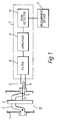
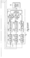
- FIG. 1 of the accompanying drawings shows an example of a conventional partial discharge detecting system.
- a metal enclosure 1 of gas-insulated switchgear 12 is grounded to earth and filled with the insulating gas SF6.
- the enclosure is electrically divided by a bell-shaped insulation spacer 2 and coupled in the longitudinal direction.
- Metal enclosure 1 accommodates a disconnector or circuit breaker (not shown) constituting the gas-insulated switchgear.
- Figure 1 shows part of the region where a conductor 3 supported by the insulation spacer 2 is accommodated. This conductor 3 connects a transformer with the disconnector or circuit breaker.
- a ring-shaped electrode 4 for checking the voltage is arranged in insulation spacer 2.
- a floating capacitance C1 is, therefore, present between the conductor 3 and electrode 4 and a floating capacitance C2 is present between metal enclosure 1 and electrode 4.
- a partial discharge detector 7 is provided with a filter 8, connected to electrode 4 and metal enclosure 1 by means of leads 5 and 6, respectively, that extracts the frequency of the partial discharge, an amplifier circuit 9 that amplifies the output signal of filter 8, and a peak detector circuit 10 that detects the peak value of the output signal of the amplifier circuit 9.
- floating capacitances C1 and C2 constitute a voltage-dividing circuit, so a divided voltage is generated at the two terminals of floating capacitance C2. A high-frequency component created by the partial discharge in metal enclosure 1 is superimposed on this divided voltage.
- the high-frequency component contained in the divided voltage is, therefore, extracted by filter 8 and its peak value is detected by peak detector circuit 10 through amplifier circuit 9. This detected peak value is output to a measurement device 11.
- Figure 2 shows the causes of partial discharge generated in metal enclosure 1 and the pattern of the resulting partial discharge pulse.
- Reason for partial discharge 1 may be further subdivided into case (1 - 1), in which discharge is produced due to the presence of bubbles or voids in the insulator in metal enclosure 1, and case (1 - 2), in which discharge is produced due to the formation of a gap at the contact surface of the insulator and conductor.
- Partial discharge 2 is produced when a part of the insulator projects into the region in metal enclosure 1 that is filled with insulating gas (sharp edge).
- Partial discharge 3 is produced when part of the metal projects into the region in metal enclosure 1 that is filled with insulating gas (loose metal particles).
- Partial discharge 4 is produced when there is poor contact at locations where one conductor is in contact with another conductor in metal enclosure 1.
- a system for detecting partial discharge generated in the interior of gas-insulated switchgear comprises high-frequency detection means for detecting a high-frequency component of a voltage applied to said gas-insulated switchgear; fundamental wave detection means for detecting the fundamental wave component of the voltage applied to said gas-insulated switchgear; voltage starting-point setting means for detecting a zero-crossing point of the fundamental wave component obtained by said fundamental wave detection means, and setting a starting point based upon said zero-crossing point; detected signal processing means for performing signal processing on an output signal of said high-frequency detection means and on an output signal of said voltage starting-point setting means, and outputting respective first and second optical signals corresponding to said output signals; and partial discharge decision means for converting said first and second optical signals into respective first and second pulse signals and ascertaining an occurrence of partial discharge and a reason for the occurrence of partial discharge, based on said first and second pulse signals.
- the invention produces the first pulse signal representing the high-frequency compoment of the fundamental wave and can determine the presence of, and reason for, the partial discharge as the positions of the partial discharge pulses relative to the fundamental wave depend on the cause of the partial discharge.
- a system for detecting partial discharge generated in the interior of gas-insulated switchgear comprises first high-frequency detection means, provided at a bushing of the gas-insulated switchgear, for detecting a first high-frequency component superimposed on the voltage applied to the conductor of said gas-insulated switchgear, caused by external noise entering the gas-insulated switchgear, second high-frequency detection means, provided at a central location of the gas-insulated switchgear, for detecting a second high-frequency component superimposed on the voltage applied to the conductor of said gas-insulated switchgear, caused by partial discharge in said interior of the gas-insulated suitchgear, fundamental wave detection means for detecting a fundamental wave component of the voltage applied to the conductor of gas-insulated switchgear, voltage starting-point setting means for detecting a zero-crossing point of the fundamental wave component obtained by the fundamental wave detection means, and setting a starting point based upon for said zero-crossing point, detected signal processing means for performing signal processing on a first output signal of the first high-
- a first aspect of the method for detecting partial discharge generated in the interior of a gas-insulated switchgear includes the steps of detecting a high-frequency component of a voltage applied to a conductor of the gas-insulated switchgear, detecting a fundamental wave component of the voltage applied to the conductor of the gas-insulated switchgear, determining whether the partial discharge has occurred, and a reason for the partial discharge, based upon a relationship between the high-frequency component of and the fundamental wave component of the voltage applied to the conductor of the gas-insulated switchgear.
- a second aspect of the method for detecting partial discharge generated in the interior of a gas-insulated switchgear includes the steps of detecting a first high-frequency component of a voltage applied to a conductor of said gas-insulated switchgear due to noise superimposed on said voltage, detecting a second high-frequency component of the voltage applied to the conductor of the gas-insulated switchgear due to the partial discharge in the interior of the gas-insulated switchgear, detecting a fundamental wave component of the voltage applied to the conductor of the gas-insulated switchgear, determining whether the partial discharge has occurred, and a reason for the partial discharge, based upon a relationship between the first and second high-frequency components and the fundamental wave component of the voltage applied to said conductor of said gas-insulated switchgear.
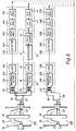
- FIG. 3 shows a first embodiment of a partial discharge detecting system of a gas-insulated switchgear according to this Invention.
- Gas-insulated switchgear 12 is the same as that shown in Fig. 1.
- a voltage division circuit for the applied voltage is formed by floating capacitances C1and C2.
- the high-frequency component created by partial discharge occurring within metal enclosure 1 is superimposed on this divided voltage.
- High-frequency detecting device 22 of partial discharge detecting system 21 detects the high-frequency component contained in divided voltage V C2 between leads 5 and 6. It comprises a transformer 311 that transforms divided voltage V C2, a band-pass filter 32 that extracts the high-frequency component caused by partial discharge in the output signal of transformer 311, and an amplifier 33 that amplifies the output signal of band-pass filter 32.
- a fundamental wave detecting device 23 which detects the fundamental wave component of divided voltage V C2 i.e., the mains frequency component. It comprises a transformer 312 that transforms divided voltage V C2 , a band-pass filter 39 that extracts the fundamental wave component of the output signal of transformer 312, and an amplifier 40 that amplifies the output signal of band-pass filter 39.
- the fundamental wave component of divided voltage V C2 extracted by fundamental wave detecting means 23 is input to a setting device 24 of the starting point for the voltage.
- Voltage starting point setting device 24 detects the zero-crossing point of the fundamental wave component of dividing voltage V C2 and outputs this as the starting point for the voltage, in the form of a pulse signal.
- This voltage starting point setting device 24 consists of a comparator 41 that detects the zero-crossing point of the output signal of fundamental wave detecting device 23 and outputs a pulse signal, and a pulse shaping circuit 42 that shapes the waveform of the pulse signal of comparator 41.
- the output signal of high-frequency detecting device 22 and the output signal of voltage starting point setting device 24 are input to a detected signal processing device 25.
- Detected signal processing device 25 carries out signal processing on the high-frequency component contained in dividing voltage V C2 detected by high-frequency detecting device 22 and on the pulse signal indicating the starting point for the voltage which is obtained by voltage starting point setting device 24 to produce a signal that is suitable for optical transmission to a partial discharge ascertaining device 26.
- the high-frequency component contained in divided voltage V C2 detected by high-frequency detecting device 22 is detected by a detector circuit 34 of detected signal processing device 25 and the output signal of detector circuit 34 is converted to a fixed pulse width by a peak hold circuit 35.
- the output signal of peak hold circuit 34 is then frequency-modulated by a V/F converter circuit. This frequency-modulated signal is then converted to an optical signal by an E/O converter 37 and input to partial discharge ascertaining device 26 through an optical fiber 281.
- the pulse signal from voltage starting point setting device 24 indicating the starting point for the voltage is input to a V/F converter 43 of detected signal processing device 25, where it is frequency-modulated.
- This frequency-modulated signal is then converted to an optical signal by an E/O converter 44, and input to partial discharge ascertaining device 26 through an optical fiber 282.
- Partial discharge ascertaining device 26 converts the optical signals that are input through optical fibers 281 and 282 into pulse signals P3 and P1, respectively, (see Fig. 4). Based on pulse signal P3 indicating the magnitude of the high-frequency component of dividing voltage V C2 and pulse signal P1 indicating the starting point for the voltage of dividing voltage V C2 , partial discharge ascertaining device 26 ascertains whether partial discharge is taking place, and the reason or reasons for the occurrence of such partial discharge.
- the optical signal indicating the magnitude of the high-frequency component of the dividing voltage V C2 that is input from detected signal processing device 25 is converted to pulse signal P3 indicating the magnitude of the high-frequency component of dividing voltage V C2 by means of an O/E converter 47, F/V converter 48, amplifier 49, and integrating circuit 50.
- the optical signal indicating the starting point for the voltage of dividing voltage V C2 that is input from detected signal processing device 25 is converted to pulse signal P1 indicating the starting point for the voltage of dividing voltage V C2 by means of an O/E converter 53, F/V converter 54, amplifier 55, and waveform shaping circuit 56.
- Pulse signal P1 indicating the starting point for the voltage is input to a computing element 29.
- Computing element 29 can be implemented using a CPU, a microprocessor or a computer, for example.
- computing element 29 Based on this pulse signal P1, computing element 29 outputs an instrumentation timing pulse signal P2 to an A/D converter 51.
- A/D converter 51 introduces the pulse signal P4 indicating the high frequency component into computing element 29 only during the period when instrumentation timing pulse signal P2 is being input.
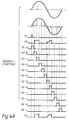
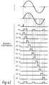
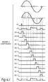
- Figs. 4A-4J are diagrams given in explanation of the operation of partial discharge detecting system partial discharge detecting system 21 of this invention. How, fundamental wave component V0 of dividing voltage V C2 contains a high frequency component V1. High frequency component V1 contained in dividing voltage V C2 is detected by high-frequency detecting device 22 and the detected high frequency component V1 is subjected to signal processing by detected signal processing device 25 to produce an optical signal which is optically transmitted to partial discharge ascertaining device 26.
- Fundamental wave component V0 of dividing voltage V C2 is detected by fundamental wave detecting device 23.
- Voltage starting point setting device 24 then converts the zero-crossing point of fundamental wave component V0 into a pulse signal constituting the starting point for the voltage. This is then subjected to signal processing by detected signal processing device 25 to produce an optical signal which is optically transmitted to partial discharge ascertaining device 26.
- Partial discharge ascertaining device 26 finds the high Frequency component V1 of dividing voltage V C2 as pulse signal P3 and fundamental wave component V0 of dividing voltage V C2 as pulse signal P 1.
- Computing element 29 of detected signal processing means 25 outputs instrumentation timing pulse signal P2 to A/D converter 51 based on pulse signal P1 indicating the starting point for the voltage.
- Instrumentation timing pulse signal P2 that is output by computing element 29 is a command signal, with reference to the starting point for the voltage, for introduction of pulse signal P4 indicating the magnitude of the high-frequency component to computing element 29.
- signal P4 is a digital signal to be input to computing element 29 in a form element 29 is able to process.
- the signal P4 in Figs. 4A-4J is shown for convenience of explanation and does not represent the actual shape of the signal sent to element 29. The reason for partial discharge as indicated in Fig. 2 can therefore be determined.
- timing pulse signal P2 which is a series of pulses P2-A to P2-L successively during the measurement time cycle period. While timing pulse signal P2 is shown as consisting of twelve pulses P2-A to P2-L, it is understand that this is given by way of example only and the actual number of pulses can be varied based upon the requirements of the partial discharge detecting system and the gas-insulated switchgear.
- Fig. 4A corresponds to a partial discharge due to a vacancy or bubble corresponding to reason 1-1 in the starting discharge condition as shown in Fig. 2.
- the signals P 2-A to P 2-L are received by A/D converter 51 converts the partial discharge pulse P3 to a digital signal which is input to computing element 29.
- Computing element 29 receives the digital signal P4 from A/D converter 51 and stores signal P4 in a memory section thereof. Computing element 29 then compares the stored signal P4 with other patterns stored beforehand and determines whether a partial discharge has occurred based upon the signal P4. If it is determined that a partial discharge has occurred, that is, the signal P4 corresponds to one of the known reasons for partial discharge, such as shown in Fig. 2, computing element 29 outputs a signal to an external display device and alarm 60 which displays the results of the partial discharge determination and produces an alarm. As is apparent from Fig. 4A, the signal P4 provides both pulse magnitude and pulse phase information relative to the fundamental wave which allows the determination of whether a partial discharge has occurred.
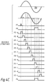
- figs. 4B-4J illustrate the determination of partial discharges corresponding to reasons 1-2, 2, 3 and 4 of the starting discharge condition and to reasons 1-1, 1-2, 2, 3 and 4 of the continuing discharge condition, respectively.
- computing element 29 is the same in each case, a detailed explanation of each Figure will be omitted for brevity.
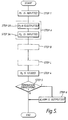
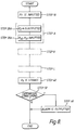
- Fig. 5 is flow diagram given an explanation of the operation of the first embodiment shown in Fig. 3.
- pulse signal P1 is inputted to computing element 29, which triggers the output of timing pulse signal P2.
- step A which consists of steps 2A and 3A
- pulse P2-A is outputted to A/D converter 51 and the portion of pulse signal P4 occurring during the duration of pulse P2-A is inputted to computing element 29.
- steps B-L The same procedure as in step A is repeated in steps B-L such that all of the pulses of timing pulse signal P2 are output to A/D converter 51 which converts pulse signal P3 into digital signal P4 , and the corresponding portions of digital signal P4 are input to computing element 29.
- signal P4 is stored in a memory section of computing element 29.
- Computing element 29 compares the stored digital signal P4 with other stored known patterns which correspond to the partial discharge pattern shown in Fig. 2 (step 5). If the digital signal P4 corresponds to one of the patterns, an alarm signal is generated and recorded in step 6. If the digital signal P4 does not correspond to one of the partial discharge patterns, then the measurement cycle ends.
- the signal of specific frequency corresponding to partial discharge that is isolated by band-pass filter 32 often contains noise, which gives rise to measurement error. This noise cannot be removed by the conventional method of simply converting to a fixed pulse signal using a peak hold circuit or the like.
- the first embodiment according to the invention only pulse signals P3 of specific frequency that are generated while instrumentation timing pulse signal P2 is being output are subjected to A/D conversion and measured. Such a pulse of specified frequency is therefore present at a phase position, with respect to the phase of the main circuit voltage, at which partial discharge pulses are most likely to be generated, i.e., a phase position at which such a pulse is unlikely to be the result of noise.
- timing pulse P2 can be output in the range where it is anticipated that partial discharge may occur.
- the cause of partial discharge can be ascertained from the pattern of occurrence by measuring whether there are any pulses of specified frequency in this range.
- a pulse resolution of about 1/100 of the period of the mains frequency is sufficient in order to measure partial discharge pulses in relation to the phase of the mains frequency voltage.
- the partial discharge pulses are subjected to peak-holding or integration within a time width on this order, forming pulse signals for optical transmission. These formed pulse signals are then V/F converted, then E/O converted, and transmitted optically to partial discharge ascertaining device 26 in a signal condition close to a digital signal. It is thereby possible to eliminate the effect of attenuation due to the length of the optical fiber cable or the effect of fluctuation in the amount of such attenuation due to the optical connector units.
- the time required for in situ adjustment of individual sensors can thereby be reduced, and unstable measurement conditions resulting from the amount of attenuation changing every time an optical connector is added or removed can be greatly reduced.
- Fig. 6 is a block diagram showing a second embodiment of the invention. This embodiment represents a further improvement over the first embodiment shown in Fig. 3.
- errors can still be caused by external noise present having a frequency that is being measured entering gas-insulated switchgear 21 while instrumentation timing pulse signal P2 is being output.
- the ingress of such external noise is infrequent and sporadic, it does present an obstacle to raising accuracy.
- the second embodiment is adapted to eliminate causes of error due to such external noise.
- the frequency of partial discharge pulses occurring in gas-insulated switchgears is generally some tens of MHz.
- partial discharges caused by external noise entering the gas-insulated switchgear through parts such as the bushing of the gas-insulated switchgear are below some 100 KHz, sometimes overlaid with high-frequency components of some tens of MHz or more.
- high-frequency components below some 100 KHz cannot be detected within the gas-insulated switchgear, and can only be detected in the vicinity of the bushing.
- the gas-insulated switchgear can be regarded as a distributed-constant circuit. Such high-frequency components are therefore propagated through the switchgear with little attenuation. Accordingly, in the second embodiment, arrangements are made whereby, if external noise enters the gas-insulated switchgear and a partial discharge is generated due to high-frequency components of some tens of MHz superimposed on this external noise, this can be identified as not representing partial discharge originating from a cause to be found within the gas-insulated switchgear itself.
- Respective high-frequency detection devices 22A and 22B are provided that detect high-frequency components in two different locations within the same gas-insulated switchgear.
- FIG. 5 shows two gas-insulated switchgears 12A and 12B, it is understood that switchgears 12A and 12B are provided for convenience of explanation only, and that switchgears 12A and 12B are two portions of a single gas-insulated switchgear 12 having two bushing parts 12A and 12B.
- first high-frequency detection device 22A is provided on bushing part 12A of gas-insulated switchgear 12 having a detection frequency set to under some 100 kHz. This can be used to decide whether any external noise has entered.
- Second high-frequency detection device 22B positioned in the middle of gas-insulated switchgear 12 having a detection frequency set to over some tens of MHz. This can be used to decide whether partial discharge has occurred within gas-insulated switchgear 12.
- First detected signal processing device 25A that performs signal processing of the output signal of first high-frequency detection device 22A, fundamental wave detecting device 23, and voltage starting point setting device 24 are the same as in the first embodiment shown in Fig. 3.
- Second detected signal processing device 25B that performs signal processing of the output signal of second high-frequency detection device 22B is the same as first high-frequency detection device 25A except that it does not have units 43 and 44 that perform signal processing on the signal from voltage starting point setting device 24.
- partial discharge ascertaining device 26 is the same as that of Fig. 3 except that units 47B, 48B, 49B and 50B that perform signal processing on the signals obtained through second high-frequency detection device 22B and second detected signal processing device 25B are added to partial discharge ascertaining device 26 of Fig. 3.
- First high-frequency detection device 22A detects external noise that is generated at bushings in the same bus or overhead line.
- the detection frequency of second high-frequency detection device 22B is higher than that of first high-frequency detection device 22A, so, because of the difference in propagation characteristics described above, partial discharge pulses generated in the interior at central position 12B of gas-insulated switchgear 12 and high-frequency components superimposed on external noise are detected.
- pulse signal P30 indicating the external noise and pulse signal P31 indicating partial discharge
- pulse signal P31 indicating partial discharge
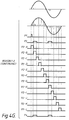
- FIG. 7 there is shown a diagram similar to Fig. 4A given an explanation of the operation of the first embodiment, but pulse signals of pulse timing signal P2 wave been omitted for brevity.
- Signal P 22A illustrates the fundamental wave having external noise detected by first high-frequency detecting device 22A.
- Units 47A, 48A, 49A, 50A produce pulse signal P30 which is input to A/D convorter 51A. It is evident that signal P30 provides both magnitude and phase information in relation to the fundamental wave of the noise detected by first high-frequency noise detecting device 22A.
- Second high-frequency detection device 22B connected to bushing part 12B detects the pulse signals on the fundamental wave which corresponds to signal P 22B .
- second detected signal processing device 25B and units 47B, 48B, 49B and 50B of partial discharge ascertaining device 26 produce signal P31 which provides magnitude and phase information of the pulse signals detected by second high-frequency detection device 22B.
- Signal P31 is input to A/D converter 51B in response to signal P2 output from computing element 74.
- step 10 signal P1 is inputted to computing device 74.
- computing element 74 Upon receiving signal P1, computing element 74 outputs pulse timing signal P2-A during step 20A of Step A.
- step 30A signals P30 and P31 are converted by A/O converters 51A and 51B, respectively, into digital signals P40 and P41, which are inputted to computing element 74.
- pulse signals P40 and P41 which correspond to the digitized values of pulse signals P30 and P31 are input to computing element 74 in response to pulse signals P2-B to P2-L.
- the operation of the second embodiment is similar to that of the first embodiment up to this point.
- Computing element 74 compares the input signals P40 and P41 and cancels the partial discharge pulses of signal P41 which are detected at the same time as the noise pulses of signal P40 to produce signal P50 which is stored in computing elements 74 and compared to patterns in the same manner of the first embodiment (step 40). If the signal P50 corresponds to one of the known discharge patterns (such as those shown in Fig. 2), the result is displayed and an alarm signal is generated using display device and alarm 60. On the other hand, if the signal P50 does not correspond to one of the patterns, the measuring cycle ends.
- computing element 74 Based on pulse signal P1 indicating the starting point for the voltage, computing element 74 outputs instrumentation timing pulse signal P2 to A/D converters 51A and 51B respectively.
- pulse signals P40 and P41 are input to computing element 74 practically simultaneously.
- signals P40, P41 and P50 are shown for convenience of explanation and do not represent the actual shape of the digital signal input to computing element 74. Any pulse signal P41 which is input into computing element 74 is cancelled while pulse signal P40 is also present at computing element 74.
- a partial discharge detection signal can be measured at the phase of the fundamental waveform of the voltage that has, for example, the highest probability of corresponding to a cause on partial discharge.
- the probability of mistaking noise for a partial discharge signal is therefore greatly reduced, making it possible to measure partial discharge accurately and with high reliability.
- phase analysis of partial discharge with respect to the fundamental waveform of the voltage becomes possible, and by collating the measured values and measured phase with said correlative relationship, the causes of occurrence of partial discharge can be elucidated.
Landscapes
- Physics & Mathematics (AREA)
- General Physics & Mathematics (AREA)
- Testing Relating To Insulation (AREA)
- Gas-Insulated Switchgears (AREA)
Applications Claiming Priority (3)
| Application Number | Priority Date | Filing Date | Title |
|---|---|---|---|
| JP336733/90 | 1990-11-30 | ||
| JP33673390 | 1990-11-30 | ||
| JP2336733A JPH04204270A (ja) | 1990-11-30 | 1990-11-30 | ガス絶縁開閉装置の部分放電検出装置 |
Publications (4)
| Publication Number | Publication Date |
|---|---|
| EP0488719A2 true EP0488719A2 (fr) | 1992-06-03 |
| EP0488719A3 EP0488719A3 (en) | 1992-11-04 |
| EP0488719B1 EP0488719B1 (fr) | 1998-01-14 |
| EP0488719B2 EP0488719B2 (fr) | 2001-04-18 |
Family
ID=18302217
Family Applications (1)
| Application Number | Title | Priority Date | Filing Date |
|---|---|---|---|
| EP91310997A Expired - Lifetime EP0488719B2 (fr) | 1990-11-30 | 1991-11-28 | Système et méthode pour détecter des décharges partielles d'interrupteurs à gaz |
Country Status (5)
| Country | Link |
|---|---|
| US (1) | US5200737A (fr) |
| EP (1) | EP0488719B2 (fr) |
| JP (1) | JPH04204270A (fr) |
| KR (1) | KR960004555B1 (fr) |
| DE (1) | DE69128698T3 (fr) |
Cited By (15)
| Publication number | Priority date | Publication date | Assignee | Title |
|---|---|---|---|---|
| EP0621489A3 (fr) * | 1993-03-24 | 1995-04-12 | Merlin Gerin | Dispositif de détection des décharges partielles pour l'appareillage électrique à haute tension. |
| FR2721408A1 (fr) * | 1994-06-20 | 1995-12-22 | Schneider Electric Sa | Dispositif de détection de décharges électriques pour appareillage électrique. |
| US5590012A (en) * | 1995-03-30 | 1996-12-31 | Siemens Energy & Automation, Inc. | Electric arc detector sensor circuit |
| WO1997007411A1 (fr) * | 1995-08-15 | 1997-02-27 | Siemens Aktiengesellschaft | Systeme pour mesurer des interferences electriques dans une installation de distribution electrique h.t. |
| WO1999006847A1 (fr) * | 1997-07-31 | 1999-02-11 | Siemens Aktiengesellschaft | Dispositif pour mesurer des decharges partielles dans des installations haute tension isolees au gaz |
| FR2783348A1 (fr) * | 1998-09-15 | 2000-03-17 | Alstom Technology | Methode de discrimination entre un arc interne et un arc de coupure dans un disjoncteur de moyenne ou de haute tension |
| FR2801981A1 (fr) * | 1999-12-07 | 2001-06-08 | Square D Co | Systeme et procede de simulation de panne par mise a la masse en presence d'un arc |
| GB2400246A (en) * | 2003-03-19 | 2004-10-06 | Diagnostic Monitoring Systems | Monitoring partial discharge events in gas insulated substations |
| EP1566646A1 (fr) * | 2004-02-20 | 2005-08-24 | Hitachi, Ltd. | Procédé et Dispositif pour mesurer des décharges partielles |
| GB2437315A (en) * | 2006-04-21 | 2007-10-24 | Mitsubishi Electric Corp | Diagnostic signal processor |
| WO2010036469A3 (fr) * | 2008-09-24 | 2010-08-19 | Siemens Energy, Inc. | Coupleur resistant aux decharges partielles pour application a des barres de bus d'alternateur haute tension |
| EP2290385A1 (fr) * | 2009-08-25 | 2011-03-02 | ABB Technology AG | Système de surveillance pour transformateurs de puissance et procédé de surveillance |
| WO2013139131A1 (fr) * | 2012-03-20 | 2013-09-26 | 上海市电力公司 | Dispositif d'amplification utilisé pour un système de surveillance en ligne de condensateur de décharge partielle |
| EP2343563A4 (fr) * | 2008-07-14 | 2014-07-09 | Power System Diagnosis Tech Inc | Dispositif servant à supprimer le bruit de décharge partielle d'une installation électrique et dispositif servant à détecter une zone générée par une décharge partielle |
| EP2542903A4 (fr) * | 2010-03-05 | 2015-03-11 | Ambient Corp | Evaluation des courants de bruit et des surintensités sur une ligne électrique |
Families Citing this family (27)
| Publication number | Priority date | Publication date | Assignee | Title |
|---|---|---|---|---|
| EP0491554B1 (fr) * | 1990-12-17 | 1996-05-22 | Patented Devices (Proprietary) Limited | Surveillance de décharges partielles |
| US5256977A (en) * | 1991-11-22 | 1993-10-26 | Axis Usa, Inc. | High frequency surge tester methods and apparatus |
| GB2270217B (en) * | 1992-08-27 | 1996-04-10 | Univ Bath | Detecing faults in power lines |
| DE29518286U1 (de) * | 1995-11-17 | 1996-01-18 | Siemens AG, 80333 München | Vorrichtung zur Ortung von Teilentladungen bei dynamoelektrischen Hochspannungsmaschinen und/oder Hochspannungsanlagen |
| WO1997028588A1 (fr) * | 1996-01-31 | 1997-08-07 | Siemens Aktiengesellschaft | Dispositif de commutation a blindage metallique, a detection de decharge partielle |
| DE19626527A1 (de) * | 1996-07-02 | 1998-01-08 | Abb Research Ltd | Verfahren zur Erfassung von Teilentladungsimpulsen und Einrichtung zur Durchführung des Verfahrens |
| JPH10170596A (ja) * | 1996-12-09 | 1998-06-26 | Hitachi Ltd | 絶縁機器診断システム及び部分放電検出法 |
| NL1005721C2 (nl) * | 1997-04-03 | 1998-10-07 | Kema Nv | Werkwijze en inrichting voor het detecteren van partiële ontladingen. |
| DE19749986A1 (de) * | 1997-11-12 | 1999-05-27 | Abb Patent Gmbh | Hochspannungsschaltanlage |
| US6313640B1 (en) * | 1998-02-03 | 2001-11-06 | Abb Power T & D Company, Inc. | System and method for diagnosing and measuring partial discharge |
| US6242922B1 (en) * | 1998-11-06 | 2001-06-05 | General Electric Company | Arc detection architecture based on correlation for circuit breakers |
| JP4157636B2 (ja) | 1999-01-28 | 2008-10-01 | 株式会社日立製作所 | ガス絶縁機器の部分放電診断装置 |
| KR100477215B1 (ko) * | 2002-04-10 | 2005-03-21 | 학교법인 성균관대학 | 웨이브렛변환을 이용한 가스절연개폐장치의 부분방전검출방법 |
| JP4323418B2 (ja) * | 2004-12-16 | 2009-09-02 | 株式会社日本Aeパワーシステムズ | ガス絶縁機器の異常状態診断方法およびシステム |
| ITPR20060054A1 (it) * | 2006-06-13 | 2007-12-14 | Techimp S R L | Strumento e procedimento di rilevazione di scariche elettriche parziali in un sistema elettrico |
| TWI308640B (en) * | 2006-12-27 | 2009-04-11 | Ind Tech Res Inst | Portable partial discharge detection device and method thereof |
| UA104429C2 (uk) * | 2008-08-06 | 2014-02-10 | Еском Холдінгс Лімітед | Спосіб і система моніторингу часткових розрядів |
| KR20090075657A (ko) * | 2009-06-19 | 2009-07-08 | 한빛이디에스(주) | 가스절연 개폐장치 진단용 부분방전 카운터 |
| CN109154786B (zh) * | 2016-05-17 | 2020-12-04 | Asml荷兰有限公司 | 基于贯穿波长的相似性的度量强健性 |
| KR101787901B1 (ko) * | 2016-06-14 | 2017-11-15 | 엘에스산전 주식회사 | 전력설비 진단장치 |
| JP6986859B2 (ja) * | 2017-05-22 | 2021-12-22 | 三菱電機株式会社 | 部分放電検出装置及び部分放電検出装置の設置方法 |
| CA3007729A1 (fr) | 2017-06-12 | 2018-12-12 | Vibrosystm Inc. | Methode de surveillance de decharges partielles dans une machine electrique a haute tension, et cable de connexion associe |
| KR102189498B1 (ko) * | 2019-03-05 | 2020-12-11 | 엘에스일렉트릭(주) | 배전반내 부분방전 모니터링 시스템 및 장치 |
| GB2588133A (en) * | 2019-10-08 | 2021-04-21 | Ea Tech Limited | Partial discharge monitoring device, system and method for a substation asset provided with a voltage presence indication system (VPIS) |
| CN111679181A (zh) * | 2020-06-19 | 2020-09-18 | 国网陕西省电力公司电力科学研究院 | 一种高压无功投切开关触头烧蚀的带电检测方法及装置 |
| JP7851979B2 (ja) * | 2024-03-26 | 2026-04-27 | 株式会社東芝 | 部分放電診断装置、部分放電診断方法、及び部分放電診断システム |
| CN118425707B (zh) * | 2024-07-01 | 2024-09-24 | 国网浙江省电力有限公司电力科学研究院 | 局部放电检测的自适应去噪方法、系统、设备及介质 |
Family Cites Families (14)
| Publication number | Priority date | Publication date | Assignee | Title |
|---|---|---|---|---|
| US3775676A (en) * | 1972-07-21 | 1973-11-27 | Westinghouse Electric Corp | Methods for locating partial discharges in electrical apparatus |
| US3801899A (en) * | 1973-03-26 | 1974-04-02 | Gen Electric | Means for detecting the inception of corona discharges within induction apparatus |
| US4095173A (en) * | 1976-12-27 | 1978-06-13 | General Electric Company | Method and system for corona source location by acoustic signal detection |
| JPS6016163B2 (ja) * | 1978-02-03 | 1985-04-24 | 株式会社日立製作所 | ガス絶縁電気機器およびその部分放電検出方法 |
| US4245187A (en) * | 1979-05-10 | 1981-01-13 | The United States Of America As Represented By The Secretary Of The Navy | VLF Capacitor corona detection |
| US4238733A (en) * | 1979-05-15 | 1980-12-09 | Canadian General Electric Company Limited | Corona discharge monitor system |
| US4466071A (en) * | 1981-09-28 | 1984-08-14 | Texas A&M University System | High impedance fault detection apparatus and method |
| US4547769A (en) * | 1981-10-30 | 1985-10-15 | Kabushiki Kaisha Meidensha | Vacuum monitor device and method for vacuum interrupter |
| US4446420A (en) * | 1982-01-28 | 1984-05-01 | Hydro Quebec | Method and device for detecting and locating fault and/or partial discharges in a gas-insulated electrical equipment |
| DE3347185A1 (de) * | 1983-12-27 | 1985-07-04 | Siemens AG, 1000 Berlin und 8000 München | Anordnung zur beeinflussung eines schaltgeraetes |
| JPS6415670A (en) * | 1987-07-09 | 1989-01-19 | Toshiba Corp | Internal partial discharge detection system of gas insulated switch apparatus |
| JPH0738011B2 (ja) * | 1988-05-16 | 1995-04-26 | 株式会社日立製作所 | 高圧電力機器の異常診断システム |
| JP2774645B2 (ja) * | 1990-02-28 | 1998-07-09 | 株式会社東芝 | 部分放電検出器 |
| GB9021484D0 (en) * | 1990-10-03 | 1990-11-14 | Univ Strathclyde | Gas insulated substations |
-
1990
- 1990-11-30 JP JP2336733A patent/JPH04204270A/ja active Pending
-
1991
- 1991-11-28 KR KR1019910021498A patent/KR960004555B1/ko not_active Expired - Fee Related
- 1991-11-28 EP EP91310997A patent/EP0488719B2/fr not_active Expired - Lifetime
- 1991-11-28 DE DE69128698T patent/DE69128698T3/de not_active Expired - Fee Related
- 1991-11-29 US US07/799,945 patent/US5200737A/en not_active Expired - Fee Related
Cited By (31)
| Publication number | Priority date | Publication date | Assignee | Title |
|---|---|---|---|---|
| EP0621489A3 (fr) * | 1993-03-24 | 1995-04-12 | Merlin Gerin | Dispositif de détection des décharges partielles pour l'appareillage électrique à haute tension. |
| FR2721408A1 (fr) * | 1994-06-20 | 1995-12-22 | Schneider Electric Sa | Dispositif de détection de décharges électriques pour appareillage électrique. |
| EP0689059A1 (fr) * | 1994-06-20 | 1995-12-27 | Schneider Electric Sa | Dispositif de détection de décharges électriques pour appareillage électrique |
| US5590012A (en) * | 1995-03-30 | 1996-12-31 | Siemens Energy & Automation, Inc. | Electric arc detector sensor circuit |
| US6130540A (en) * | 1995-08-15 | 2000-10-10 | Siemens Ag | Measurement system for electric disturbances in a high-voltage switchboard plant |
| DE19531827B4 (de) * | 1995-08-15 | 2005-05-04 | Siemens Ag | Meßsystem für elektrische Störungen in einer Hochspannungsschaltanlage |
| WO1997007411A1 (fr) * | 1995-08-15 | 1997-02-27 | Siemens Aktiengesellschaft | Systeme pour mesurer des interferences electriques dans une installation de distribution electrique h.t. |
| WO1999006847A1 (fr) * | 1997-07-31 | 1999-02-11 | Siemens Aktiengesellschaft | Dispositif pour mesurer des decharges partielles dans des installations haute tension isolees au gaz |
| DE19734552A1 (de) * | 1997-07-31 | 1999-02-18 | Siemens Ag | Vorrichtung zur Messung von Teilentladungen in gasisolierten Hochspannungsanlagen |
| US6255808B1 (en) | 1997-07-31 | 2001-07-03 | Siemens Aktiengesellschaft | Device for measuring partial discharge in gas-insulated high voltage facilities, the device having a HF sensor and UHF sensor |
| DE19734552C2 (de) * | 1997-07-31 | 2003-01-30 | Siemens Ag | Vorrichtung und Verfahren zur Messung von Teilentladungen in gasisolierten Hochspannungsanlagen |
| FR2783348A1 (fr) * | 1998-09-15 | 2000-03-17 | Alstom Technology | Methode de discrimination entre un arc interne et un arc de coupure dans un disjoncteur de moyenne ou de haute tension |
| EP0987727A1 (fr) * | 1998-09-15 | 2000-03-22 | Alstom France SA | Méthode de discrimination entre un arc interne et un arc de coupure dans un disjoncteur de moyenne ou de haute tension |
| US6236548B1 (en) | 1998-09-15 | 2001-05-22 | Alstom France S.A. | Method of discriminating between an internal arc and a circuit-breaking arc in a medium or high voltage circuit breaker |
| FR2801981A1 (fr) * | 1999-12-07 | 2001-06-08 | Square D Co | Systeme et procede de simulation de panne par mise a la masse en presence d'un arc |
| GB2400246A (en) * | 2003-03-19 | 2004-10-06 | Diagnostic Monitoring Systems | Monitoring partial discharge events in gas insulated substations |
| CN100430744C (zh) * | 2004-02-20 | 2008-11-05 | 日本Ae帕瓦株式会社 | 局部放电测量方法及其装置 |
| US7256584B2 (en) | 2004-02-20 | 2007-08-14 | Japan Ae Power Systems Corporation | Method and system for measuring partial discharge |
| KR101105747B1 (ko) * | 2004-02-20 | 2012-01-17 | 가부시키가이샤 니혼 에이이 파워시스템즈 | 부분방전 측정방법 및 그 시스템 |
| EP1566646A1 (fr) * | 2004-02-20 | 2005-08-24 | Hitachi, Ltd. | Procédé et Dispositif pour mesurer des décharges partielles |
| GB2437315B (en) * | 2006-04-21 | 2008-06-04 | Mitsubishi Electric Corp | Diagnostic signal processor |
| GB2437315A (en) * | 2006-04-21 | 2007-10-24 | Mitsubishi Electric Corp | Diagnostic signal processor |
| DE102007001143B4 (de) * | 2006-04-21 | 2014-07-31 | Mitsubishi Electric Corp. | Diagnosesystem |
| EP2343563A4 (fr) * | 2008-07-14 | 2014-07-09 | Power System Diagnosis Tech Inc | Dispositif servant à supprimer le bruit de décharge partielle d'une installation électrique et dispositif servant à détecter une zone générée par une décharge partielle |
| WO2010036469A3 (fr) * | 2008-09-24 | 2010-08-19 | Siemens Energy, Inc. | Coupleur resistant aux decharges partielles pour application a des barres de bus d'alternateur haute tension |
| US8098072B2 (en) | 2008-09-24 | 2012-01-17 | Siemens Energy, Inc. | Partial discharge coupler for application on high voltage generator bus works |
| EP2453247A1 (fr) * | 2008-09-24 | 2012-05-16 | Siemens Energy, Inc. | Coupleur à décharge partielle pour application sur un bus de générateur haute tension |
| EP2290385A1 (fr) * | 2009-08-25 | 2011-03-02 | ABB Technology AG | Système de surveillance pour transformateurs de puissance et procédé de surveillance |
| WO2011023296A1 (fr) * | 2009-08-25 | 2011-03-03 | Abb Technology Ag | Système de surveillance pour des transformateurs de puissance et procédé de surveillance |
| EP2542903A4 (fr) * | 2010-03-05 | 2015-03-11 | Ambient Corp | Evaluation des courants de bruit et des surintensités sur une ligne électrique |
| WO2013139131A1 (fr) * | 2012-03-20 | 2013-09-26 | 上海市电力公司 | Dispositif d'amplification utilisé pour un système de surveillance en ligne de condensateur de décharge partielle |
Also Published As
| Publication number | Publication date |
|---|---|
| EP0488719A3 (en) | 1992-11-04 |
| JPH04204270A (ja) | 1992-07-24 |
| US5200737A (en) | 1993-04-06 |
| DE69128698D1 (de) | 1998-02-19 |
| DE69128698T3 (de) | 2001-08-16 |
| EP0488719B1 (fr) | 1998-01-14 |
| KR920010692A (ko) | 1992-06-27 |
| EP0488719B2 (fr) | 2001-04-18 |
| DE69128698T2 (de) | 1998-06-04 |
| KR960004555B1 (ko) | 1996-04-09 |
Similar Documents
| Publication | Publication Date | Title |
|---|---|---|
| US5200737A (en) | System and method for detecting partial discharge of gas-insulated switchgear | |
| KR100691655B1 (ko) | 가스절연기기의 부분방전진단장치 및 진단방법 | |
| JPH10170596A (ja) | 絶縁機器診断システム及び部分放電検出法 | |
| US4675664A (en) | Alarm system and method for detecting proximity of an object to electrical power lines | |
| JP3352278B2 (ja) | 部分放電検出方法 | |
| US6418385B1 (en) | Method for determining the location of a partial discharge | |
| JP3294806B2 (ja) | ガス絶縁電気機器の部分放電検出装置 | |
| JP2774645B2 (ja) | 部分放電検出器 | |
| JP3126392B2 (ja) | ガス絶縁開閉装置の部分放電検出装置 | |
| KR100632078B1 (ko) | 초고압 케이블의 부분방전 측정 시 노이즈 제거장치 및방법 | |
| JP3126391B2 (ja) | 部分放電検出器 | |
| JP2624914B2 (ja) | 部分放電測定装置及びその試験方法 | |
| JPS6219774A (ja) | 高電圧機器の部分放電検出装置 | |
| JPH0712880A (ja) | 部分放電検出法 | |
| JPH04215076A (ja) | 部分放電測定方法 | |
| JP2774649B2 (ja) | 部分放電検出器 | |
| JP2723902B2 (ja) | スペクトラム減算方式部分放電監視システム | |
| JP4324125B2 (ja) | 部分放電判定装置及び部分放電判定方法 | |
| JP3195862B2 (ja) | 部分放電検出装置 | |
| JPH0574256A (ja) | 部分放電測定装置 | |
| JP2745959B2 (ja) | 密閉形開閉装置の主回路異常区間検出装置 | |
| JP2000102159A (ja) | ガス絶縁電気装置の異常診断方法及びその装置 | |
| CN117007866A (zh) | 一种用于测量cvt上节电容量的装置、系统及方法 | |
| JPH08297149A (ja) | 部分放電検出装置 | |
| JPH0283463A (ja) | ガス絶縁開閉装置の内部部分放電検出システム |
Legal Events
| Date | Code | Title | Description |
|---|---|---|---|
| PUAI | Public reference made under article 153(3) epc to a published international application that has entered the european phase |
Free format text: ORIGINAL CODE: 0009012 |
|
| 17P | Request for examination filed |
Effective date: 19911213 |
|
| AK | Designated contracting states |
Kind code of ref document: A2 Designated state(s): CH DE FR GB LI SE |
|
| PUAL | Search report despatched |
Free format text: ORIGINAL CODE: 0009013 |
|
| AK | Designated contracting states |
Kind code of ref document: A3 Designated state(s): CH DE FR GB LI SE |
|
| 17Q | First examination report despatched |
Effective date: 19950712 |
|
| GRAG | Despatch of communication of intention to grant |
Free format text: ORIGINAL CODE: EPIDOS AGRA |
|
| GRAG | Despatch of communication of intention to grant |
Free format text: ORIGINAL CODE: EPIDOS AGRA |
|
| GRAH | Despatch of communication of intention to grant a patent |
Free format text: ORIGINAL CODE: EPIDOS IGRA |
|
| GRAH | Despatch of communication of intention to grant a patent |
Free format text: ORIGINAL CODE: EPIDOS IGRA |
|
| GRAA | (expected) grant |
Free format text: ORIGINAL CODE: 0009210 |
|
| AK | Designated contracting states |
Kind code of ref document: B1 Designated state(s): CH DE FR GB LI SE |
|
| REG | Reference to a national code |
Ref country code: CH Ref legal event code: NV Representative=s name: WILLIAM BLANC & CIE CONSEILS EN PROPRIETE INDUSTRI Ref country code: CH Ref legal event code: EP |
|
| ET | Fr: translation filed | ||
| REF | Corresponds to: |
Ref document number: 69128698 Country of ref document: DE Date of ref document: 19980219 |
|
| PLBI | Opposition filed |
Free format text: ORIGINAL CODE: 0009260 |
|
| PLBF | Reply of patent proprietor to notice(s) of opposition |
Free format text: ORIGINAL CODE: EPIDOS OBSO |
|
| 26 | Opposition filed |
Opponent name: SIEMENS AG Effective date: 19981005 |
|
| PLBF | Reply of patent proprietor to notice(s) of opposition |
Free format text: ORIGINAL CODE: EPIDOS OBSO |
|
| PLBF | Reply of patent proprietor to notice(s) of opposition |
Free format text: ORIGINAL CODE: EPIDOS OBSO |
|
| PLAW | Interlocutory decision in opposition |
Free format text: ORIGINAL CODE: EPIDOS IDOP |
|
| PLAW | Interlocutory decision in opposition |
Free format text: ORIGINAL CODE: EPIDOS IDOP |
|
| PUAH | Patent maintained in amended form |
Free format text: ORIGINAL CODE: 0009272 |
|
| STAA | Information on the status of an ep patent application or granted ep patent |
Free format text: STATUS: PATENT MAINTAINED AS AMENDED |
|
| 27A | Patent maintained in amended form |
Effective date: 20010418 |
|
| AK | Designated contracting states |
Kind code of ref document: B2 Designated state(s): CH DE FR GB LI SE |
|
| REG | Reference to a national code |
Ref country code: CH Ref legal event code: AEN Free format text: MAINTIEN DU BREVET DONT L'ETENDUE A ETE MODIFIEE |
|
| ET3 | Fr: translation filed ** decision concerning opposition | ||
| REG | Reference to a national code |
Ref country code: GB Ref legal event code: IF02 |
|
| PGFP | Annual fee paid to national office [announced via postgrant information from national office to epo] |
Ref country code: SE Payment date: 20031105 Year of fee payment: 13 |
|
| PGFP | Annual fee paid to national office [announced via postgrant information from national office to epo] |
Ref country code: FR Payment date: 20031110 Year of fee payment: 13 |
|
| PGFP | Annual fee paid to national office [announced via postgrant information from national office to epo] |
Ref country code: GB Payment date: 20031126 Year of fee payment: 13 |
|
| PGFP | Annual fee paid to national office [announced via postgrant information from national office to epo] |
Ref country code: CH Payment date: 20031128 Year of fee payment: 13 |
|
| PGFP | Annual fee paid to national office [announced via postgrant information from national office to epo] |
Ref country code: DE Payment date: 20031211 Year of fee payment: 13 |
|
| PG25 | Lapsed in a contracting state [announced via postgrant information from national office to epo] |
Ref country code: GB Free format text: LAPSE BECAUSE OF NON-PAYMENT OF DUE FEES Effective date: 20041128 |
|
| PG25 | Lapsed in a contracting state [announced via postgrant information from national office to epo] |
Ref country code: SE Free format text: LAPSE BECAUSE OF NON-PAYMENT OF DUE FEES Effective date: 20041129 |
|
| PG25 | Lapsed in a contracting state [announced via postgrant information from national office to epo] |
Ref country code: LI Free format text: LAPSE BECAUSE OF NON-PAYMENT OF DUE FEES Effective date: 20041130 Ref country code: CH Free format text: LAPSE BECAUSE OF NON-PAYMENT OF DUE FEES Effective date: 20041130 |
|
| PG25 | Lapsed in a contracting state [announced via postgrant information from national office to epo] |
Ref country code: DE Free format text: LAPSE BECAUSE OF NON-PAYMENT OF DUE FEES Effective date: 20050601 |
|
| EUG | Se: european patent has lapsed | ||
| REG | Reference to a national code |
Ref country code: CH Ref legal event code: PL |
|
| GBPC | Gb: european patent ceased through non-payment of renewal fee |
Effective date: 20041128 |
|
| PG25 | Lapsed in a contracting state [announced via postgrant information from national office to epo] |
Ref country code: FR Free format text: LAPSE BECAUSE OF NON-PAYMENT OF DUE FEES Effective date: 20050729 |
|
| REG | Reference to a national code |
Ref country code: FR Ref legal event code: ST |