EP0488720B1 - Dispositif électronique portatif et méthode de traitement de données - Google Patents
Dispositif électronique portatif et méthode de traitement de données Download PDFInfo
- Publication number
- EP0488720B1 EP0488720B1 EP91310998A EP91310998A EP0488720B1 EP 0488720 B1 EP0488720 B1 EP 0488720B1 EP 91310998 A EP91310998 A EP 91310998A EP 91310998 A EP91310998 A EP 91310998A EP 0488720 B1 EP0488720 B1 EP 0488720B1
- Authority
- EP
- European Patent Office
- Prior art keywords
- data
- identification number
- memory
- verification
- instruction data
- Prior art date
- Legal status (The legal status is an assumption and is not a legal conclusion. Google has not performed a legal analysis and makes no representation as to the accuracy of the status listed.)
- Expired - Lifetime
Links
Images



Classifications
-
- G—PHYSICS
- G07—CHECKING-DEVICES
- G07F—COIN-FREED OR LIKE APPARATUS
- G07F7/00—Mechanisms actuated by objects other than coins to free or to actuate vending, hiring, coin or paper currency dispensing or refunding apparatus
- G07F7/08—Mechanisms actuated by objects other than coins to free or to actuate vending, hiring, coin or paper currency dispensing or refunding apparatus by coded identity card or credit card or other personal identification means
- G07F7/10—Mechanisms actuated by objects other than coins to free or to actuate vending, hiring, coin or paper currency dispensing or refunding apparatus by coded identity card or credit card or other personal identification means together with a coded signal, e.g. in the form of personal identification information, like personal identification number [PIN] or biometric data
- G07F7/1008—Active credit-cards provided with means to personalise their use, e.g. with PIN-introduction/comparison system
-
- G—PHYSICS
- G06—COMPUTING OR CALCULATING; COUNTING
- G06Q—INFORMATION AND COMMUNICATION TECHNOLOGY [ICT] SPECIALLY ADAPTED FOR ADMINISTRATIVE, COMMERCIAL, FINANCIAL, MANAGERIAL OR SUPERVISORY PURPOSES; SYSTEMS OR METHODS SPECIALLY ADAPTED FOR ADMINISTRATIVE, COMMERCIAL, FINANCIAL, MANAGERIAL OR SUPERVISORY PURPOSES, NOT OTHERWISE PROVIDED FOR
- G06Q20/00—Payment architectures, schemes or protocols
- G06Q20/30—Payment architectures, schemes or protocols characterised by the use of specific devices or networks
- G06Q20/34—Payment architectures, schemes or protocols characterised by the use of specific devices or networks using cards, e.g. integrated circuit [IC] cards or magnetic cards
- G06Q20/341—Active cards, i.e. cards including their own processing means, e.g. including an IC or chip
-
- G—PHYSICS
- G06—COMPUTING OR CALCULATING; COUNTING
- G06Q—INFORMATION AND COMMUNICATION TECHNOLOGY [ICT] SPECIALLY ADAPTED FOR ADMINISTRATIVE, COMMERCIAL, FINANCIAL, MANAGERIAL OR SUPERVISORY PURPOSES; SYSTEMS OR METHODS SPECIALLY ADAPTED FOR ADMINISTRATIVE, COMMERCIAL, FINANCIAL, MANAGERIAL OR SUPERVISORY PURPOSES, NOT OTHERWISE PROVIDED FOR
- G06Q20/00—Payment architectures, schemes or protocols
- G06Q20/30—Payment architectures, schemes or protocols characterised by the use of specific devices or networks
- G06Q20/34—Payment architectures, schemes or protocols characterised by the use of specific devices or networks using cards, e.g. integrated circuit [IC] cards or magnetic cards
- G06Q20/357—Cards having a plurality of specified features
- G06Q20/3576—Multiple memory zones on card
- G06Q20/35765—Access rights to memory zones
Definitions
- the present invention relates to a portable electronic device such as an IC card and a method for processing data therefor.
- ID cards have been developed as new portable data memory media in which IC chips having control elements such as, for instance non-volatile data memories and CPUs are housed.
- This type of IC card selectively executes the input and output of required data by the control element accessing the data memory in response to instruction data entered from outside.
- the data memory is divided into a plurality of data areas, and it is designed selectively to access the subject area.
- a prior art IC card whether or not verification of an ID (identification) number is required for each of the plurality of data areas is set for the data memory data area by data area, or a key is applied for setting the ID number verification state for the card manufacturer, the card-issuer and the card-holder. For instance, in the case of a relevant data area being only available for the card-issuer, if the card-issuer's ID number is verified and instruction data is inputted, processing for that instruction data is executed. However, when instruction data is entered by someone other than the card-issuer, response data to the effect that execution conditions are not in order is generated, and processing of the instruction data will not be executed.
- French specification no. 2635893 describes a portable electronic device comprising:
- the present invention also seeks to provide a method for processing data for a portable electronic device in which security is improved without available instruction data becoming easily identified.
- a portable electronic device comprising: first memory means for storing a plurality of identification number data;
- a method for processing data by a portable electronic device with a memory having first to third memory areas comprising the steps of storing a plurality of identification number data in the first area of the memory; receiving identification number data from an external device; verifying the identification number data received in the receiving step by reference to the identification number data stored in the first memory area of the memory; storing verification results in the second area of the memory;
- FIGURE 1 shows a block diagram of a card handling system in which an IC card is applied as the portable electronic device.
- the system is constructed by making IC card 1 connectable to CPU 3 functioning as a control section via card reader/writer 2.
- Keyboard 4 CRT display unit 5, printer 6 and floppy disk drive unit 7 are connected to CPU 3.
- FIGURE 2 shows a block diagram of IC card 1.
- IC card 1 is composed of CPU 11 as a control element; non-volatile data memory 12, in which the memory content is erasable, as the data memory unit; program memory 13 as the program memory unit, and contact unit 14 for enabling electrical contact with card reader/writer 2.
- the parts within the broken outline (CPU 11, data memory 12 and program memory 13) are contained in one IC chip which is embedded in the main body of the IC card.
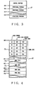
- Program memory 13 is composed of, for instance, a mask ROM. As shown in FIGURE 3, program memory 13 stores the control program for CPU 11 which provides functional programs which respond to a plurality of instruction data.
- Data memory 12 is used for storing various types of data, and is composed of, for instance, an EEPROM.
- data memory 12 is divided and defined into a plurality of areas, and each area is allotted an area number [00, 01, 02,..].
- AREA [00] 12a the respective area lead addresses and area sizes (the numbers of bytes which compose the areas) of all areas are stored corresponding to the area numbers. For instance, this operates in such a way that lead address A03 and area size S03 bytes correspond to AREA [03] 12d.
- AREA [01] 12b the lead address and control data of each functional program is stored corresponding to a function code.
- ID number data X0-X3 is stored in AREA [02] 12c.
- ID number data X0-X3 are used for verification of ID numbers. For instance, these are ID number data for the card-manufacturer, the card-issuer, the card-holder, etc.
- AREA [03] 12d, AREA [04] 12e and succeeding areas are respectively data areas.
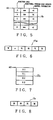
- FIGURE 6 shows the detail of the control data, which are stored in memory area 12bb of AREA [01] 12b, mentioned above.
- This is composed of identifiers Y0-Y3, W and ⁇ . That is, identifiers Y0-Y3 correspond to the above ID number data X0-X3 and indicate whether or not verification of these ID numbers data is required. For instance "1" represents 'required' and "0" represents 'not required'. For instance, if identifier Y0 is "1", this represents that verification of ID number data by ID number data X0 is required. Also, identifier W represents whether checking of identifiers Y0-Y3 is required. For instance "1" represents 'required' and "0” represents 'not required'.
- identifier a establishes whether all of the ID number verifications or only part of the ID number verifications is required. For instance, "1" represents 'all required' and "0" represents 'part only required'.
- FIGURE 8 shows the information which represent the result of the verification of ID numbers, and is composed of identifiers Z0-Z3. That is, identifiers Z0-Z3 correspond to respective ID number data X0-X3, and represent the verification results of these. For instance, “1" represents 'verification agreed' and "0" represents 'verification disagreed'. For instance, if identifier Z0 is "1", this represents that the result of ID number verification by ID number data X0 is 'verification agreed'. Also, this data, that is identifiers Z0-Z3, is stored in memory area 11a in the RAM which is housed in CPU 11.
- ID number verification operation is described with reference to the flow-chart shown in FIGURE 9.
- IC card 1 is in the ready state for instruction data from card reader/writer 2.
- CPU 11 judges whether or not this is ID number verifying instruction data (step S2). If it is ID number verifying instruction data, the ID number data to be collated (shown as PIN (Personal Identification Number) in the flow-chart) attributed to this instruction data is sequentially collated with each ID number data X0-X3 stored in area [02] of data memory 12 (steps S3, S5, S7 and S9).
- PIN Personal Identification Number
- CPU 11 sets the identifier (Z0-Z3) in the RAM which corresponds to the ID number data to "1" (steps S4, S6, S8 and S10). For instance, if PIN agrees with ID number data X0, identifier Z0 is set to "1" (step S4), and if PIN agrees with ID number data X3, identifier Z3 is set to "1" (step S10). Then, CPU 11 generates response data signifying 'verification agreed' to card reader/writer 2 (step S11), and returns to the ready for instruction data state. If, as the result of the above verification, there is no agreement with any of ID number data X0-X3, CPU 11 generates response data signifying 'verification disagreed' to card reader/writer 2 (step S12)., and returns to the ready for instruction data state.
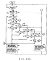
- IC card 1 is in the ready state for instruction data from card reader/writer 2.
- CPU 11 judges whether or not this is available instruction data (step S22). If it is not available instruction data, CPU 11 generates response data signifying 'undefined instruction data' to card reader/writer 2 (step S23) and returns to the ready for instruction data state. If the data is available instruction data, CPU 11 finds the function code attributed to the instruction data from area [01] of data memory 12.
- CPU 11 refers to the identifier W of the stored control information corresponding to that function code and judges whether W is "1" or not (step S24). If identifier W is not "1", checking of identifiers Y0-Y3 is not required (that is, ID number verification is not required). Thus, CPU 11 executes processing by a functional program corresponding to the relevant instruction data (step S25). That is, CPU 11 recognises the lead address of the functional program stored corresponding to the function code found from area [01] of data memory 12 and steps to that functional program. Then, processing is executed by that functional program, and the processing result is outputted to card reader/writer 2 as response data (step S26), and it returns to the ready for instruction data state.
- step S27 CPU 11 refers to the corresponding control data identifier Y0 (step S28). If identifier Y0 is "1”, CPU 11 refers to identifier Z0 of the data representing the result of the ID number verification (step S29), and judges whether this is "1" or not. If Z0 is "1", ID number verification has already been executed, and a verification agreed result has been obtained. In step S29, if Z0 is not "1", since a verification agreed result has not been obtained, response data signifying 'undefined instruction data' is outputted (step S23), and it enters the ready for instruction data state.
- step S28 if identifier Y0 is not “1”, CPU 11 refers to control data identifier Y1 (step S30), and if this is “1", CPU 11 refers to identifier Z1 representing the result of the ID number verification and judges whether this is "1" or not (step S31). If Z1 is "1", ID number verification has already been executed and a verification agreed result has been obtained. If Z1 is not “1”, since a verification agreed result has not been obtained, response data signifying 'undefined instruction data' is generated (step S23), and it enters the ready for instruction data state.
- step S30 if Y1 is not “1”, CPU 11 refers to control data identifier Y2 (step S32), and if this is “1”, CPU 11 refers to identifier Z2 and judges whether this is "1", or not (step S33). If Z2 is "1", ID number verification has already been executed and a verification agreed result has been obtained. If Z2 is not "1", since a verification agreed result has not been obtained, response data signifying 'undefined instruction data' is generated (step S23), and it enters the ready for instruction data state.
- step S32 if Y2 is not “1”, CPU 11 refers to control data identifier Y3 (step S34), and if this is “1", CPU 11 refers to identifier Z3 and judges whether this is "1", or not (step S35). If Z3 is "1", ID number verification has already been executed and a verification agreed result has been obtained. If Z3 is not "1", since a verification agreed result has not been obtained, response data signifying 'undefined instruction data' is generated(step S23), and it enters the ready for instruction data state.
- step S34 if Y3 is not "1", the flow steps to step S25 as the ID number verification is not required. That is, CPU 11 executes processing by a functional program corresponding to the relevant instruction data (step S25).
- step S27 if identifier ⁇ is "1", as shown in FIGURE 10B, CPU 11 refers to the corresponding control data identifiers Y0-Y3 (steps S41, S43, S45 and S47) and finds an identifier which is "1". If CPU 11 finds an identifier which is "1”, CPU 11 refers to the identifier (Z0-Z3) of the information representing the result of ID number verification corresponding to that identifier and judges whether it is "1", or not (steps S42, S44, S46 and S48). If each of Z0-Z3 is-"1", ID number verification has already been executed and a 'verification agreed' result has been obtained.
- CPU 11 executes processing by the functional program corresponding to the relevant instruction data as described above. If one of Z0-Z3 is not "1", either ID number verification has not been executed or, even if ID number verification has been executed, a 'verification disagreed' result has been obtained. Therefore, CPU 11 does not execute processing, and generates response data signifying 'undefined instruction data' to card reader/writer 2. It then returns to the ready for instruction data state.
- an IC card has been shown as an example of a portable electronic device.
- the present invention is not limited to a card-shaped device.
- it may be applied to block-shaped or pencil-shaped devices. Accordingly, it should be understood that the scope of the invention is limited only by the appended claims.
Landscapes
- Engineering & Computer Science (AREA)
- Business, Economics & Management (AREA)
- Physics & Mathematics (AREA)
- General Physics & Mathematics (AREA)
- Microelectronics & Electronic Packaging (AREA)
- Computer Networks & Wireless Communication (AREA)
- Accounting & Taxation (AREA)
- Strategic Management (AREA)
- General Business, Economics & Management (AREA)
- Theoretical Computer Science (AREA)
- Storage Device Security (AREA)
- Credit Cards Or The Like (AREA)
Claims (7)
- Dispositif électronique portatif comprenant : des premiers moyens de mémoire pour stocker (12a-12e) plusieurs données de numéro d'identification (X0-X3) ;des moyens (2) pour recevoir plusieurs données d'instruction dont des données d'instruction vérifiant le numéro d'identification à partir d'un dispositif externe ;des moyens (11) pour vérifier les données de numéro d'identification par les moyens de réception en référence aux données de numéro d'identification stockées dans les premiers moyens de mémoire, lorsque les moyens de réception reçoivent les données de numéro d'identification et les données d'instruction vérifiant le numéro d'identification ;des deuxièmes moyens de mémoire (11a) pour stocker les résultats de la vérification ; etdes moyens pour exécuter les données d'instruction en réponse aux résultats de la vérification, caractérisé par :des troisièmes moyens de mémoire (12aa-12ee) pour stocker des données de contrôle correspondant aux données d'instruction et représentant plusieurs identificateurs (Y0-Y3 ; α ; W) indiquant chacun si une vérification de numéro d'identification est exigée ou non et indiquant en outre si une vérification complète ou partielle de numéro d'identification est exigée ; etdes moyens pour consulter les résultats de la vérification (Z0-Z3) stockés dans les deuxièmes moyens de mémoire selon les données de contrôle stockées dans les troisièmes moyens de mémoire après réception des données d'instruction par les moyens de réception.
- Dispositif selon la revendication 1, dans lequel les identificateurs comprennent un premier identificateur (Y0-Y3) désignant lesquelles des données de numéro d'identification doivent être vérifiées parmi les données de numéro d'identification entrées, et un deuxième identificateur (a) indiquant si une vérification complète ou partielle du numéro d'identification est exigée par rapport aux données de numéro d'identification désignées par les premiers identificateurs (Y0-Y3).
- Dispositif selon la revendication 2, dans lequel les moyens de consultation consultent les résultats de la vérification des données de numéro d'identification à vérifier.
- Dispositif selon la revendication 1, dans lequel les premier, deuxième et troisième moyens de mémoire sont contenus dans un élément de mémoire de données.
- Dispositif selon la revendication 1, dans lequel les moyens de consultation et les moyens de vérification comprennent une unité centrale contenue dans le dispositif électronique portatif.
- Procédé de traitement de données au moyen d'un dispositif électronique portatif avec une mémoire ayant des première à troisième zones de mémoire, le procédé comprenant les étapes consistant à :stocker plusieurs données de numéro d'identification (X0-X3) dans la première zone (12a-12e) de la mémoire ; recevoir les données de numéro d'identification à partir d'un dispositif externe (2) ;vérifier les données de numéro d'identification reçues à l'étape de réception en référence aux données de numéro d'identification stockées dans la première zone de mémoire de la mémoire ;stocker les résultats de la vérification (Z0-Z3) dans la deuxième zone (11a) de la mémoire ;exécuter les données d'instruction en réponse aux résultats de la vérification ; recevoir les données d'instruction à partir du dispositif externe, caractérisé par les étapes consistant à :stocker, dans la troisième zone de mémoire de la mémoire, les données de contrôle correspondant aux données d'instruction et représentant plusieurs identificateurs (Y0-Y3 ; α ; W) indiquant chacun si la vérification du numéro d'identification est exigée ou non et indiquant en outre si une vérification complète ou partielle du numéro d'identification est exigée ; etconsulter les résultats de la vérification stockés dans la deuxième zone de mémoire de la mémoire selon les données de contrôle stockées dans la troisième zone de mémoire de la mémoire après réception des données d'instruction.
- Procédé selon la revendication 6, caractérisé en outre en ce que : les données de vérification du numéro d'identification sont reçues à partir du dispositif externe avec les données de numéro d'identification et stockées dans la première zone de mémoire avant l'étape de vérification des données de numéro d'identification et les résultats de la vérification sont stockés dans la deuxième zone de mémoire pour chaque élément de données d'instruction vérifiant le numéro d'identification ; et également caractérisé en ce que les étapes de stockage et de consultation comprennent les étapes consistant à :stocker, dans la troisième zone de mémoire de la mémoire, un premier identificateur (W) indiquant si la vérification du numéro d'identification est exigée ou non par rapport à chacune des données d'instruction, un deuxième identificateur (Y0-Y3) désignant les données de numéro d'identification à vérifier parmi la pluralité de données de numéro d'identification stockées dans la première zone de la mémoire, et un troisième identificateur (α) indiquant si une vérification complète ou partielle du numéro d'identification des données de numéro d'identification désignées par les deuxièmes identificateurs (Y0-Y3) est exigée ;consulter les résultats de la vérification des données de numéro d'identification à vérifier lorsque la vérification du numéro d'identification est exigée en se basant sur les premier à troisième identificateurs stockés dans la troisième zone de mémoire de la mémoire après réception des données d'instruction ; etexécuter les données d'instruction lorsque seules les données de numéro d'identification ont été vérifiées à l'étape de consultation.
Applications Claiming Priority (2)
| Application Number | Priority Date | Filing Date | Title |
|---|---|---|---|
| JP32526390A JP3251579B2 (ja) | 1990-11-29 | 1990-11-29 | 携帯可能電子装置 |
| JP325263/90 | 1990-11-29 |
Publications (2)
| Publication Number | Publication Date |
|---|---|
| EP0488720A1 EP0488720A1 (fr) | 1992-06-03 |
| EP0488720B1 true EP0488720B1 (fr) | 1996-10-30 |
Family
ID=18174864
Family Applications (1)
| Application Number | Title | Priority Date | Filing Date |
|---|---|---|---|
| EP91310998A Expired - Lifetime EP0488720B1 (fr) | 1990-11-29 | 1991-11-28 | Dispositif électronique portatif et méthode de traitement de données |
Country Status (3)
| Country | Link |
|---|---|
| EP (1) | EP0488720B1 (fr) |
| JP (1) | JP3251579B2 (fr) |
| DE (1) | DE69122944T2 (fr) |
Families Citing this family (4)
| Publication number | Priority date | Publication date | Assignee | Title |
|---|---|---|---|---|
| EP0634723A1 (fr) * | 1993-07-12 | 1995-01-18 | Angewandte Digital Elektronik GmbH | Prise de couplage de carte pour une unité d'interface de carte |
| GB9502864D0 (en) * | 1995-02-14 | 1995-04-05 | Digicash Bv | Cryptographic reduced instruction set processor |
| US5879823A (en) * | 1995-12-12 | 1999-03-09 | Kennametal Inc. | Coated cutting tool |
| DE60045294D1 (de) | 1999-06-14 | 2011-01-05 | Ntt Docomo Inc | Batterieeinheit und Ladegerät für ein drahtloses Telekommunikationsgerät |
Family Cites Families (5)
| Publication number | Priority date | Publication date | Assignee | Title |
|---|---|---|---|---|
| FR2503423A1 (fr) * | 1981-03-31 | 1982-10-08 | Flonic Sa | Systeme de cartes a memoire electronique pouvant etre rechargees a des valeurs fiduciaires |
| US5010237A (en) * | 1987-04-10 | 1991-04-23 | Casio Computer Co., Ltd. | IC card system for preventing unauthorized data alteration |
| DE3879269T2 (de) * | 1987-05-15 | 1993-10-21 | Oki Electric Ind Co Ltd | IC-Karten und Informationsspeicher dafür. |
| FR2618002B1 (fr) * | 1987-07-10 | 1991-07-05 | Schlumberger Ind Sa | Procede et systeme d'authentification de cartes a memoire electronique |
| JP2831660B2 (ja) * | 1988-08-26 | 1998-12-02 | 株式会社東芝 | 携帯可能電子装置 |
-
1990
- 1990-11-29 JP JP32526390A patent/JP3251579B2/ja not_active Expired - Lifetime
-
1991
- 1991-11-28 EP EP91310998A patent/EP0488720B1/fr not_active Expired - Lifetime
- 1991-11-28 DE DE69122944T patent/DE69122944T2/de not_active Expired - Lifetime
Also Published As
| Publication number | Publication date |
|---|---|
| JP3251579B2 (ja) | 2002-01-28 |
| DE69122944D1 (de) | 1996-12-05 |
| DE69122944T2 (de) | 1997-07-24 |
| JPH04205082A (ja) | 1992-07-27 |
| EP0488720A1 (fr) | 1992-06-03 |
Similar Documents
| Publication | Publication Date | Title |
|---|---|---|
| US5285200A (en) | Portable electronic device and a method for processing data therefore | |
| JP2856393B2 (ja) | 携帯可能電子装置 | |
| US4879645A (en) | Data processing device with high security of stored programs | |
| US4983816A (en) | Portable electronic device | |
| US4988855A (en) | Portable electronic apparatus | |
| JPH022475A (ja) | Icカード | |
| JP2935613B2 (ja) | Icカードおよびicカードシステム | |
| EP0743622B1 (fr) | Support de mémoire portable et système pour sa délivrance | |
| JP2557838B2 (ja) | Icカ−ド | |
| EP0488720A1 (fr) | Dispositif électronique portatif et méthode de traitement de données | |
| JPH05250526A (ja) | 携帯可能電子装置 | |
| JP2671213B2 (ja) | Icカード | |
| JPH0654507B2 (ja) | 携帯可能電子装置 | |
| JP2635601B2 (ja) | 携帯可能電子装置 | |
| JP2537200B2 (ja) | 携帯可能電子装置 | |
| JP2002342734A (ja) | 携帯可能電子装置およびその履歴データ記憶方法 | |
| JP2001202487A (ja) | 携帯可能電子装置およびキー照合方法 | |
| JP3048550B2 (ja) | Icカード用icチップ | |
| JPH0772891B2 (ja) | データ伝送方法 | |
| JP2618953B2 (ja) | 送信処理方法およびデータ記憶媒体およびicチップ | |
| JP2577369B2 (ja) | Icカ−ド | |
| JPH0734214B2 (ja) | Icカード | |
| JPH01223586A (ja) | Icカードテスト方式 | |
| JP2549639B2 (ja) | デ−タ伝送方法 | |
| JP2003223613A (ja) | Icカードのアプリケーション管理方法 |
Legal Events
| Date | Code | Title | Description |
|---|---|---|---|
| PUAI | Public reference made under article 153(3) epc to a published international application that has entered the european phase |
Free format text: ORIGINAL CODE: 0009012 |
|
| 17P | Request for examination filed |
Effective date: 19911213 |
|
| AK | Designated contracting states |
Kind code of ref document: A1 Designated state(s): DE FR |
|
| 17Q | First examination report despatched |
Effective date: 19950612 |
|
| GRAG | Despatch of communication of intention to grant |
Free format text: ORIGINAL CODE: EPIDOS AGRA |
|
| GRAG | Despatch of communication of intention to grant |
Free format text: ORIGINAL CODE: EPIDOS AGRA |
|
| GRAH | Despatch of communication of intention to grant a patent |
Free format text: ORIGINAL CODE: EPIDOS IGRA |
|
| GRAH | Despatch of communication of intention to grant a patent |
Free format text: ORIGINAL CODE: EPIDOS IGRA |
|
| GRAA | (expected) grant |
Free format text: ORIGINAL CODE: 0009210 |
|
| AK | Designated contracting states |
Kind code of ref document: B1 Designated state(s): DE FR |
|
| ET | Fr: translation filed | ||
| REF | Corresponds to: |
Ref document number: 69122944 Country of ref document: DE Date of ref document: 19961205 |
|
| PLBE | No opposition filed within time limit |
Free format text: ORIGINAL CODE: 0009261 |
|
| STAA | Information on the status of an ep patent application or granted ep patent |
Free format text: STATUS: NO OPPOSITION FILED WITHIN TIME LIMIT |
|
| 26N | No opposition filed | ||
| PGFP | Annual fee paid to national office [announced via postgrant information from national office to epo] |
Ref country code: FR Payment date: 20101123 Year of fee payment: 20 |
|
| PGFP | Annual fee paid to national office [announced via postgrant information from national office to epo] |
Ref country code: DE Payment date: 20101124 Year of fee payment: 20 |
|
| REG | Reference to a national code |
Ref country code: DE Ref legal event code: R071 Ref document number: 69122944 Country of ref document: DE |
|
| REG | Reference to a national code |
Ref country code: DE Ref legal event code: R071 Ref document number: 69122944 Country of ref document: DE |
|
| PG25 | Lapsed in a contracting state [announced via postgrant information from national office to epo] |
Ref country code: DE Free format text: LAPSE BECAUSE OF EXPIRATION OF PROTECTION Effective date: 20111129 |