EP0489260B1 - Unterbrechungssteuerung - Google Patents
Unterbrechungssteuerung Download PDFInfo
- Publication number
- EP0489260B1 EP0489260B1 EP91118767A EP91118767A EP0489260B1 EP 0489260 B1 EP0489260 B1 EP 0489260B1 EP 91118767 A EP91118767 A EP 91118767A EP 91118767 A EP91118767 A EP 91118767A EP 0489260 B1 EP0489260 B1 EP 0489260B1
- Authority
- EP
- European Patent Office
- Prior art keywords
- signal
- interrupt request
- interrupt
- output
- timing
- Prior art date
- Legal status (The legal status is an assumption and is not a legal conclusion. Google has not performed a legal analysis and makes no representation as to the accuracy of the status listed.)
- Expired - Lifetime
Links
Images


Classifications
-
- G—PHYSICS
- G06—COMPUTING OR CALCULATING; COUNTING
- G06F—ELECTRIC DIGITAL DATA PROCESSING
- G06F13/00—Interconnection of, or transfer of information or other signals between, memories, input/output devices or central processing units
- G06F13/14—Handling requests for interconnection or transfer
- G06F13/20—Handling requests for interconnection or transfer for access to input/output bus
- G06F13/24—Handling requests for interconnection or transfer for access to input/output bus using interrupt
- G06F13/26—Handling requests for interconnection or transfer for access to input/output bus using interrupt with priority control
-
- G—PHYSICS
- G06—COMPUTING OR CALCULATING; COUNTING
- G06F—ELECTRIC DIGITAL DATA PROCESSING
- G06F13/00—Interconnection of, or transfer of information or other signals between, memories, input/output devices or central processing units
- G06F13/14—Handling requests for interconnection or transfer
- G06F13/20—Handling requests for interconnection or transfer for access to input/output bus
- G06F13/24—Handling requests for interconnection or transfer for access to input/output bus using interrupt
Definitions
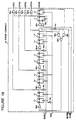
- FIG. 1 there is shown block diagram of a typical usual microcomputer.
- the shown microcomputer includes a CPU (central processing unit) 100, a memory block 200, an interrupt controller 300, and a peripheral function block 400, which are coupled to each other by an internal data bus and other signal lines and buses.
- An instruction is read out from a program memory within the memory block 200, and executed by the CPU 100.
- the peripheral function block 400 is controlled to access to the CPU 100 through the internal data bus so as to write data to the CPU and to read data from CPU.
- the peripheral function block 400 operates independently upon the CPU 100.
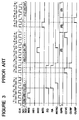
- the timing signals STG1, STG2, STG3 are sequentially outputted by alternately repeating "1" and "0".
- the interrupt request signal INT1 is brought into “1”
- the content of the interrupt request flag register 32 is brought into “1”.
- the output of the AND gate AG21 of the acknowledged interrupt request controller 4 is maintained at “0”.
- the output of the AND gate AG12 in the interrupt request signal controllers 3A, 3C and 3D are maintained at "0", "0" and "0", respectively. Therefore, the CM1 signal is maintained at "1".
- the RA signal is brought to "1". Since the priority bit register 33B is "1", the output of the AND gate AG14 becomes “0", and therefore, the CM2 signal becomes “1". Since the CM2 signal is "1" and the output of the inverter IV12 is “0”, the output of the AND gate AG15 is “0”, and therefore, the RS latch circuit 34 is not reset. Since the RA signal corresponding to the interrupt request signal INT1 is "1", when the timing clock CLK becomes “0”, the latch circuit 9 is brought into “1”. In addition, when the timing signal STG3 becomes “1", the output of the NAND gate NAG1 is brought into “0”, and therefore, the SLPRH signal is maintained at "1".
- the timing signal STG0 is generated. Since the timing signal STG0 is "1" and the output of the latch circuit 9 becomes “1”, the interrupt processing request signal INTRQ becomes "1", so that an interrupt processing is required to the CPU 100.
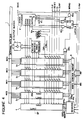
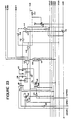
- FIG. 9 there is shown a block diagram of a second embodiment of the interrupt controller in accordance with the present invention.
- the stage counter 2A shown in Figure 10 is different in construction from the stage counter 2 shown in Figure 5, in that AND gates AG28 and AG29, an inverter IV25 and latch circuits L9 and L10 are added, and a timing signal STG4 is added as one output signal.
- the stage counter 2A operates similarly to the stage counter 2 shown in Figure 2, but since the timing signal STG4 is generated next to the timing signal STG4, the scan signal is generate in a manner of STG1 ⁇ STG2 ⁇ STG3 ⁇ STG4 ⁇ STG1 ⁇ .
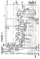
- the output of the latch 42 of the acknowledged interrupt request controller 4 is "0", and therefore, the output of the AND gate AG25 is “0" and the output of the inverter IV21 is also "0". Accordingly, the the N-channel MOS transistor Q21 is in a turned-on condition. Similarly, the N-channel MOS transistor 544 of the disable inhibition interrupt request controller 4B is also in in a turned-on condition. Thus, the output signal CMOT of the interrupt request signal controller 3A is grounded and therefore is brought into "0". On the other hand, the input signal CMIN of the interrupt request signal controller 3A and the output CMOT and the input signal CMIN of the interrupt request signal controller 3A are "1".
- the latch circuit 48A latches the output of the QR gate OG1 at the timing signal STG1 when the timing clock CLK is "0", and becomes to output the latched data in response to the next timing clock.
- the latch circuit 48A outputs an MSINTRQ signal through an AND gate 49 at the timing signal STG0.
- This MSINTRQ signal is a macro-service interrupt processing request signal to the CPU 100.
- the latch circuit 48A is reset to "0" by the reset signal RESET, the CLRIF signal and the CLRMS signal.
- the CLRMS signal is generated in the execution of the macro-services, for clearing a processing designation bit latch 160 (MSINT bit) designating the interrupt by the macro-service.
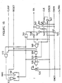
- a latch circuit 321 is initialized to "1" at the timing of "0" of the timing clock CLK, and similarly, latch circuits 323 and 325 are initialized to "0" and a RS type latch 327 is initialized to "0". Accordingly, at the timing of "1" of a next timing clock CLK, a latch circuit 322 is brought to “1”, and latch circuits 324 and 326 are brought to "0".
- FIG 22 there is shown a logic circuit diagram of the interrupt request signal controller 3A shown in Figure 20. Since the interrupt request signal controllers 3A to 3D have the same construction, only the interrupt request signal controller 3A is shown.
- An output of an AND gate 132 is brought into “1” when the priority bit register 117 is “1", the CM2 signal is “0” and the timing signal STG2 is “1".
- An output of an AND gate 149 is brought into “1” at the timing of "0" of the timing clock CLK when the RA signal is “0” and the timing signal STG3 is “1”.
- the interrupt controller can respond to the interrupt request at a speed higher than that of the conventional interrupt controller.
- an interrupt request having the same priority level as that of the interrupt processing being currently executed is generated, and when two or more interrupt requests having the same priority level are simultaneously generated, an interrupt request having a high default (high in the order of preference set by a circuit) is acknowledged, but an interrupt request having a low default is not acknowledged.
- the fifth embodiment can comply with the macro-service processing. Therefore, the interrupt controller as mentioned above can flexibly comply with various interrupt requests at a high speed.
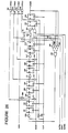
- FIG. 34 there is shown a block diagram of an eighth embodiment of the interrupt controller in accordance with the present invention.
Landscapes
- Engineering & Computer Science (AREA)
- Theoretical Computer Science (AREA)
- Physics & Mathematics (AREA)
- General Engineering & Computer Science (AREA)
- General Physics & Mathematics (AREA)
- Bus Control (AREA)
- Communication Control (AREA)
Claims (5)
- Unterbrechungssteuerung, die folgendes aufweist: eine Vielzahl von n-Bit-Prioritätsbit-Registern zum Zuordnen von 2n Prioritätspegeln zu einer Vielzahl von Unterbrechungs-Anfragesignalen (wobei n eine ganze Zahl nicht kleiner als 2 ist), einen Stufenzähler zum sequentiellen und wiederholten Erzeugen von (n+1) Zeitgabesignalen, die zum Abtasten der Prioritätspegel der Unterbrechungs-Anfragesignale verwendet werden, ein Register für Prioritätspegel während einer Ausführung zum Speichern des Inhalts des Prioritätsbit-Registers des Unterbrechungs-Anfragesignals entsprechend einer gerade ausgeführten Unterbrechungsverarbeitung, eine Unterbrechungs-Anfragesignal-Steuereinrichtung zum Vergleichen des Inhalts des Registers für Prioritätspegel während einer Ausführung mit Inhalten der Prioritätsbit-Register der erzeugten Unterbrechungs-Anfragesignale einschließlich des Prioritätsbit-Registers des Unterbrechungs-Anfragesignals entsprechend der gerade ausgeführten Unterbrechungsverarbeitung synchron zu den "n" Zeitgabesignalen in der Reihenfolge des Bits an der höchsten Stelle zum Bit an der niedrigsten Stelle, wobei die Unterbrechungs-Anfragesignal-Steuereinrichtung arbeitet, um ein Unterbrechungs-Anfragesignal mit dem Bit höchster Priorität aus den gerade erzeugten Unterbrechungs-Anfragesignalen zu erfassen, wobei die Unterbrechungs-Anfragesignal-Steuereinrichtung auch derart arbeitet, daß dann, wenn eine Vielzahl von Unterbrechungs-Anfragesignalen mit dem Bit höchster Priorität erfaßt wird, die Unterbrechungs-Anfragesignal-Steuereinrichtung ein Unterbrechungs-Anfragesignal gemäß einer vorbestimmten Reihenfolge synchron zu einem Zeitgabesignal auswählt, das den "n" Zeitgabesignalen folgt, und eine Einrichtung zum Erzeugen eines Unterbrechungsverarbeitungs-Anfragesignals, wenn die Unterbrechungs-Anfragesignal-Steuereinrichtung ein Unterbrechungs-Anfragesignal mit dem höchsten Prioritätspegel erfaßt.
- Unterbrechungssteuerung nach Anspruch 1, wobei die jeweiligen Bits des Prioritätsbit-Registers derart eingestellt sind, daß sie eine Gewichtung von 2(N-1) haben (wobei N = 1 bis n gilt).
- Unterbrechungssteuerung nach Anspruch 2, wobei der Inhalt des Prioritätsbit-Registers in der Reihenfolge von einem Bit mit großer Gewichtung zu einem Bit mit geringer Gewichtung erfaßt wird.
- Unterbrechungssteuerung nach Anspruch 1, die weiterhin eine Unterbrechungssperrverhinderungs-Unterbrechungs-Anfragesignalsteuerung zum Erfassen eines eingegebenen Unterbrechungssperrverhinderungs-Unterbrechungs-Anfragesignals in der vorbestimmten Reihenfolge mit einer einzigen Zeitgabe enthält.
- Unterbrechungssteuerung nach Anspruch 1, die weiterhin eine Verarbeitungs-Zuordnungseinrichtung zum Zuordnen einer aus einer Vektorunterbrechungsverarbeitung und einer Makrodienstverarbeitung ausgewählten Verarbeitung enthält.
Applications Claiming Priority (8)
| Application Number | Priority Date | Filing Date | Title |
|---|---|---|---|
| JP2297475A JP2567988B2 (ja) | 1990-11-02 | 1990-11-02 | 割込みコントローラ |
| JP297475/90 | 1990-11-02 | ||
| JP2411473A JP2702291B2 (ja) | 1990-12-18 | 1990-12-18 | 割込みコントローラ |
| JP411473/90 | 1990-12-18 | ||
| JP411472/90 | 1990-12-18 | ||
| JP2411472A JP2702290B2 (ja) | 1990-12-18 | 1990-12-18 | 割込みコントローラ |
| JP12911/91 | 1991-01-09 | ||
| JP3012911A JPH04235635A (ja) | 1991-01-09 | 1991-01-09 | 割込みコントローラ |
Publications (3)
| Publication Number | Publication Date |
|---|---|
| EP0489260A2 EP0489260A2 (de) | 1992-06-10 |
| EP0489260A3 EP0489260A3 (en) | 1992-08-05 |
| EP0489260B1 true EP0489260B1 (de) | 1996-04-17 |
Family
ID=27455896
Family Applications (1)
| Application Number | Title | Priority Date | Filing Date |
|---|---|---|---|
| EP91118767A Expired - Lifetime EP0489260B1 (de) | 1990-11-02 | 1991-11-04 | Unterbrechungssteuerung |
Country Status (4)
| Country | Link |
|---|---|
| US (1) | US5481729A (de) |
| EP (1) | EP0489260B1 (de) |
| KR (1) | KR950014373B1 (de) |
| DE (1) | DE69118833T2 (de) |
Families Citing this family (4)
| Publication number | Priority date | Publication date | Assignee | Title |
|---|---|---|---|---|
| EP0704806B1 (de) * | 1994-09-28 | 2001-01-24 | STMicroelectronics S.r.l. | Steuerungseinheit für Unterbrechungskanäle in einem Mikrokontroller |
| KR100313945B1 (ko) * | 1999-03-03 | 2001-11-15 | 김영환 | 다단 인터럽트 제어 장치 |
| US9563590B2 (en) * | 2014-03-17 | 2017-02-07 | Nxp Usa, Inc. | Devices with arbitrated interface busses, and methods of their operation |
| US9361027B1 (en) * | 2014-12-16 | 2016-06-07 | Texas Instruments Incorporated | System and method for fast modification of register content |
Family Cites Families (14)
| Publication number | Priority date | Publication date | Assignee | Title |
|---|---|---|---|---|
| US4091447A (en) * | 1976-07-19 | 1978-05-23 | Union Carbide Corporation | Interrupt control system for a microcomputer |
| DE2659662C3 (de) * | 1976-12-30 | 1981-10-08 | Ibm Deutschland Gmbh, 7000 Stuttgart | Prioritätsstufengesteuerte Unterbrechungseinrichtung |
| US4271468A (en) * | 1979-11-06 | 1981-06-02 | International Business Machines Corp. | Multiprocessor mechanism for handling channel interrupts |
| IT1129371B (it) * | 1980-11-06 | 1986-06-04 | Cselt Centro Studi Lab Telecom | Commutatore di messaggi a struttura distribuita su canale ad accesso casuale per colloquio a messaggi tra unita elaborative |
| US4689739A (en) * | 1983-03-28 | 1987-08-25 | Xerox Corporation | Method for providing priority interrupts in an electrophotographic machine |
| US4807117A (en) * | 1983-07-19 | 1989-02-21 | Nec Corporation | Interruption control apparatus |
| US4633394A (en) * | 1984-04-24 | 1986-12-30 | International Business Machines Corp. | Distributed arbitration for multiple processors |
| JPS619748A (ja) * | 1984-06-25 | 1986-01-17 | Nec Corp | 入出力制御装置 |
| US4734882A (en) * | 1985-04-01 | 1988-03-29 | Harris Corp. | Multilevel interrupt handling scheme |
| US4761732A (en) * | 1985-11-29 | 1988-08-02 | American Telephone And Telegraph Company, At&T Bell Laboratories | Interrupt controller arrangement for mutually exclusive interrupt signals in data processing systems |
| JPS63238630A (ja) * | 1987-03-26 | 1988-10-04 | Toshiba Corp | マイクロプロセツサの割込み制御装置 |
| JPH0212432A (ja) * | 1988-06-30 | 1990-01-17 | Nec Corp | データ処理装置 |
| DE68905028T2 (de) * | 1988-11-17 | 1993-11-11 | Nippon Electric Co | Datenverarbeitungseinrichtung zur Erzeugung einer Folge von Impulsen die eine variable Länge an den Ausgängen aufweisen. |
| JP2855298B2 (ja) * | 1990-12-21 | 1999-02-10 | インテル・コーポレーション | 割込み要求の仲裁方法およびマルチプロセッサシステム |
-
1991
- 1991-11-02 KR KR1019910019547A patent/KR950014373B1/ko not_active Expired - Fee Related
- 1991-11-04 DE DE69118833T patent/DE69118833T2/de not_active Expired - Fee Related
- 1991-11-04 EP EP91118767A patent/EP0489260B1/de not_active Expired - Lifetime
-
1993
- 1993-08-23 US US08/110,495 patent/US5481729A/en not_active Expired - Lifetime
Also Published As
| Publication number | Publication date |
|---|---|
| KR950014373B1 (ko) | 1995-11-25 |
| KR920010462A (ko) | 1992-06-26 |
| DE69118833T2 (de) | 1997-01-02 |
| EP0489260A3 (en) | 1992-08-05 |
| EP0489260A2 (de) | 1992-06-10 |
| US5481729A (en) | 1996-01-02 |
| DE69118833D1 (de) | 1996-05-23 |
Similar Documents
| Publication | Publication Date | Title |
|---|---|---|
| US4034349A (en) | Apparatus for processing interrupts in microprocessing systems | |
| US4967398A (en) | Read/write random access memory with data prefetch | |
| EP0355560B1 (de) | Bedingungsschreib-RAM | |
| US6101584A (en) | Computer system and semiconductor device on one chip including a memory and central processing unit for making interlock access to the memory | |
| US4797853A (en) | Direct memory access controller for improved system security, memory to memory transfers, and interrupt processing | |
| US4112490A (en) | Data transfer control apparatus and method | |
| US4152761A (en) | Multi-task digital processor employing a priority | |
| US4366538A (en) | Memory controller with queue control apparatus | |
| US5115510A (en) | Multistage data flow processor with instruction packet, fetch, storage transmission and address generation controlled by destination information | |
| EP0437276A2 (de) | Mikrorechner und Verfahren zur Buszyklussteuerung | |
| EP0183231A2 (de) | Datenprozessor | |
| US4924427A (en) | Direct memory access controller with direct memory to memory transfers | |
| US4384342A (en) | System for reducing access time to plural memory modules using five present-fetch and one prefetch address registers | |
| US4451880A (en) | Memory controller with interleaved queuing apparatus | |
| EP0432575A2 (de) | Datenprozessor mit Wartezustandsteuerungseinheit | |
| EP0489260B1 (de) | Unterbrechungssteuerung | |
| EP0408353A2 (de) | Integrierte Halbleiterschaltung | |
| US4853848A (en) | Block access system using cache memory | |
| US5559985A (en) | Cache memory having improved hit ratio by selecting the number of bus cycles required for block replacement | |
| JP2567988B2 (ja) | 割込みコントローラ | |
| JP2000148588A (ja) | アドレス変換テーブル付きメモリ | |
| US4503498A (en) | Multiprocessor cratecontroller | |
| JPS5911945B2 (ja) | 計算装置の操作方法 | |
| EP0335494A2 (de) | Zeitüberwachungseinrichtung | |
| JP2702291B2 (ja) | 割込みコントローラ |
Legal Events
| Date | Code | Title | Description |
|---|---|---|---|
| PUAI | Public reference made under article 153(3) epc to a published international application that has entered the european phase |
Free format text: ORIGINAL CODE: 0009012 |
|
| AK | Designated contracting states |
Kind code of ref document: A2 Designated state(s): DE FR GB IT |
|
| PUAL | Search report despatched |
Free format text: ORIGINAL CODE: 0009013 |
|
| 17P | Request for examination filed |
Effective date: 19920427 |
|
| AK | Designated contracting states |
Kind code of ref document: A3 Designated state(s): DE FR GB IT |
|
| 17Q | First examination report despatched |
Effective date: 19950630 |
|
| GRAA | (expected) grant |
Free format text: ORIGINAL CODE: 0009210 |
|
| AK | Designated contracting states |
Kind code of ref document: B1 Designated state(s): DE FR GB IT |
|
| REF | Corresponds to: |
Ref document number: 69118833 Country of ref document: DE Date of ref document: 19960523 |
|
| ITF | It: translation for a ep patent filed | ||
| ET | Fr: translation filed | ||
| GRAH | Despatch of communication of intention to grant a patent |
Free format text: ORIGINAL CODE: EPIDOS IGRA |
|
| PLBE | No opposition filed within time limit |
Free format text: ORIGINAL CODE: 0009261 |
|
| STAA | Information on the status of an ep patent application or granted ep patent |
Free format text: STATUS: NO OPPOSITION FILED WITHIN TIME LIMIT |
|
| 26N | No opposition filed | ||
| REG | Reference to a national code |
Ref country code: GB Ref legal event code: IF02 |
|
| PGFP | Annual fee paid to national office [announced via postgrant information from national office to epo] |
Ref country code: GB Payment date: 20021030 Year of fee payment: 12 |
|
| PGFP | Annual fee paid to national office [announced via postgrant information from national office to epo] |
Ref country code: DE Payment date: 20021107 Year of fee payment: 12 |
|
| REG | Reference to a national code |
Ref country code: GB Ref legal event code: 732E |
|
| REG | Reference to a national code |
Ref country code: FR Ref legal event code: TP |
|
| PG25 | Lapsed in a contracting state [announced via postgrant information from national office to epo] |
Ref country code: GB Free format text: LAPSE BECAUSE OF NON-PAYMENT OF DUE FEES Effective date: 20031104 |
|
| PG25 | Lapsed in a contracting state [announced via postgrant information from national office to epo] |
Ref country code: DE Free format text: LAPSE BECAUSE OF NON-PAYMENT OF DUE FEES Effective date: 20040602 |
|
| GBPC | Gb: european patent ceased through non-payment of renewal fee |
Effective date: 20031104 |
|
| PG25 | Lapsed in a contracting state [announced via postgrant information from national office to epo] |
Ref country code: IT Free format text: LAPSE BECAUSE OF NON-PAYMENT OF DUE FEES;WARNING: LAPSES OF ITALIAN PATENTS WITH EFFECTIVE DATE BEFORE 2007 MAY HAVE OCCURRED AT ANY TIME BEFORE 2007. THE CORRECT EFFECTIVE DATE MAY BE DIFFERENT FROM THE ONE RECORDED. Effective date: 20051104 |
|
| PGFP | Annual fee paid to national office [announced via postgrant information from national office to epo] |
Ref country code: FR Payment date: 20061108 Year of fee payment: 16 |
|
| REG | Reference to a national code |
Ref country code: FR Ref legal event code: ST Effective date: 20080930 |
|
| PG25 | Lapsed in a contracting state [announced via postgrant information from national office to epo] |
Ref country code: FR Free format text: LAPSE BECAUSE OF NON-PAYMENT OF DUE FEES Effective date: 20071130 |