EP0489384A2 - Verfahren zur Orientierung mindestens eines auf einer Leiterplatte aufgesetzten elektronischen Bauelementes - Google Patents
Verfahren zur Orientierung mindestens eines auf einer Leiterplatte aufgesetzten elektronischen Bauelementes Download PDFInfo
- Publication number
- EP0489384A2 EP0489384A2 EP91120661A EP91120661A EP0489384A2 EP 0489384 A2 EP0489384 A2 EP 0489384A2 EP 91120661 A EP91120661 A EP 91120661A EP 91120661 A EP91120661 A EP 91120661A EP 0489384 A2 EP0489384 A2 EP 0489384A2
- Authority
- EP
- European Patent Office
- Prior art keywords
- circuit board
- printed circuit
- contact points
- electronic components
- printed
- Prior art date
- Legal status (The legal status is an assumption and is not a legal conclusion. Google has not performed a legal analysis and makes no representation as to the accuracy of the status listed.)
- Granted
Links
Images

Classifications
-
- H—ELECTRICITY
- H05—ELECTRIC TECHNIQUES NOT OTHERWISE PROVIDED FOR
- H05K—PRINTED CIRCUITS; CASINGS OR CONSTRUCTIONAL DETAILS OF ELECTRIC APPARATUS; MANUFACTURE OF ASSEMBLAGES OF ELECTRICAL COMPONENTS
- H05K10/00—Arrangements for improving the operating reliability of electronic equipment, e.g. by providing a similar standby unit
-
- H—ELECTRICITY
- H05—ELECTRIC TECHNIQUES NOT OTHERWISE PROVIDED FOR
- H05K—PRINTED CIRCUITS; CASINGS OR CONSTRUCTIONAL DETAILS OF ELECTRIC APPARATUS; MANUFACTURE OF ASSEMBLAGES OF ELECTRICAL COMPONENTS
- H05K1/00—Printed circuits
- H05K1/02—Details
- H05K1/14—Structural association of two or more printed circuits
- H05K1/141—One or more single auxiliary printed circuits mounted on a main printed circuit, e.g. modules, adapters
-
- H—ELECTRICITY
- H05—ELECTRIC TECHNIQUES NOT OTHERWISE PROVIDED FOR
- H05K—PRINTED CIRCUITS; CASINGS OR CONSTRUCTIONAL DETAILS OF ELECTRIC APPARATUS; MANUFACTURE OF ASSEMBLAGES OF ELECTRICAL COMPONENTS
- H05K1/00—Printed circuits
- H05K1/02—Details
- H05K1/14—Structural association of two or more printed circuits
- H05K1/148—Arrangements of two or more hingeably connected rigid printed circuit boards, i.e. connected by flexible means
-
- H—ELECTRICITY
- H05—ELECTRIC TECHNIQUES NOT OTHERWISE PROVIDED FOR
- H05K—PRINTED CIRCUITS; CASINGS OR CONSTRUCTIONAL DETAILS OF ELECTRIC APPARATUS; MANUFACTURE OF ASSEMBLAGES OF ELECTRICAL COMPONENTS
- H05K2201/00—Indexing scheme relating to printed circuits covered by H05K1/00
- H05K2201/09—Shape and layout
- H05K2201/09009—Substrate related
- H05K2201/0909—Preformed cutting or breaking line
-
- H—ELECTRICITY
- H05—ELECTRIC TECHNIQUES NOT OTHERWISE PROVIDED FOR
- H05K—PRINTED CIRCUITS; CASINGS OR CONSTRUCTIONAL DETAILS OF ELECTRIC APPARATUS; MANUFACTURE OF ASSEMBLAGES OF ELECTRICAL COMPONENTS
- H05K2201/00—Indexing scheme relating to printed circuits covered by H05K1/00
- H05K2201/10—Details of components or other objects attached to or integrated in a printed circuit board
- H05K2201/10007—Types of components
- H05K2201/10106—Light emitting diode [LED]
-
- H—ELECTRICITY
- H05—ELECTRIC TECHNIQUES NOT OTHERWISE PROVIDED FOR
- H05K—PRINTED CIRCUITS; CASINGS OR CONSTRUCTIONAL DETAILS OF ELECTRIC APPARATUS; MANUFACTURE OF ASSEMBLAGES OF ELECTRICAL COMPONENTS
- H05K2201/00—Indexing scheme relating to printed circuits covered by H05K1/00
- H05K2201/10—Details of components or other objects attached to or integrated in a printed circuit board
- H05K2201/10227—Other objects, e.g. metallic pieces
- H05K2201/10287—Metal wires as connectors or conductors
-
- H—ELECTRICITY
- H05—ELECTRIC TECHNIQUES NOT OTHERWISE PROVIDED FOR
- H05K—PRINTED CIRCUITS; CASINGS OR CONSTRUCTIONAL DETAILS OF ELECTRIC APPARATUS; MANUFACTURE OF ASSEMBLAGES OF ELECTRICAL COMPONENTS
- H05K2201/00—Indexing scheme relating to printed circuits covered by H05K1/00
- H05K2201/10—Details of components or other objects attached to or integrated in a printed circuit board
- H05K2201/10431—Details of mounted components
- H05K2201/10439—Position of a single component
- H05K2201/10477—Inverted
-
- H—ELECTRICITY
- H05—ELECTRIC TECHNIQUES NOT OTHERWISE PROVIDED FOR
- H05K—PRINTED CIRCUITS; CASINGS OR CONSTRUCTIONAL DETAILS OF ELECTRIC APPARATUS; MANUFACTURE OF ASSEMBLAGES OF ELECTRICAL COMPONENTS
- H05K3/00—Apparatus or processes for manufacturing printed circuits
- H05K3/0011—Working of insulating substrates or insulating layers
- H05K3/0044—Mechanical working of the substrate, e.g. drilling or punching
- H05K3/0052—Depaneling, i.e. dividing a panel into circuit boards; Working of the edges of circuit boards
Definitions
- the invention relates to the field of printed circuit boards and more particularly to a method for orienting at least one electronic component placed on a printed circuit board.
- Printed circuit boards generally have an insulating plate comprising two faces.
- the first face allows linear printing, for example by screen printing, of conductive tracks and the second face ensures the reception of the electronic components which are connected to the conductive tracks of the first face by means of metallized holes made in the insulating plate.
- said printed circuit board cannot support all the components on the same face.
- indicator lights are used to display the operating states of the microwave oven on the display panel serving the user.
- the printed circuit board must be pressed against the internal face of the box placed on the front face of the microwave oven. This operation is not feasible due in particular to the thickness of certain components, thus, an adaptation must be carried out.
- the LEDs luminous 1 are mounted on a first printed circuit card 2, this so-called card is fixed by fastening elements 3 on a second printed circuit card 4 which controls the operation of the microwave oven and on which electronic components are fixed 6
- the fastening elements are, for example, four in number, this number being in no way limiting.
- the first printed circuit board 2 is electrically connected to the second printed circuit board 4 by connection wires 5.
- the connection between each of the printed circuit boards is made at the periphery of each of said boards.
- the indicator lights 1 of the first printed circuit board 2 and the electronic components 6 of the second printed circuit board 4 are on the outer faces of the two printed circuit boards placed opposite. In this way, the indicator lights 1 of the first printed circuit board 2 can be pressed to the location determined on the front face of the housing of the microwave oven.
- the system thus used is bulky, difficult to produce and expensive.
- the object of the invention is to remedy these drawbacks by implementing a method for orienting at least one electronic component of a portion of a printed circuit board, which is quick to manufacture and economical.
- a printed circuit board comprises an insulating plate 8.
- the insulating plate 8 is, for example, rectangular and has four sides 11, 12, 13, and 14.
- One of the sides 11 of the plate 8 has a pre-cut 15, each of the sides (11 or 12 or 13 or 14) may include several pre-cuts.
- the pre-cut 15 corresponds to a portion of the printed circuit board which supports, after implantation of the components, an electronic component, for example, an indicator light 1; said card portion can also support several electronic components.
- This portion 15 is pre-cut over a length L and a width 1 corresponding respectively to the length and to the maximum width of pre-cut on the printed circuit board.
- the shape of this portion 15 is, for example, rectangular.
- pre-cutting for example, circular or square
- the pre-cut portion 15 is held on the printed circuit board, for example, by two weakenable sections 30 and 31, one of the main characteristics of which is to resist breakage during the implantation of the electronic components.
- the portion of printed circuit board 15 of rectangular shape is delimited by a segment AA comprising four sections AF, FG, GP and PA.
- the AF section includes two flat parts AB and EF parallel to the periphery of the sides 11 and 13 and a solid rectangular part BCDE whose sides BC and DE are parallel to the sides 12 and 14 and the sides CD and BE are parallel to the sides 11 and 13.
- the sections FG and PA are parallel to the sides 12 and 14.
- the GP section includes three flat parts GH, KL and NP, and two solid rectangular parts HIJK and LMNO whose sides HI, JK, LM and NO are parallel to sides 11 and 13.
- the positioning of the rectangular parts HIJK and LMNO corresponding to the two sections embrittlement 30 and 31 as well as the dimensions of these said parts determine the positioning and the dimensions of the solid rectangular part BCDE.
- the portions intended to come into look of said sections must be hollow that is to say absence of material (not shown in the Figure) or flat as the parts AB and EF.
- the solid rectangular part BCDE has a length CD less than the length KL and a width BC less than the width LM.
- the pre-cut rectangular portion 15 on which the conductive tracks are printed also includes two contact points 16 and 17; these contact points 16 and 17 are, for example, metallized holes made in the insulating plate 8 and in direct connection with the conductive tracks made on the portion 15 and appearing on the other side (not shown) of the insulating plate 8.
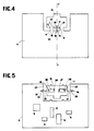
- Two other contact points 18 and 19 are formed on the printed circuit board on the sides 22 and 23; these contact points are, for example, metallized holes made in the insulating plate 8 and in direct connection with the conductive tracks of the printed circuit board. All the contact points 16, 17, 18 and 19 are positioned, for example, on a single axis XX '. In FIG.
- a printed circuit board comprising an insulating plate 8 and pre-cut according to the invention, is shown after implantation of the electronic components 6 including an indicator light 1 which will be called “led” in the following description and positioned on the pre-cut portion 15.
- an indicator light 1 which will be called “led” in the following description and positioned on the pre-cut portion 15.
- two electrical wires 20 and 21 each having two ends are located respectively between the contact points 16 and 17 of the portion 15 and the contact points 18 and 19 of the printed circuit board 7.
- One end 20a of the electric wire 20 is connected to the contact point 18 of the printed circuit board 7 and the other end 20b of the said wire 20 is connected to the contact point 16 of the portion of a printed circuit board 15.
- the end 21a of the electric wire 21 is connected to the contact point 19 of the printed circuit board 8 and the other end 21b of the said wire 21 is connected to the contact point 17 of the portion 15.
- the contact points 16 and 17 of the printed circuit board portion 15 are located respectively at the half-length of the parts PA and FG and the contact points 18 and 19 of the printed circuit board 8 are located opposite -vis points 16 and 17 so that all the contact points are aligned.
- the position of the contact points 16, 17, 18 and 19 is determined so that the portion 15 can rotate freely, after rupture of the fragile sections 30 and 31 around the axis XX '.
- the invention consists in rotating a portion of the printed circuit board around at least one axis, this axis being either parallel to the ribs OL and MN of at least one embrittable section, or perpendicular to the sides ON and LM of this same section.
- the contact points 16 and 17 of the portion 15 and the contact points 18 and 19 of the printed circuit board are positioned facing each other at a determined distance, preferably small, so that the segments (16, 18) and (17, 19) comprising the electrical wires 20 and 21 are substantially coincident with a parallel axis YY ', by example, at the ON and LM coasts of the embrittled section 30.
- the portion 15 can pivot around the electrical wires 20 and 21 practically coincident with the axis YY '.
- the two electrical wires 20 and 21 are interlaced and, to avoid any risk of short circuit, these two electrical wires 20 and 21 are isolated.
- the portion 15 of the printed circuit board 7, after rotation as shown in FIG. 5, is located, in an application example, in the same plane as the printed circuit board, cutouts 24 and 25, of any shape, for example circular, are formed on the printed circuit board on the sides 22 and 23 also supporting the contact points 18 and 19.
- the LED 1 no longer appears, on the other hand the fixing lugs 26 and 27 of this led are fixed respectively to the conductive tracks 28 and 29 of the portion 15 thus electrically connecting the electronic component of the portion 15 to the printed circuit board 8.
- the cutouts 24 and 25 are located on the 'axis XX' and allow, during the inversion of the portion 15 after rupture of the fragile sections 30 and 31, for each of the two electric wires 20 and 21 to bend so that the portion of the printed circuit board 15 is not a dice position aligned with the plane of the printed circuit board 8.
- the portion 15 of the printed circuit board 8 rotates in the example described by an angle ⁇ equal to 180 ° but this angle ⁇ is not limiting; the angle ⁇ lies in a defined interval I by 0 ° ⁇ ⁇ 360 °, and a position, where the portion 15 makes, with the printed circuit board 8, an angle ⁇ equal to 90 °, may be advantageous in a particular industrial application.
- portion shapes 15, for example circular or square, as well as areas for pre-cutting these portions, for example positioning in the middle of a card, can be carried out the only requirements to be met being an alignment of the points of contact substantially on the same axis, a pre-cut of the portion with dimensions of the pre-cut portion smaller than the pre-cut on the printed circuit board and a positioning of the contact points so that the portion of the printed circuit board does not strike the printed circuit board during the rotation of the portion 15.
- the method according to the invention applies to printed circuit boards mounted on microwave ovens but it can be applied to any device requiring an inversion of electronic components on a printed circuit board.
Landscapes
- Engineering & Computer Science (AREA)
- Microelectronics & Electronic Packaging (AREA)
- Structure Of Printed Boards (AREA)
- Credit Cards Or The Like (AREA)
- Liquid Crystal (AREA)
- Electric Connection Of Electric Components To Printed Circuits (AREA)
- Combinations Of Printed Boards (AREA)
- Inorganic Compounds Of Heavy Metals (AREA)
Applications Claiming Priority (2)
| Application Number | Priority Date | Filing Date | Title |
|---|---|---|---|
| FR9015313A FR2670352B1 (fr) | 1990-12-06 | 1990-12-06 | Procede d'orientation d'au moins un composant electronique place sur une carte de circuit imprime. |
| FR9015313 | 1990-12-06 |
Publications (3)
| Publication Number | Publication Date |
|---|---|
| EP0489384A2 true EP0489384A2 (de) | 1992-06-10 |
| EP0489384A3 EP0489384A3 (en) | 1993-02-24 |
| EP0489384B1 EP0489384B1 (de) | 1995-03-15 |
Family
ID=9402979
Family Applications (1)
| Application Number | Title | Priority Date | Filing Date |
|---|---|---|---|
| EP91120661A Expired - Lifetime EP0489384B1 (de) | 1990-12-06 | 1991-12-02 | Verfahren zur Orientierung mindestens eines auf einer Leiterplatte aufgesetzten elektronischen Bauelementes |
Country Status (7)
| Country | Link |
|---|---|
| EP (1) | EP0489384B1 (de) |
| KR (1) | KR920014386A (de) |
| AT (1) | ATE120069T1 (de) |
| DE (1) | DE69108190T2 (de) |
| ES (1) | ES2071894T3 (de) |
| FR (1) | FR2670352B1 (de) |
| PT (1) | PT99692B (de) |
Cited By (1)
| Publication number | Priority date | Publication date | Assignee | Title |
|---|---|---|---|---|
| FR2723500A1 (fr) * | 1994-08-03 | 1996-02-09 | Sagem | Carte electronique de circuit imprime. |
Family Cites Families (3)
| Publication number | Priority date | Publication date | Assignee | Title |
|---|---|---|---|---|
| GB2061623A (en) * | 1979-10-23 | 1981-05-13 | Tektronix Inc | Interconnecting conductive paths between a main circuit board and adjacent circuit boards |
| GB2160366B (en) * | 1984-06-15 | 1987-09-09 | Kenton Lab Limited | A printed circuit board |
| FR2626999B1 (fr) * | 1988-02-05 | 1993-08-27 | Jaeger | Dispositif comprenant un element d'affichage passif transmissif notamment pour montre electronique de vehicule automobile |
-
1990
- 1990-12-06 FR FR9015313A patent/FR2670352B1/fr not_active Expired - Fee Related
-
1991
- 1991-12-02 ES ES91120661T patent/ES2071894T3/es not_active Expired - Lifetime
- 1991-12-02 DE DE69108190T patent/DE69108190T2/de not_active Expired - Fee Related
- 1991-12-02 EP EP91120661A patent/EP0489384B1/de not_active Expired - Lifetime
- 1991-12-02 AT AT91120661T patent/ATE120069T1/de not_active IP Right Cessation
- 1991-12-05 PT PT99692A patent/PT99692B/pt not_active IP Right Cessation
- 1991-12-06 KR KR1019910022317A patent/KR920014386A/ko not_active Withdrawn
Cited By (1)
| Publication number | Priority date | Publication date | Assignee | Title |
|---|---|---|---|---|
| FR2723500A1 (fr) * | 1994-08-03 | 1996-02-09 | Sagem | Carte electronique de circuit imprime. |
Also Published As
| Publication number | Publication date |
|---|---|
| PT99692B (pt) | 1999-02-26 |
| FR2670352B1 (fr) | 1994-04-01 |
| PT99692A (pt) | 1994-01-31 |
| EP0489384A3 (en) | 1993-02-24 |
| ATE120069T1 (de) | 1995-04-15 |
| KR920014386A (ko) | 1992-07-30 |
| EP0489384B1 (de) | 1995-03-15 |
| ES2071894T3 (es) | 1995-07-01 |
| DE69108190D1 (de) | 1995-04-20 |
| FR2670352A1 (fr) | 1992-06-12 |
| DE69108190T2 (de) | 1995-08-03 |
Similar Documents
| Publication | Publication Date | Title |
|---|---|---|
| EP3002511B1 (de) | Vorrichtung mit halbleiterkomponente, die auf einem wärmeableiter montiert ist, montageverfahren und eine solche vorrichtung umfassende beleuchtungsvorrichtung für kraftfahrzeug | |
| FR2649578A1 (fr) | Dispositif de dissipation thermique pour composant de type cms monte sur plaque de circuit imprime | |
| TW359862B (en) | PTC conductive polymer protection device for surface mounting on a printed circuit board | |
| EP0766342A1 (de) | Antennenelement für Ultrahochfrequenz | |
| KR960024759A (ko) | 표시장치의 조립구조 및 조립방법 | |
| FR2629953A1 (fr) | Composant electrique, notamment moteur electrique, equipe de double paires de contacts, notamment pour autoriser deux implantations differentes sur une plaque a circuits imprimes | |
| EP0350977B1 (de) | Befestigungseinrichtung eines Metallstücks auf einer Platte | |
| EP0489384B1 (de) | Verfahren zur Orientierung mindestens eines auf einer Leiterplatte aufgesetzten elektronischen Bauelementes | |
| KR19990068028A (ko) | 가요성 기판에 장착되는 단자 핀 | |
| EP0459876B1 (de) | Terminal-Adapter als Verbindungsgerät | |
| ATE348428T1 (de) | Elektrische verbindungsanordnung eines electrischen apparates mit einem modularen verbindungskamm oder ähnlich | |
| FR2683397A1 (fr) | Douille electrique pour interconnecter des circuits sur une puce et des circuits sur un substrat. | |
| FR2747515A1 (fr) | Connecteur electrique et outil de pose d'agrafe pour un tel connecteur | |
| EP1528631B1 (de) | Lötfreies Verbindungssystem für Leiterplatten | |
| EP2626879A1 (de) | Sockel für Relais | |
| EP0856921A3 (de) | Elektrischer Leiterplatten - Steckverbinder mit Halteteilen | |
| US6776628B2 (en) | Ground lead with integrated bushing apparatus and method | |
| FR2907265A1 (fr) | Connecteur electrique pour carte de circuit imprime et boitier electrique etanche contenant un tel connecteur | |
| EP1581033B1 (de) | Metallplättchen zur elektrischen Verbindung, elektrisches Bauteil mit diesem Plättchen und Verbindungsadapter | |
| EP1779396B1 (de) | Elektrischer mikrokontaktor für eine platine und elektrischer schalter mit einem solchen mikrokontaktor | |
| JP3901451B2 (ja) | 接続端子の固定構造 | |
| EP0861012A1 (de) | Lautsprecher und Telefongerät mit einem solchen Lautsprecher | |
| WO2026074190A1 (fr) | Dispositif lumineux pour un véhicule automobile | |
| CA2283181A1 (en) | Electric subassembly | |
| FR2928489A1 (fr) | Matrice de microcontactage electrique , et module de commande electrique associe |
Legal Events
| Date | Code | Title | Description |
|---|---|---|---|
| PUAI | Public reference made under article 153(3) epc to a published international application that has entered the european phase |
Free format text: ORIGINAL CODE: 0009012 |
|
| AK | Designated contracting states |
Kind code of ref document: A2 Designated state(s): AT CH DE ES GB LI NL SE |
|
| PUAL | Search report despatched |
Free format text: ORIGINAL CODE: 0009013 |
|
| AK | Designated contracting states |
Kind code of ref document: A3 Designated state(s): AT CH DE ES GB LI NL SE |
|
| 17P | Request for examination filed |
Effective date: 19930622 |
|
| 17Q | First examination report despatched |
Effective date: 19940411 |
|
| GRAA | (expected) grant |
Free format text: ORIGINAL CODE: 0009210 |
|
| AK | Designated contracting states |
Kind code of ref document: B1 Designated state(s): AT CH DE ES GB LI NL SE |
|
| REF | Corresponds to: |
Ref document number: 120069 Country of ref document: AT Date of ref document: 19950415 Kind code of ref document: T |
|
| REF | Corresponds to: |
Ref document number: 69108190 Country of ref document: DE Date of ref document: 19950420 |
|
| GBT | Gb: translation of ep patent filed (gb section 77(6)(a)/1977) |
Effective date: 19950330 |
|
| REG | Reference to a national code |
Ref country code: ES Ref legal event code: FG2A Ref document number: 2071894 Country of ref document: ES Kind code of ref document: T3 |
|
| PLBE | No opposition filed within time limit |
Free format text: ORIGINAL CODE: 0009261 |
|
| STAA | Information on the status of an ep patent application or granted ep patent |
Free format text: STATUS: NO OPPOSITION FILED WITHIN TIME LIMIT |
|
| 26N | No opposition filed | ||
| PGFP | Annual fee paid to national office [announced via postgrant information from national office to epo] |
Ref country code: SE Payment date: 19981215 Year of fee payment: 8 |
|
| PGFP | Annual fee paid to national office [announced via postgrant information from national office to epo] |
Ref country code: GB Payment date: 19991129 Year of fee payment: 9 |
|
| PG25 | Lapsed in a contracting state [announced via postgrant information from national office to epo] |
Ref country code: SE Free format text: LAPSE BECAUSE OF NON-PAYMENT OF DUE FEES Effective date: 19991203 |
|
| EUG | Se: european patent has lapsed |
Ref document number: 91120661.3 |
|
| PG25 | Lapsed in a contracting state [announced via postgrant information from national office to epo] |
Ref country code: GB Free format text: LAPSE BECAUSE OF NON-PAYMENT OF DUE FEES Effective date: 20001202 |
|
| PGFP | Annual fee paid to national office [announced via postgrant information from national office to epo] |
Ref country code: AT Payment date: 20001215 Year of fee payment: 10 |
|
| PGFP | Annual fee paid to national office [announced via postgrant information from national office to epo] |
Ref country code: ES Payment date: 20001219 Year of fee payment: 10 |
|
| PGFP | Annual fee paid to national office [announced via postgrant information from national office to epo] |
Ref country code: DE Payment date: 20001221 Year of fee payment: 10 |
|
| PGFP | Annual fee paid to national office [announced via postgrant information from national office to epo] |
Ref country code: CH Payment date: 20001229 Year of fee payment: 10 |
|
| PGFP | Annual fee paid to national office [announced via postgrant information from national office to epo] |
Ref country code: NL Payment date: 20001231 Year of fee payment: 10 |
|
| GBPC | Gb: european patent ceased through non-payment of renewal fee |
Effective date: 20001202 |
|
| PG25 | Lapsed in a contracting state [announced via postgrant information from national office to epo] |
Ref country code: AT Free format text: LAPSE BECAUSE OF NON-PAYMENT OF DUE FEES Effective date: 20011202 |
|
| PG25 | Lapsed in a contracting state [announced via postgrant information from national office to epo] |
Ref country code: LI Free format text: LAPSE BECAUSE OF NON-PAYMENT OF DUE FEES Effective date: 20011231 Ref country code: CH Free format text: LAPSE BECAUSE OF NON-PAYMENT OF DUE FEES Effective date: 20011231 |
|
| PG25 | Lapsed in a contracting state [announced via postgrant information from national office to epo] |
Ref country code: NL Free format text: LAPSE BECAUSE OF NON-PAYMENT OF DUE FEES Effective date: 20020701 |
|
| PG25 | Lapsed in a contracting state [announced via postgrant information from national office to epo] |
Ref country code: DE Free format text: LAPSE BECAUSE OF NON-PAYMENT OF DUE FEES Effective date: 20020702 |
|
| REG | Reference to a national code |
Ref country code: CH Ref legal event code: PL |
|
| NLV4 | Nl: lapsed or anulled due to non-payment of the annual fee |
Effective date: 20020701 |
|
| PG25 | Lapsed in a contracting state [announced via postgrant information from national office to epo] |
Ref country code: ES Free format text: LAPSE BECAUSE OF NON-PAYMENT OF DUE FEES Effective date: 20021203 |
|
| REG | Reference to a national code |
Ref country code: ES Ref legal event code: FD2A Effective date: 20030113 |