EP0489510A2 - Termination active d'une ligne distribuée programmable pour récepteurs de test automatiques - Google Patents
Termination active d'une ligne distribuée programmable pour récepteurs de test automatiques Download PDFInfo
- Publication number
- EP0489510A2 EP0489510A2 EP91310502A EP91310502A EP0489510A2 EP 0489510 A2 EP0489510 A2 EP 0489510A2 EP 91310502 A EP91310502 A EP 91310502A EP 91310502 A EP91310502 A EP 91310502A EP 0489510 A2 EP0489510 A2 EP 0489510A2
- Authority
- EP
- European Patent Office
- Prior art keywords
- receiver
- dut
- termination
- clamping
- resistor
- Prior art date
- Legal status (The legal status is an assumption and is not a legal conclusion. Google has not performed a legal analysis and makes no representation as to the accuracy of the status listed.)
- Granted
Links
Images


Classifications
-
- G—PHYSICS
- G01—MEASURING; TESTING
- G01R—MEASURING ELECTRIC VARIABLES; MEASURING MAGNETIC VARIABLES
- G01R31/00—Arrangements for testing electric properties; Arrangements for locating electric faults; Arrangements for electrical testing characterised by what is being tested not provided for elsewhere
- G01R31/28—Testing of electronic circuits, e.g. by signal tracer
- G01R31/317—Testing of digital circuits
- G01R31/3181—Functional testing
- G01R31/319—Tester hardware, i.e. output processing circuits
- G01R31/31917—Stimuli generation or application of test patterns to the device under test [DUT]
- G01R31/31924—Voltage or current aspects, e.g. driver, receiver
Definitions
- the present invention relates to termination of transmission lines and, in particular, the present invention relates to receiver termination of devices-under-test (DUTS) in automatic testing equipment (ATE).
- DUTS devices-under-test
- ATE automatic testing equipment
- ATE systems The goal of ATE systems is to provide a test interface to a large number of different types of DUTs.
- the ATE system applies a stimulus to the DUT and then looks for an appropriate signal response.
- the ATE system drivers drive the correct logic levels for a valid "1” or "0" to the inputs of the DUT and then the digital receivers in the ATE system look for a valid "1" or "0" at the outputs.
- ATE automatic test equipment
- Receiver 40 in an ATE system probes the DUT 10 in order to determine the function of the circuit without interfering with the operation of the circuit. This normally implies keeping the input 50 to the receiver at a high impedance.
- the connection of the receiver 40 to the DUT 10 adds some parasitic capacitance C p to ground thereby partially affecting the operation of the DUT.
- An optional three state driver 60 may be selectively interconnected by means of a switch 70 to the input 50 to drive a signal into the DUT.
- the ATE system 30 contains a number of receivers 40 and drivers 60 and will be discussed more fully with respect to Figure 2.
- the receiver 40 typically is of much higher impedance than Z o thereby causing the voltage waveform to overshoot. (Note: The initial voltage sent down the line is when R S is small, a good approximation for many of these high speed DUTs.) Eventually, the ringing damps down to a steady state value of V S .
- one of the problems is to design the receiver 40 such that it is capable of interfacing with many different DUTs having varying output impedances in a fashion to minimize the ringing problem. Hence, a low cost, easy to implement design for receiver 40 is needed.
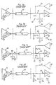
- FIG. 1b There are several ways to conventionally terminate a receiver 40 for ATE equipment and these are illustrated in Figures 1b through 1d.
- a resistive load R L is connected from input 50 of the receiver 40 to ground.
- the resistor R L equals Z O .
- R dc is the lumped resistance of the transmission line.
- R L Z O .
- One disadvantage of the prior approach of Figure 1b is that the DUT 10 must be able to supply the aforesaid value of current to the transmission line 20 when driving high. Many DUTs 10 cannot supply that amount of current.
- FIG 1c a second prior art solution for terminating a receiver 40 in an ATE system 30 is shown.
- a resistor R L which is equal to Z O is terminated on the variable drive 60.
- a second resistance R A is added at the output 80 of the DUT 10.
- the addition of resistor R A further isolates the DUT 10 from the ATE system 30. But the addition of resistor R A also means that the parasitic capacitance C pDUT becomes more important. If a correct value of R A can be found, the DUT 10 can be adequately isolated from the ATE 30.
- the problems with the prior art approach shown in Figure 1c are substantial. For some DUTs 10 there is no good value for R A .
- a resistor R L is connected in a series connection to a capacitor C L which connects the input 50 of receiver 40 to ground. Capacitor C L isolates the resistor R L from ground. Hence, the resistor R L does not DC load the DUT 10 but the capacitor C L will add to the receiver input capacitance which can limit test speed.
- the clear advantage of the approach of Figure 1d is that the resistor R L is only "present” in the circuit when a signal transition from the DUT 10 occurs at the input 50. Termination is only present when the signal at the input 50 is changing state. Hence, no DC loading.
- the design of this circuit must not interfere with the acquisition of a valid high or low signal from a wide variety of different types of DUTs 10.
- FIG. 2 illustrates a typical prior ATE system capable of interfacing with a number of DUTs 10.
- the ATE system 30 includes a set of analog multiplexors (MUX O - MUX I ) (e.g., relays) wherein each multiplexor is interconnected over a fixture and PC board 20 to a plurality of DUTs 10 (DUT A - DUT N ).
- MUX O - MUX I analog multiplexors
- each receiver termination 50 can be selectively connected by the multiplexor to a discrete DUT 10 in a set of DUTs 10. A measurement can then be taken by the receiver 40 of the signal output of the connected DUT.
- the receiver termination 210 in Figure 2 may constitute any one of the above prior art approaches fully discussed in Figure 1.
- the DUTs 10 as shown in Figure 2 may be of a number of different logic families. These different logic families will have different valid logic thresholds. For example, transistor-transistor logic (TTL) has a signal threshold of 2.0 volts and complementary metal oxide semiconductor (CMOS) has a signal threshold of 4.0 volts, both for a valid digital "1.” Furthermore, the output impedance of each logic family is also different. Hence, a need exists for each receiver to have active termination thresholds so as to adjust to the signal characteristics of the DUT being tested.
- TTL transistor-transistor logic
- CMOS complementary metal oxide semiconductor
- each receiver 40 has programmable thresholds on a per receiver basis (e.g., receiver high, receiver low, drive high, drive low). This capability is called “per-pin programmable logic threshold" in the industry. Finally, a need exists to provide distributed programmable clamps on a per-pin basis so as to provide an active termination for the receivers 40.
- U.S. Patent 3,660,675 sets forth a design for terminating a low output impedance source by adding a series termination when the device is sinking, in a diode (no series termination) when the device is sourcing.
- U.S. Patent 4,450,370 sets forth an active termination for a transmission line involving a tri-state buffer enabled by a strobe signal.
- the output of the tri-state buffer is tied through a resistive element which is used to help match the line impedance of the transmission line.
- U.S. Patent 3,832,575 sets forth a data bus transmission line termination circuit which is programmable to either a low impedance state for connection to the terminal end of the data bus or to a high impedance state for connection to an intermediate portion of the data bus.
- U.S. Patent 4,943,739 sets forth a non-reflecting transmission line termination which contains a reflection attenuator connected between the signal line and the ground line or signal line and the power line. The attenuator clamps the voltage of digital signals between ground potential and the supply line voltage.
- This invention is the most pertinent of the patents uncovered in the search to the solution of the above problem. However, this invention is not applicable to the environment of ATE systems. The signal swing of '739 must be close to V cc or to ground and, therefore, is not appropriate for use in an ATE.
- the '739 patent does not deal with the situation involving different types of DUTS - where, for example, the V cc is not always the same. Furthermore, the '739 approach requires a third line for V cc , does not provide for high currents, and does not handle the situation where V cc is less than ground.
- the present invention provides a solution to the needs set forth in Figures 1 and 2 by providing an active distributed programmable line termination for the receiver 210 which is fully programmable on a per-pin basis in an ATE system.
- the present invention provides a receiver termination which extracts energy from the output DUT signal only when the signal has passed a defined threshold level.
- Two embodiments of the present invention are set forth. In the first embodiment, the termination voltage is tied to the per-pin programmable (distributed) receiver threshold while the second embodiment allows the termination voltages to be programmed independently on a per-pin basis. Both embodiments provide per-pin programmability of the terminated voltages.
- the present invention eliminates AC loading caused when the edges of the DUT signal are going through a transition and provide only small DC loading which is present only when the signal from the DUT has exceeded the termination voltage value.
- a system for providing programmable active receiver termination in automatic test equipment wherein the automatic test equipment is capable of testing a plurality of devices under test.
- the automatic test equipment has a plurality of receivers each of which is connected to the receiver termination system of the present invention.
- the system is further connected to an analog multiplexor which selectively connects each receiver termination to one of a plurality of devices under test.
- Each of the receiver terminations is connected between one of the automatic test equipment receivers and provides a high reference voltage for clamping signals appearing on the input to the receiver at the high reference voltage tailored for the specific device under test. It also provides a low reference voltage for clamping signals appearing on the input of the receiver at a low reference voltage clamping value tailored to the device under test.
- An analog reference control is connected to each of the plurality of receiver terminations and delivers to each receiver termination high and low reference voltage clamping values tailored for each device under test connected to the receiver termination.
- a state machine controls the delivery of the high and low reference clamping voltage values to the receiver terminations.
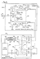
- FIG 3 the first embodiment of a receiver termination block (RTB) 300 is shown interconnected with an analog reference control 310.
- the analog reference control 310 is interconnected with a number of receiver termination blocks. With reference back to Figure 2, if there are “i" receiver terminations, then the analog reference control 310 would interface with “i" receiver termination blocks 300. This is shown in Figure 3 for RTB i .
- the analog reference control 310 outputs termination voltages as distributed per-pin programmable receiver thresholds, RHI and RLO. However, as shown in Figure 3, the termination voltages can also be tied to set reference levels, CHI and CLO. Whether programmable receiver thresholds RHI and RLO or set reference levels CHI and CLO are utilized, is dependent upon the settings of switches 320a and 320b.
- CHI and CLO signals are provided for those DUTs 10 which do not ring and which cannot drive small dc loads in the termination. Hence, CHI and CLO are outside the programming range of the receiver thresholds (i.e., CHI > RHI MAX and CLO ⁇ RLO MIN ).
- the analog reference control 310 incorporates a state machine 330, a digital to analog converter 340, an amplifier 350, and an integrated sample-and-hold circuit 360.
- the state machine 330 is interconnected over lines 332 to the digital to analog converter 340 which in turn is connected over lines 342 to the amplifier 350.
- Amplifier 350 in turn is connected over line 352 to the integrated sample-and-hold circuit 360.
- Address and enable information is delivered over lines 334 to the integrated sample-and-hold circuit 360.
- the integrated sample-and-hold circuit delivers the RLO and RHI threshold levels to the receiver termination blocks (RTB o - RTB i ).
- the analog reference control 310 provides per-pin voltages (RHI and RLO) which are used as references by the receiver termination blocks to individually configure the receiver termination block to test a particular DUT 10 so as to minimize ringing.
- Each different DUT type will have its own RHI and RLO reference voltages.
- Each analog reference voltage is separately programmable within a valid output range which in the preferred embodiment is negative 5.5 volts to positive 5.5 volts.
- the valid range of receiver levels is negative 3.5 volts to positive 5.0 volts.
- the state machine 330 cycles through all possible addresses so as to refresh each sample-and-hold 360 which in the preferred embodiment is every five microseconds with an actual switch 362 closure time of 1.6 microseconds.
- the address and enable information is delivered over lines 334 to the address decoder and switch select 364 which activates switches over lines 366.
- the state machine 330 is implemented on an ASIC which incorporates a random access memory (RAM), not shown.
- the state machine 330 conventionally operates to cycle through each address of the sample-and-hold circuit 360 which in the preferred embodiment constitutes 48 separate addresses. For each address, the state machine further provides data to the digital-to-analog converter 340. This data is delivered from the RAM lines 332, this data constitutes the necessary digital information to provide the analog threshold voltage signals amplified by amplifier 350 on lines 352.
- the state machine 330 also provides the address for the sample-and-hold circuit 360 on lines 334 and an enable signal also on lines 334 that closes the addressed switch 362 from the analog line 352 to the addressed hold capacitor 368.
- an address is delivered out from the state machine 330 on lines 334 to the address decoder and switch select 364. Simultaneously an output from the RAM internal to the state machine 330 is delivered on lines 332 to the digital-to-analog converter 340 which delivers the analog threshold value to the integrated sample-and-hold circuit 360.
- the switch 362 becomes activated and the analog value appearing on line 352 is delivered into a holding capacitor 368 for subsequent delivery as RHI or RLO to the addressed receiver termination block 300.
- 3.2 microseconds are provided for the voltage to become stable on line 352 before the enable signal on line 334 loads the value into the holding capacitor 368.
- the enable signal stays active for 1.6 microseconds allowing the hold capacitor 368 to be charged to the correct threshold value.
- An additional 200 nanoseconds of hold time is then encountered after the enable becomes inactive and then the state machine provides the address and data for the next hold capacitor.
- the digital-to-analog converter 340 and the amplifier 350 operate as follows.
- the digital-to-analog converter 340 is of the type that provides a current output.
- the digital-to-analog converter 340 converts the data being inputted on lines 332 from the state machine 330.
- the digital-to-analog converter 340 utilizes a twelve digital bit input running off of a ten volt reference.
- the output of the digital-to-analog converter 340 feeds two operational amplifiers 350, not shown.
- the first operational amplifier swings between 0 to minus ten volts depending upon the data on lines 332 and the second operational amplifier inverts the result of the first and level shifts the signal so that it runs minus 5.5 volts to plus 5.5 volts.
- the second operational amplifier inverts the result of the first and level shifts the signal so that it runs minus 5.5 volts to plus 5.5 volts.
- Only a single amplifier 350 is shown in Figure 3.
- the integrated sample-and-hold circuit 360 utilizes a decoder multiplexor 364 which selects one of the 48 sample-and-holds (based upon six binary bits).
- the enable bit from the state machine 330 closes the internal FET switch 362 from the analog input 352 from the digital-to-analog converter 340. Closure allows the internal hold capacitor 368 to be selectively charged, as discussed above.
- the voltage at the hold capacitor 368 is buffered from receiver termination blocks 300 with a low current unity gain operational amplifier 369.
- the receiver termination block 300 is connected to the fixture and PC board 20 at its input 50. This corresponds to the conventional prior art circuits of Figure 1. Likewise, the receiver termination block 300 is interconnected to the analog reference control 310 over lines RHI o and RLO o . Finally, the receiver termination block 300 delivers to the receiver outputs GTH and GTL from receiver 390.
- the diode 372a is connected through resistor R1 to the output of buffer 370a.
- the output of buffer 370a is connected to resistor R1 and through capacitor C1 to ground.
- the output of buffer 370b is connected to resistor R2 and through capacitor C2 to ground.
- the output of resistor R2 is also connected to the input of diode 372b.
- the RHI threshold signal is delivered into the high threshold comparator 380a whose output is a greater-than-high (GTH) indication.
- the RHI signal is also delivered through analog switch 320b into buffer 370a.
- RLO is delivered into the input of the comparator 380b whose output is a greater-than-low (GTL) indication.
- RLO is also delivered into the input of the buffer 370b.
- the analog switches 320 allow the termination voltage to be tied to RHI and RLO or to CHI and CLO.
- CHI and CLO are voltages which will insure that the clamps can be turned off by programming the termination voltages beyond the valid programming range of RHI and RLO.
- the analog switches 320 are digitally controlled by the control register 322 over lines 322a and 322b.
- the control register 322 is selectively loaded over lines 324 by the operator of the ATE system.
- Switches 320 are preferably DG211-a digitally controlled FET switches.
- the high current unity gain buffers 370a and 370b provide a solid high current voltage source to the RTB.
- the buffers 370a and 370b are implemented as an operational amplifier with an external current boost transistor in the feedback loop, not shown.
- Resistors R1 and R2 are current limit resistors which isolate their respective capacitors C1 and C2 from their respective high current buffer amplifiers 370a and 370b and prevent excessive currents from being drawn through the circuit if RLO is greater than RHI. This is accomplished without adding an RC time constant to RIN.
- RHI or RLO
- the capacitor C1 adjusts to the new voltage level.
- the isolation from the high current amplifier 370a and 370b keeps the voltage at the receiver input (RIN) from pulling around the voltage source when high speed pulses are stuffed into the termination 50.
- the isolation resistors R1 and R2 further protect the clamps from damage when RHI ⁇ RLO.
- the isolation resistors R1 and R2 will limit the DC load seen by the DUT when the clamps are on.
- the capacitors C1 and C2 provide charge storage and high frequency bypassing.
- the size of these capacitors is dictated by the necessary high frequency response (i.e., good high frequency bypassing) and settling time requirements when the termination voltages are changed.
- these capacitors have values in the range of 0.1 ⁇ F to 2.2 ⁇ F.
- the diodes 372a and 372b are Schottky barrier diodes in a conventionally available dual SOT-23 package. The diodes must function to turn on fast.
- the dual threshold receiver 390 is driven by the voltage at the receiver input (RIN). Dual threshold receiver 390 is essentially a voltage window receiver which uses the two comparators 380 to compare against a valid high threshold RHI and a valid low threshold RLO. Receiver outputs, as given by GTH and GTL determine the state of the receiver input RIN as follows:
- Resistor R3 has two functions. First it isolates the voltage at the receiver input RIN from electrostatic discharge and overvoltage conditions and it helps limit the current when the termination is on. Hence, the output voltage from the DUT 10 appearing at 50 will be clamped to RHI + Ioh max x (R1 + R3) + 0.3 volts high and RLO - Iol max x (R2 + R3) - 0.3 volts low .
- FIG 4 a second embodiment of the receiver termination block 300 of the present invention is set forth. Where possible, like components have been numbered with the same numerals as in Figure 3. The operation between the two embodiments is identical except as follows.
- the termination voltages represented by V cl (V clamp low) and V ch (V clamp high) are also delivered from the analog reference control 310.
- the second embodiment allows complete per-pin programmability of the termination voltage independent of the receiver threshold voltage.
- the state machine 330 and the integrated sample-and-hold circuit 360 are suitably expanded to allow for the delivery of four analog voltage values per receiver termination block.
- the second embodiment allows complete per-pin programmability of the termination voltage independent of the receiver threshold voltage. This allows additional flexibility and fine tuning at the termination voltage for optimum performance.
- the trade-offs in the second embodiment to provide this fine tuning results in the delivery of four rather than two reference voltages and the complexity of the analog reference control is greater and more costly.
- the signal positions B through H are shown in Figure 3 based upon a signal outputted from the DUT 10 indicated by A in Figure 2.
- a 74ACT00 is connected through a standard fixture onto an ATE PC board which contains a receiver with the termination as shown in embodiment one (see Figures 2 and 3) to reference probe points as given by A, B, C, D, E, F, G, and H.
- the DUT an 74ACT00, in DIP package is driven by a Hewlett Packard 80013B pulse generator at a frequency of 7.5 MHz.
- graph A shows the waveform at the DUT (refer to Figure 2 - Point A) with the clamps on.
- the vertical axis has a scale of 2 volts per grid, the timescale is 30 nsec/div. This is also the trigger for the oscilloscope - an HP 54110D digital oscilloscope.
- Graphs B1 and B2 of Figure 5 show the DUT waveform at the receiver RIN input (point B of Figure 3).
- B1 shows the case where the termination of the present invention is not present (i.e., ringing) while B2 shows the case where the termination is present.
- the ringing without termination in B1 is 1.76 volts as shown by line 504 and the ringing with termination is 0.78 volts as shown by line 506.
- the rising edge 500 does not ring as much as the falling edge 502 between the two graphs B1 and B2.
- the ringing will be much greater on the rising edge (i.e., similar to what is displayed on the falling edge of graph B1).
- diode 372 and capacitor C are not ideal. This non-ideality shows up as a finite turn-on time which allows these fast edges to overshoot slightly the first time and ring once. Note that the peak of the ring (as shown by 506 in Figure B2) never reaches the RLO threshold of 0.8 volts. If further improvement becomes necessary a faster diode and better capacitor C can be chosen to reduce the single ring and the voltage 506. This implementation was the best cost-performance trade-off. The example of Figure 5 also represents the worst performance configuration. Changing the fixture, DUTs, PC board, and grounding to DUTs PC board also improves the performance as characterized by the ringing seen at the receiver.
- graph C shows the voltage at point C of about 0.52 volts, between diode 372b and capacitor C2 of Figure 3. This is the normal voltage at point C (the RLO termination) for a reasonable ATE test frequency of 7.5 MHz. (This voltage will move somewhat as the capacitor charges and discharges at lower frequency as displayed in Figure 6, graph C.)
- graph D shows the output at the voltage source 370b of about 0.968 volts. Notice that this point is a little noisy. This noise is from circuitry switching and impinging upon the non-ideal voltage source (i.e., AC bandwidth does not equal infinity).
- the trace length on the PC board through the isolation resistor and to the filter capacitor can reach upwards of fourteen inches. Such noise can be minimized by proper routing of grounds and signals.
- graph E shows the RLO voltage of 0.96 volts as programmed into the termination circuit 300. Notice that this voltage is 200 millivolts above the peak voltage seen in graph B2.
- graphs F, G, and H show similar points on the high side of the termination.
- Graph F is the voltage of 3.92 volts between diode 372a and capacitor C1 of Figure 3. This is the voltage that sets the point where the diode 372a will turn on.
- Graph G is the voltage output (2.16 volts) of the high current buffer amplifier while graph H is the RHI voltage input of 2.16 volts to the buffer amplifier and receiver. Notice that the voltage of graph F is somewhat above the voltage of graphs G and H. This is because as the diode 372a is on more and more the capacitor tends to charge up. Therefore, at higher frequencies the termination point will tend to move away from the threshold increasing the difference in voltage between the clamp value and receiver threshold voltage. This implies that there is more noise margin and the DUT is more lightly loaded.
- graph C acts the same way - only the magnitude is smaller.
- FIG. 5 illustrates the operation of the present invention of Figure 3.
- the rising edges of the digital signal are clamped at a predetermined high voltage value (based on RHI, which, for example in Figure 5, Graph F is 3.92 volts) to minimize ringing.
- the falling edges of the digital signal are clamped at a predetermined low voltage value (based on RLO, which, for example in Figure 5, Graph C is 0.52 volts). The digital signal between these clamping values is not affected.
- the graphs of Figure 6 use the same measurement setup as Figure 5 (voltage is 2 volts per division with a time base of 50 microseconds/division). The only difference is the frequency at which the DUT is switching - now only 4.5 KHz - rather slow for an ATE but certainly possible for some cases.
- Graph A is again the DUT waveform as shown at point A of Figure 2.
- Graph B, of Figure 6, shows the DUT waveform at point B, the receiver input - RIN. Notice at this lower frequency the lessening of the load on the DUT as the capacitor charges (most noticeable on the positive going pulse).
- Graphs C and F of Figure 6 shows the capacitor C charging and discharging. Charging takes place through the diodes 372 respectively. Discharging takes place through resistors R2 and R1. There is no adverse affects on the termination circuit or the receiver input, RIN, at startup or low frequency operation.
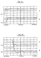
- Figure 7 shows a blowup of the ringing at the receiver input (voltage is 2 volts per division and the time base is 10 nsec/division).
- the top signal of Figures 7a-7d shows the DUT waveform at A on Figure 2 while the bottom waveform shows the waveform at part B of Figure 3.
- Figures 7a and 7b illustrate the rising and falling edges of an 74ACT00 (same setup/measurement technique as used in Figures 5 and 6) with the termination turned off (programmed to CHI and CLO)
- Figures 7c and 7d are the equivalent waveforms with the termination turned on. Notice the difference in the bottom waveforms B of 7a and 7c. There is distinctly less overshoot and lessening in the DC level achieved by the part. Likewise, the bottom waveforms of 7b and 7d can be compared. Here a dramatic decrease in ringing can be observed. Finally, note the top waveforms of the pairs 7a and 7c, 7b and 7d are not affected by the presence or absence of the termination. This implies that the DUT is fully capable of driving the small load presented by the termination.
Landscapes
- Engineering & Computer Science (AREA)
- General Engineering & Computer Science (AREA)
- Physics & Mathematics (AREA)
- General Physics & Mathematics (AREA)
- Tests Of Electronic Circuits (AREA)
- Testing Electric Properties And Detecting Electric Faults (AREA)
Applications Claiming Priority (2)
| Application Number | Priority Date | Filing Date | Title |
|---|---|---|---|
| US07/625,716 US5164663A (en) | 1990-12-05 | 1990-12-05 | Active distributed programmable line termination for in-circuit automatic test receivers |
| US625716 | 1996-03-29 |
Publications (3)
| Publication Number | Publication Date |
|---|---|
| EP0489510A2 true EP0489510A2 (fr) | 1992-06-10 |
| EP0489510A3 EP0489510A3 (en) | 1993-06-16 |
| EP0489510B1 EP0489510B1 (fr) | 1997-04-02 |
Family
ID=24507260
Family Applications (1)
| Application Number | Title | Priority Date | Filing Date |
|---|---|---|---|
| EP91310502A Expired - Lifetime EP0489510B1 (fr) | 1990-12-05 | 1991-11-14 | Termination active d'une ligne distribuée programmable pour récepteurs de test automatiques |
Country Status (4)
| Country | Link |
|---|---|
| US (1) | US5164663A (fr) |
| EP (1) | EP0489510B1 (fr) |
| JP (1) | JP3186152B2 (fr) |
| DE (1) | DE69125459T2 (fr) |
Cited By (3)
| Publication number | Priority date | Publication date | Assignee | Title |
|---|---|---|---|---|
| FR2709351A1 (fr) * | 1993-08-03 | 1995-03-03 | Schlumberger Technologies Inc | Circuits Driver pour testeur de circuits intégrés. |
| WO1999049330A1 (fr) * | 1998-03-26 | 1999-09-30 | Teradyne, Inc. | Compensation des effets du temps de propagation aller-retour dans les appareils de controle automatique |
| EP1001349A3 (fr) * | 1998-11-09 | 2002-07-03 | Alcatel USA Sourcing, L.P. | Réseau de terminaison pouvant être commandé par programme pour un bus de fond de panier à haute vitesse |
Families Citing this family (40)
| Publication number | Priority date | Publication date | Assignee | Title |
|---|---|---|---|---|
| US5408146A (en) * | 1992-01-31 | 1995-04-18 | Lsi Logic Corporation | High performance backplane driver circuit |
| US5422608A (en) * | 1992-09-23 | 1995-06-06 | Texas Instruments Incorporated | Adaptive transmission line termination |
| US5701309A (en) * | 1992-12-02 | 1997-12-23 | At&T Global Information Solutions Company | Automated test equipment digital tester expansion apparatus |
| US5463359A (en) * | 1994-03-21 | 1995-10-31 | Texas Instruments Incorporated | Impedance matching network for low output impedance devices |
| US5585741B1 (en) * | 1994-04-22 | 2000-05-02 | Unitrode Corp | Impedance emulator |
| US5682337A (en) * | 1995-04-13 | 1997-10-28 | Synopsys, Inc. | High speed three-state sampling |
| JP3469351B2 (ja) | 1995-04-17 | 2003-11-25 | 三菱電機株式会社 | リンギング防止回路、デバイスアンダーテストボード、ピンエレクトロニクスカード及び半導体装置 |
| US5530377A (en) * | 1995-07-05 | 1996-06-25 | International Business Machines Corporation | Method and apparatus for active termination of a line driver/receiver |
| US5811984A (en) * | 1995-10-05 | 1998-09-22 | The Regents Of The University Of California | Current mode I/O for digital circuits |
| US5705937A (en) * | 1996-02-23 | 1998-01-06 | Cypress Semiconductor Corporation | Apparatus for programmable dynamic termination |
| US5726583A (en) * | 1996-07-19 | 1998-03-10 | Kaplinsky; Cecil H. | Programmable dynamic line-termination circuit |
| EP1282315A3 (fr) * | 1997-03-21 | 2004-09-01 | Canal+ Technologies | Carte à puce utilisable avec un récepteur de signaux de radiodiffusion chiffres et récepteur |
| US6373260B1 (en) * | 1998-02-24 | 2002-04-16 | Agilent Technologies, Inc. | Single cable, single point, stimulus and response probing system and method |
| JP3053012B2 (ja) * | 1998-03-02 | 2000-06-19 | 日本電気株式会社 | 半導体装置の試験回路および試験方法 |
| JP3872594B2 (ja) * | 1998-05-21 | 2007-01-24 | 株式会社アドバンテスト | 半導体試験装置 |
| US6198307B1 (en) * | 1998-10-26 | 2001-03-06 | Rambus Inc. | Output driver circuit with well-controlled output impedance |
| US6408347B1 (en) | 1998-12-10 | 2002-06-18 | Cisco Technology, Inc. | Integrated multi-function adapters using standard interfaces through single a access point |
| US6175239B1 (en) * | 1998-12-29 | 2001-01-16 | Intel Corporation | Process and apparatus for determining transmission line characteristic impedance |
| US6501293B2 (en) | 1999-11-12 | 2002-12-31 | International Business Machines Corporation | Method and apparatus for programmable active termination of input/output devices |
| US6671844B1 (en) * | 2000-10-02 | 2003-12-30 | Agilent Technologies, Inc. | Memory tester tests multiple DUT's per test site |
| US6798237B1 (en) | 2001-08-29 | 2004-09-28 | Altera Corporation | On-chip impedance matching circuit |
| US6603329B1 (en) | 2001-08-29 | 2003-08-05 | Altera Corporation | Systems and methods for on-chip impedance termination |
| US6590413B1 (en) | 2001-10-03 | 2003-07-08 | Altera Corporation | Self-tracking integrated differential termination resistance |
| US6812732B1 (en) | 2001-12-04 | 2004-11-02 | Altera Corporation | Programmable parallel on-chip parallel termination impedance and impedance matching |
| US6836144B1 (en) | 2001-12-10 | 2004-12-28 | Altera Corporation | Programmable series on-chip termination impedance and impedance matching |
| US6812734B1 (en) | 2001-12-11 | 2004-11-02 | Altera Corporation | Programmable termination with DC voltage level control |
| US7109744B1 (en) | 2001-12-11 | 2006-09-19 | Altera Corporation | Programmable termination with DC voltage level control |
| KR100471544B1 (ko) * | 2002-05-30 | 2005-03-10 | 주식회사 유니테스트 | 실장과 에이티이가 통합된 반도체 소자 테스트 장치 |
| US6888369B1 (en) | 2003-07-17 | 2005-05-03 | Altera Corporation | Programmable on-chip differential termination impedance |
| US6859064B1 (en) | 2003-08-20 | 2005-02-22 | Altera Corporation | Techniques for reducing leakage current in on-chip impedance termination circuits |
| US6888370B1 (en) | 2003-08-20 | 2005-05-03 | Altera Corporation | Dynamically adjustable termination impedance control techniques |
| US7218155B1 (en) | 2005-01-20 | 2007-05-15 | Altera Corporation | Techniques for controlling on-chip termination resistance using voltage range detection |
| US7221193B1 (en) | 2005-01-20 | 2007-05-22 | Altera Corporation | On-chip termination with calibrated driver strength |
| US7333311B2 (en) * | 2005-05-27 | 2008-02-19 | Agilent Technologies, Inc. | Method and structure for AC coupled insitu ESD protection |
| US7679397B1 (en) | 2005-08-05 | 2010-03-16 | Altera Corporation | Techniques for precision biasing output driver for a calibrated on-chip termination circuit |
| US7518392B2 (en) * | 2006-08-02 | 2009-04-14 | Texas Instruments Incorporated | Systems and methods for continuity testing using a functional pattern |
| CN101846707B (zh) * | 2010-02-04 | 2012-07-18 | 艾默生网络能源有限公司 | 一种低压侧实现低电压穿越试验平台的设备及方法 |
| US9823306B2 (en) | 2016-02-11 | 2017-11-21 | Texas Instruments Incorporated | Measuring internal signals of an integrated circuit |
| WO2018022126A1 (fr) * | 2016-07-27 | 2018-02-01 | Hubbell Incorporated | Systèmes, appareils et procédés de détection de transmission entrante à deux lignes sur un bus de communication de données |
| US11448559B2 (en) * | 2018-03-30 | 2022-09-20 | Panasonic Intellectual Property Management Co., Ltd. | Capacitance detection device for detecting the capacitance of a sensor element |
Family Cites Families (13)
| Publication number | Priority date | Publication date | Assignee | Title |
|---|---|---|---|---|
| US2853630A (en) * | 1954-06-08 | 1958-09-23 | Hughes Aircraft Co | Circuits for clamping voltage levels in gating matrices |
| US3532982A (en) * | 1967-01-03 | 1970-10-06 | Tektronix Inc | Transmission line termination circuit |
| US3600634A (en) * | 1969-12-16 | 1971-08-17 | Integrated Systems Inc | Protective control circuit against transient voltages |
| US3660675A (en) * | 1970-05-05 | 1972-05-02 | Honeywell Inc | Transmission line series termination network for interconnecting high speed logic circuits |
| US3832575A (en) * | 1972-12-27 | 1974-08-27 | Ibm | Data bus transmission line termination circuit |
| US4450370A (en) * | 1979-01-31 | 1984-05-22 | Phillips Petroleum Company | Active termination for a transmission line |
| US4675551A (en) * | 1986-03-04 | 1987-06-23 | Prime Computer, Inc. | Digital logic bus termination using the input clamping Schottky diodes of a logic circuit |
| US4791312A (en) * | 1987-06-08 | 1988-12-13 | Grumman Aerospace Corporation | Programmable level shifting interface device |
| US4859877A (en) * | 1988-01-04 | 1989-08-22 | Gte Laboratories Incorporated | Bidirectional digital signal transmission system |
| US4894829A (en) * | 1988-04-21 | 1990-01-16 | Honeywell Inc. | Comprehensive design and maintenance environment for test program sets |
| US4943739A (en) * | 1988-12-19 | 1990-07-24 | Slaughter Grimes G | Non-reflecting transmission line termination |
| US4947113A (en) * | 1989-03-31 | 1990-08-07 | Hewlett-Packard Company | Driver circuit for providing pulses having clean edges |
| US4985672A (en) * | 1989-12-11 | 1991-01-15 | Advantest Corporation | Test equipment for a low current IC |
-
1990
- 1990-12-05 US US07/625,716 patent/US5164663A/en not_active Expired - Fee Related
-
1991
- 1991-11-14 EP EP91310502A patent/EP0489510B1/fr not_active Expired - Lifetime
- 1991-11-14 DE DE69125459T patent/DE69125459T2/de not_active Expired - Fee Related
- 1991-12-03 JP JP34783391A patent/JP3186152B2/ja not_active Expired - Fee Related
Cited By (4)
| Publication number | Priority date | Publication date | Assignee | Title |
|---|---|---|---|---|
| FR2709351A1 (fr) * | 1993-08-03 | 1995-03-03 | Schlumberger Technologies Inc | Circuits Driver pour testeur de circuits intégrés. |
| WO1999049330A1 (fr) * | 1998-03-26 | 1999-09-30 | Teradyne, Inc. | Compensation des effets du temps de propagation aller-retour dans les appareils de controle automatique |
| EP1001349A3 (fr) * | 1998-11-09 | 2002-07-03 | Alcatel USA Sourcing, L.P. | Réseau de terminaison pouvant être commandé par programme pour un bus de fond de panier à haute vitesse |
| US7005938B1 (en) | 1998-11-09 | 2006-02-28 | Alcatel Usa Sourcing, L.P. | Software controllable termination network for high speed backplane bus |
Also Published As
| Publication number | Publication date |
|---|---|
| JP3186152B2 (ja) | 2001-07-11 |
| EP0489510A3 (en) | 1993-06-16 |
| EP0489510B1 (fr) | 1997-04-02 |
| DE69125459D1 (de) | 1997-05-07 |
| US5164663A (en) | 1992-11-17 |
| JPH05232171A (ja) | 1993-09-07 |
| DE69125459T2 (de) | 1997-07-17 |
Similar Documents
| Publication | Publication Date | Title |
|---|---|---|
| EP0489510B1 (fr) | Termination active d'une ligne distribuée programmable pour récepteurs de test automatiques | |
| US6275023B1 (en) | Semiconductor device tester and method for testing semiconductor device | |
| EP1722247B1 (fr) | Procédé de compensation de la dégradation du signal test en raison d'un DUT défaillant | |
| US7408373B2 (en) | Device for probe card power bus voltage drop reduction | |
| US5302863A (en) | CMOS peak amplitude detector | |
| US7509227B2 (en) | High-speed digital multiplexer | |
| US5696773A (en) | Apparatus for performing logic and leakage current tests on a digital logic circuit | |
| US5642067A (en) | Variable slew rate pulse generator | |
| US6294949B1 (en) | Voltage drive circuit, voltage drive apparatus and semiconductor-device testing apparatus | |
| US6292342B1 (en) | Voltage protection circuit for semiconductor test system | |
| US5929671A (en) | Waveform generator | |
| US6621321B2 (en) | Circuit for conditioning output waveform | |
| EP1070260B1 (fr) | Agencement d'essai de courant transitoire d'un circuit cmos electronique numerique | |
| US7333311B2 (en) | Method and structure for AC coupled insitu ESD protection | |
| EP1692056A2 (fr) | Circuit de generateur pulse a amplificateur de charge | |
| JPS6081836A (ja) | 集積回路論理チップの試験装置 | |
| JP3589934B2 (ja) | 半導体集積回路試験装置 | |
| US8120380B2 (en) | Comprehensive application power tester | |
| US20260106603A1 (en) | Driving High Speed Voltage Waveforms for Current Measurements | |
| JPH04259868A (ja) | Ic試験装置 | |
| JPS63127614A (ja) | ピ−クデイテクタ回路 | |
| JP2003156528A (ja) | 半導体試験装置 | |
| JPH04172270A (ja) | Ic試験装置 |
Legal Events
| Date | Code | Title | Description |
|---|---|---|---|
| PUAI | Public reference made under article 153(3) epc to a published international application that has entered the european phase |
Free format text: ORIGINAL CODE: 0009012 |
|
| AK | Designated contracting states |
Kind code of ref document: A2 Designated state(s): DE FR GB |
|
| PUAL | Search report despatched |
Free format text: ORIGINAL CODE: 0009013 |
|
| AK | Designated contracting states |
Kind code of ref document: A3 Designated state(s): DE FR GB |
|
| 17P | Request for examination filed |
Effective date: 19931119 |
|
| 17Q | First examination report despatched |
Effective date: 19951205 |
|
| GRAG | Despatch of communication of intention to grant |
Free format text: ORIGINAL CODE: EPIDOS AGRA |
|
| GRAH | Despatch of communication of intention to grant a patent |
Free format text: ORIGINAL CODE: EPIDOS IGRA |
|
| GRAH | Despatch of communication of intention to grant a patent |
Free format text: ORIGINAL CODE: EPIDOS IGRA |
|
| GRAA | (expected) grant |
Free format text: ORIGINAL CODE: 0009210 |
|
| AK | Designated contracting states |
Kind code of ref document: B1 Designated state(s): DE FR GB |
|
| REF | Corresponds to: |
Ref document number: 69125459 Country of ref document: DE Date of ref document: 19970507 |
|
| ET | Fr: translation filed | ||
| PLBE | No opposition filed within time limit |
Free format text: ORIGINAL CODE: 0009261 |
|
| STAA | Information on the status of an ep patent application or granted ep patent |
Free format text: STATUS: NO OPPOSITION FILED WITHIN TIME LIMIT |
|
| 26N | No opposition filed | ||
| REG | Reference to a national code |
Ref country code: GB Ref legal event code: 732E |
|
| REG | Reference to a national code |
Ref country code: GB Ref legal event code: 732E |
|
| REG | Reference to a national code |
Ref country code: FR Ref legal event code: TP |
|
| REG | Reference to a national code |
Ref country code: FR Ref legal event code: TP |
|
| PGFP | Annual fee paid to national office [announced via postgrant information from national office to epo] |
Ref country code: GB Payment date: 20011018 Year of fee payment: 11 Ref country code: DE Payment date: 20011018 Year of fee payment: 11 |
|
| REG | Reference to a national code |
Ref country code: GB Ref legal event code: IF02 |
|
| PGFP | Annual fee paid to national office [announced via postgrant information from national office to epo] |
Ref country code: FR Payment date: 20021017 Year of fee payment: 12 |
|
| PG25 | Lapsed in a contracting state [announced via postgrant information from national office to epo] |
Ref country code: GB Free format text: LAPSE BECAUSE OF NON-PAYMENT OF DUE FEES Effective date: 20021114 |
|
| PG25 | Lapsed in a contracting state [announced via postgrant information from national office to epo] |
Ref country code: DE Free format text: LAPSE BECAUSE OF NON-PAYMENT OF DUE FEES Effective date: 20030603 |
|
| GBPC | Gb: european patent ceased through non-payment of renewal fee | ||
| PG25 | Lapsed in a contracting state [announced via postgrant information from national office to epo] |
Ref country code: FR Free format text: LAPSE BECAUSE OF NON-PAYMENT OF DUE FEES Effective date: 20040730 |
|
| REG | Reference to a national code |
Ref country code: FR Ref legal event code: ST |