EP0489945A1 - Dispositif de commutation pour un GTO-HF - Google Patents
Dispositif de commutation pour un GTO-HF Download PDFInfo
- Publication number
- EP0489945A1 EP0489945A1 EP90123659A EP90123659A EP0489945A1 EP 0489945 A1 EP0489945 A1 EP 0489945A1 EP 90123659 A EP90123659 A EP 90123659A EP 90123659 A EP90123659 A EP 90123659A EP 0489945 A1 EP0489945 A1 EP 0489945A1
- Authority
- EP
- European Patent Office
- Prior art keywords
- gate
- current
- gto
- anode
- semiconductor component
- Prior art date
- Legal status (The legal status is an assumption and is not a legal conclusion. Google has not performed a legal analysis and makes no representation as to the accuracy of the status listed.)
- Granted
Links
- 239000003990 capacitor Substances 0.000 abstract description 15
- 239000004065 semiconductor Substances 0.000 abstract description 12
- 238000000034 method Methods 0.000 description 9
- 230000008569 process Effects 0.000 description 9
- 230000008901 benefit Effects 0.000 description 3
- 238000011161 development Methods 0.000 description 3
- 238000010586 diagram Methods 0.000 description 3
- 230000006872 improvement Effects 0.000 description 3
- 239000004020 conductor Substances 0.000 description 2
- 238000001816 cooling Methods 0.000 description 2
- 230000006378 damage Effects 0.000 description 2
- 238000013461 design Methods 0.000 description 2
- 238000002347 injection Methods 0.000 description 2
- 239000007924 injection Substances 0.000 description 2
- 230000003071 parasitic effect Effects 0.000 description 2
- 238000011084 recovery Methods 0.000 description 2
- 230000002441 reversible effect Effects 0.000 description 2
- 239000004642 Polyimide Substances 0.000 description 1
- 230000004913 activation Effects 0.000 description 1
- 238000004458 analytical method Methods 0.000 description 1
- 238000013459 approach Methods 0.000 description 1
- 230000008859 change Effects 0.000 description 1
- 239000002800 charge carrier Substances 0.000 description 1
- 238000010276 construction Methods 0.000 description 1
- 230000002498 deadly effect Effects 0.000 description 1
- 230000003111 delayed effect Effects 0.000 description 1
- 230000001419 dependent effect Effects 0.000 description 1
- 238000007599 discharging Methods 0.000 description 1
- 238000005516 engineering process Methods 0.000 description 1
- 230000002349 favourable effect Effects 0.000 description 1
- 230000006698 induction Effects 0.000 description 1
- 230000002045 lasting effect Effects 0.000 description 1
- 231100000518 lethal Toxicity 0.000 description 1
- 230000001665 lethal effect Effects 0.000 description 1
- 230000003137 locomotive effect Effects 0.000 description 1
- 230000005923 long-lasting effect Effects 0.000 description 1
- 238000012423 maintenance Methods 0.000 description 1
- 238000004519 manufacturing process Methods 0.000 description 1
- 238000005259 measurement Methods 0.000 description 1
- 230000007246 mechanism Effects 0.000 description 1
- 229920001721 polyimide Polymers 0.000 description 1
- 230000008092 positive effect Effects 0.000 description 1
- 230000009467 reduction Effects 0.000 description 1
- 238000011144 upstream manufacturing Methods 0.000 description 1
Images

Classifications
-
- H—ELECTRICITY
- H03—ELECTRONIC CIRCUITRY
- H03K—PULSE TECHNIQUE
- H03K17/00—Electronic switching or gating, i.e. not by contact-making and –breaking
- H03K17/51—Electronic switching or gating, i.e. not by contact-making and –breaking characterised by the components used
- H03K17/56—Electronic switching or gating, i.e. not by contact-making and –breaking characterised by the components used by the use, as active elements, of semiconductor devices
- H03K17/72—Electronic switching or gating, i.e. not by contact-making and –breaking characterised by the components used by the use, as active elements, of semiconductor devices having more than two PN junctions; having more than three electrodes; having more than one electrode connected to the same conductivity region
- H03K17/73—Electronic switching or gating, i.e. not by contact-making and –breaking characterised by the components used by the use, as active elements, of semiconductor devices having more than two PN junctions; having more than three electrodes; having more than one electrode connected to the same conductivity region for DC voltages or currents
- H03K17/732—Measures for enabling turn-off
-
- H—ELECTRICITY
- H03—ELECTRONIC CIRCUITRY
- H03K—PULSE TECHNIQUE
- H03K17/00—Electronic switching or gating, i.e. not by contact-making and –breaking
- H03K17/04—Modifications for accelerating switching
- H03K17/0403—Modifications for accelerating switching in thyristor switches
-
- H—ELECTRICITY
- H03—ELECTRONIC CIRCUITRY
- H03K—PULSE TECHNIQUE
- H03K17/00—Electronic switching or gating, i.e. not by contact-making and –breaking
- H03K17/08—Modifications for protecting switching circuit against overcurrent or overvoltage
- H03K17/081—Modifications for protecting switching circuit against overcurrent or overvoltage without feedback from the output circuit to the control circuit
- H03K17/0814—Modifications for protecting switching circuit against overcurrent or overvoltage without feedback from the output circuit to the control circuit by measures taken in the output circuit
- H03K17/08144—Modifications for protecting switching circuit against overcurrent or overvoltage without feedback from the output circuit to the control circuit by measures taken in the output circuit in thyristor switches
Definitions
- the invention relates to a switching arrangement for a high-power HF-GTO, comprising a latching semiconductor component with an anode, a cathode and a gate and means for generating a gate current I G at the gate for switching off the semiconductor component.
- GTO Global System for Mobile Communications
- traction e.g. locomotives
- UPS uninterruptible power supply
- industrial drives This widespread use has taken place, although the GTO has a number of problems for the user in terms of circuitry, for example. An improvement of the GTO or its wiring is therefore of enormous economic importance.
- switchable thyristors have had to be operated with substantial wiring networks (snubbers).
- snubbers In addition to additional weight, increased volume and considerable losses, this also entails additional development and manufacturing costs.
- the development of control software is also much more complex due to the complicated mode of operation determined by the snubbers. The aim is therefore to make the snubbers smaller (smaller inductors and smaller capacitors) and to simplify them. Stray inductance and snubber diode in particular play an important role. In order to reduce overvoltages, a considerable amount of construction work has to be carried out. Recently, very special diodes have also been developed for these applications.
- the declared goal of users and manufacturers is the HF-GTO.
- this should be characterized by a significantly lower wiring effort, by low control power and low switch-off failures.
- a major obstacle is the lack of knowledge of the real causes of the switch-off failures in the GTO.
- the object of the invention is to provide a switching arrangement of the type mentioned at the outset which eliminates the problems existing in the prior art.
- the desired HF GTO should be able to be realized with the known GTO housings if possible.
- the invention provides various approaches to solving the problem. Both individually and in connection with each other, they lead to the goal. They are all based on the knowledge of the real causes for the failure of the GTOs when switching off.
- One or more of the four conditions can advantageously be met using the circuit technology described below.
- the gate unit is connected to the gate of the GTO component as inductively as possible, so that a gate circuit inductance of preferably less than 50 nH is present.
- a flat-ribbon conductor as described, for example, in published patent application EP-0,381,849 A1, is particularly suitable as the low-inductance connection.
- means for example at least one capacitance C R1 or a pulse shape network
- the gate current should in any case be greater than the tail current.
- the said means preferably comprise a capacitance C R1 , which has a voltage of at least 100 V before the GTO component is switched off. In this way, the desired gate current can be built up sufficiently quickly despite the existing gate circuit inductance. In addition, it is advisable to provide at least one further capacitance C E1 , which draws a longer-lasting holding current out of the gate after the capacitance C R1 has been discharged.
- a conventional snubber (with a capacitance C s ) will be required in order to keep the overvoltages caused by L A within the usual range.
- Means for keeping the energy stored in the inductance L A away from the parallel capacitance C p can preferably be provided, which act in the manner of a freewheel and consequently allow particularly low overvoltages and simultaneous energy return.
- the circuits for switching on and off are preferably designed analogously in terms of circuitry.
- the rate of increase dI G / dt should be greater than 200 A / ⁇ s.
- means for limiting the speed of the anode voltage rise dV A / dt during the shutdown process should preferably be provided.
- the invention is primarily directed to circuits in which the means for generating the gate current (gate unit) are arranged outside the housing of the semiconductor component. This applies to most conventional components in the preferred performance class from 1.5 kV and from 1 kA.
- latching semiconductor component encompasses 2-layer components of the type FCTh or SITh as well as 4-layer components of the type GTO or FS-GTO.
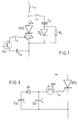
- Fig. 1 shows a circuit diagram of a conventional GTO circuit.
- the GTO component is at the center.
- a choke L A is attached to its anode to limit the dI / dt.
- the snubber comprises an inductor L s , a capacitance C s , a resistor R s and a diode D s .
- a gate unit GU is provided which discharges a capacitance C G into the gate. The gate current is delayed by an inductance L G.
- FIG. 2 shows anode voltage V A , anode current I A and gate current I G when switching off incorrectly in a known GTO circuit (FIG. 1).
- the time in ⁇ s is plotted on the abscissa (the zero point is meaningless here). On the left is the current in Ampere and the voltage in volts is plotted on the right side of the illustration.
- a gate current I G with a slew rate dI G / dt of typically 10 A / ⁇ s is forced on the gate. Over an extended period of 6 to 15 ⁇ s (depending on the size of the anode current), however, the anode current continues to flow essentially unchanged.
- the gate current I G reaches the threshold defined by the switch-off gain, which brings the GTO to switch off.
- the cathode current I K must be greater than zero until the anode current I A has dropped to the level of the gate current I G (time t 2 in FIG. 2).
- the component is in this time period (ie from t1 to t2) in an unstable and thus dangerous state:
- the GTO which is designed as a switch and not as a controller (think of the well-known equivalent circuit diagram of two coupled transistors), has to respond to this stress inevitably react with current inhomogeneities.
- the anode current I A is smaller than the gate current I G and the cathode current I K as a result is negative.
- the GTO is again in a stable condition.
- the anode voltage V A continues to rise.
- the anode current I A passes through a minimum before the tail current begins. As soon as the tail current cuts the gate current I G (time t3), the component comes into the second, but this time with certainty, lethal danger zone.
- the anode current I A begins to rise extremely steeply since the current from the snubber (the diode is flooded, the inductance L s is quite small) and is not obtained via the di / dt choke L A (FIG. 1). It is therefore a matter of switching the GTO on beyond any permissible specification (no di / dt limitation, undefined rise rate of the gate current, flooded component in the tail current range).
- the fact that the anode voltage does not immediately drop to zero immediately after t3, but only to about 300 V, indicates that only individual cells turn on (current inhomogeneity). The GTO does not survive such loads, however, it burns.
- the means for controlling the gate are to be designed such that the switch-off gain I A / I G , peak is significantly less than 3, in particular less than or equal to 2. This should result in an anode voltage rise of at least 1 kV / ⁇ s
- the switch-off process is understood to mean that period of time that begins when the threshold value is reached by the gate current (cf. switch-off gain) and ends when the tail current decays. If this second condition is met, then it is also the first one formulated above.
- a third condition which is primarily aimed at avoiding the second danger zone, is that the gate control is to be designed in such a way that the gate stream I G when switched off is at least twice as large as the tail current I Tail that occurs .
- a control in which the gate current I G has a slew rate dI G / dt leads to the realization of an HF GTO, which is sufficient to build up a gate current in the size of the maximum anode current I A, max that can be switched off within 1 ⁇ s.
- the gate current I G should therefore have a rate of increase dI G / dt of at least 1 kA / ⁇ s.
- the charge carriers in the GTO gate are sucked off so quickly that the injection from the cathode emitters is stopped immediately.
- the suction affects all GTO cells at the same time. This prevents undesired current focusing.
- a GTO must therefore be controlled much faster than before. If you control a GTO faster, however, its shutdown process is accelerated right from the start. Then it falls the slow process of reducing injection (slow "stalling") away from the cathode, and the cathodes can be turned off quickly. As a result, the anode voltage rise is no longer slow and round, but hard and fast. Then, however, the snubber diode D s and the parasitic inductance L s react with an even greater overvoltage, so that on balance there is no gain for the GTO (namely, it must continue to lead to a considerable anode voltage). So you have to reduce the gate circuit inductance to insignificance (development of a new, low-inductance housing), or you have to change the snubber.
- the snubber has to be changed in such a way that the spike voltage turns out to be smaller than before despite the increased dI / dt. This cannot be achieved by reducing the parasitic inductance L s alone, because the forward recovery of the diode D s always remains in a circle.
- special diodes are already being developed for conventional snubbers (so that larger L s can be permitted again and the structure can be simplified), no decisive progress can be achieved with the most suitable Si diodes.
- the good way is to connect at least part of the snubber capacity directly in parallel to the GTO.
- the circuit inductance then drops so far (5 - 10 nH) that the capacitor can already take on anode current noticeably before the anode voltage has passed the 100 V limit. Together with the increased gate current (faster also means lower switch-off gain), the cathode current can then go to zero in time, ie before there is much more than 100 V anode voltage. Under 100 - 200 V, however, a GTO can switch off almost any current without destruction, as already mentioned.
- Part of C s should therefore be connected in parallel to the GTO (eg 1 ⁇ F at 3 kA would depress the anode current to approx. 1/2 - 1/5 of the on value when 100 - 200 V is reached.
- the parallel connected The capacitor discharges directly into the GTO, while the plasma is still very small in normal ignition.
- GTOs would be destroyed without further precautions (exceeding the dI A / dt limit value). If the GTO is now controlled hard (fast) when igniting, its destruction by discharging the parallel capacitor can be avoided. GTOs become faster and more homogeneous when they are switched on.
- the dI A / dt is only exceeded for a very short time (namely to discharge the parallel capacitor), the associated energy and power density is relatively low (at 3 kV and 1 ⁇ F, 4.5 J would be stored, which is 450 W at 100 Hz , ie less than half of the typical switch-off losses).
- the gate circuit inductance is predetermined by the inductance that is unavoidable in conventional housing designs.
- the aim of the invention is to implement an HF GTO with conventional semiconductor components. The effort associated with the redesign of housings should be avoided.
- the capacitance C R1 is dimensioned (taking into account the actual inductance in the GTO housing) so that it unites after discharge Gate current has built up, which corresponds to the maximum anode current that can be switched off.
- the relatively long-lasting current from C E1 must be offered with a voltage that is below the avalanche of the gate-cathode path (15-25 V).
- a gate current is therefore offered which is sufficiently high and fast that the cathode current is less than zero under all circumstances. With the longer lasting low voltage can be avoided that the gate current collapses when switching and the device in the critical second zone (Fig. 2: time t3) runs.
- a pulse shape network known per se is also suitable for generating a rapidly increasing gate current which is always above the tail current. What is less important is the specific circuit design than the fulfillment of the intended function.
- a large part of the gate circuit inductance is generated in conventional circuits by the coaxial cable between the gate unit and the outer gate connection of the GTO component (FIG. 1: L G ). Of the typical 300 nH (ie L G total), only about 30 nH are in the GTO housing. According to a preferred embodiment of the invention, the gate unit is therefore connected to the gate with a ribbon conductor, as is known from EP-0,381,849 A1 (eg polyimide ribbon metallized on both sides) of the GTO component connected. In this way, gate circuit inductances L G ⁇ 50 nH can be realized without having to replace the existing housing with new one. This leads to the desired rate of increase dI G / dt ⁇ 1 kA / ⁇ s. A maximum of about 5 kA / ⁇ s can be achieved with these simple precautions.
- one advantage of the hard control is the short storage time: while in the prior art the gate current rises so slowly that up to 15 ⁇ s elapses between triggering the gate switch (MOSFET) and starting the switch-off process in the GTO, the steep rise ensures according to the invention that this delay comes to be in the range of 1 microseconds.
- the fluctuations in the storage time which is known to depend on the respective size of the anode current, are much smaller in the invention: because of the steep rise in gate current, the fluctuations can only be in the range of a few 100 ns. Overall, the switching process is more controllable.
- the gate circuit according to the invention also saves energy. A much higher gate current has to be generated, but only over a very short time. The high switch-off gain that has always been required for energy reasons is therefore becoming less important. Even in the small L G , much less energy is stored than in the prior art.
- the parallel capacitance C p enables the GTO to be safely switched off. It must be dimensioned so that the anode voltage rise dV A / dt is limited so that only part of the load current (approx. 1/2 - 1/5) flows through the GTO, when the anode voltage passes the 100 V mark. However, it should be kept so small that when it is switched on, its discharge into the GTO does not make a noticeable contribution to its losses, so as not to make GTO cooling more difficult.
- Favorable C p values for the control mentioned above are calculated according to the following rule:
- C p is thus a factor 6-20 smaller than C s today (Fig. 1). Accordingly, less energy is stored in it.
- the additional load caused by the direct discharge of C p is in the order of 10% of the total thermal load of the GTO.
- the remaining snubber circuitry (C s , D s , R s ) and / or any clamping capacitor for limiting voltage peaks due to load and leakage inductances can be dimensioned largely independently of the GTO component.
- a diode D A is preferably used in parallel with L A (dI / dt choke), or circuits such as the known undeland circuit are used, so that the energy stored in L A is not transmitted to C s . Otherwise, uneconomically high overvoltages can result. C s is therefore only used to limit the dV / dt on the GTO itself. Since enough gate current is available due to the hard control, C s can usually even be made completely zero. In other words, the conventional part of the snubber circuit (L s , C s , D s , R s ) can be omitted altogether. The problems associated with the reverse recovery of the diode D s , which were alleviated anyway by the C p according to the invention, then disappear altogether.
- L A dI / dt choke
- the invention also proposes improvements when switching on the GTO, which advantageously interact with the rest of the circuitry (see above).
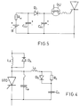
- FIG. 5 shows a preferred embodiment of the gate circuit for switching on the GTO. It realizes a hard switch-on: As with switch-off (only with reverse polarity), a rapidly increasing, strong current surge is applied to the gate.
- the circuit is advantageously similar to that required for switching off. In this way, an essentially symmetrical connection of the gate is obtained.
- a rapidly increasing current is injected into the gate of the GTO from a capacitor C R2 of high voltage (preferably ⁇ 100 V).
- a capacitor C E2 of high voltage (preferably ⁇ 100 V).
- C E2 has a low voltage (typically 15 V) compared to C R2 .
- a diode D2 separates the high voltage from the low voltage capacitor C R2 or C E2 .
- the holding current comes, for example, from the battery B indicated in the figure via the resistor R H.
- the GTO should also be able to withstand higher dI A / dt values. There is therefore a prospect of a reduction in L A (ie less energy is stored in L A ).
- the load capacity may depend on various factors, ie it will have to be type-tested from element to element.
- the invention has shown the way to implement an HF GTO.
- the wiring effort is significantly reduced and at the same time the security against fraud is increased.
- the HF-GTO can be built in particular with semiconductor components that are already commercially available.
- B - battery B - battery; C s , C G , C p , C R1 , C R2 , C E1 , C E2 - capacitance; D s , D1, D2 - diode; GU - gate unit; I A - anode current; I G - gate current; I K - cathode current: L A - di / dt choke; L s , L G - inductance; R s , R H - resistance; V A - anode voltage.
Landscapes
- Power Conversion In General (AREA)
- Thyristors (AREA)
Priority Applications (5)
| Application Number | Priority Date | Filing Date | Title |
|---|---|---|---|
| EP02011727A EP1248368A3 (fr) | 1990-12-08 | 1990-12-08 | Dispositif de commutation pour un GTO-HF |
| EP90123659A EP0489945B1 (fr) | 1990-12-08 | 1990-12-08 | Dispositif de commutation pour un GTO-HF |
| DE59010931T DE59010931D1 (de) | 1990-12-08 | 1990-12-08 | Schaltanordnung für einen HF-GTO |
| US07/800,239 US5237225A (en) | 1990-12-08 | 1991-11-29 | Switching arrangement for an rf gto |
| JP32339491A JP3244735B2 (ja) | 1990-12-08 | 1991-12-06 | Rf gto用スィッチング装置 |
Applications Claiming Priority (1)
| Application Number | Priority Date | Filing Date | Title |
|---|---|---|---|
| EP90123659A EP0489945B1 (fr) | 1990-12-08 | 1990-12-08 | Dispositif de commutation pour un GTO-HF |
Related Child Applications (2)
| Application Number | Title | Priority Date | Filing Date |
|---|---|---|---|
| EP02011727A Division-Into EP1248368A3 (fr) | 1990-12-08 | 1990-12-08 | Dispositif de commutation pour un GTO-HF |
| EP02011727A Division EP1248368A3 (fr) | 1990-12-08 | 1990-12-08 | Dispositif de commutation pour un GTO-HF |
Publications (2)
| Publication Number | Publication Date |
|---|---|
| EP0489945A1 true EP0489945A1 (fr) | 1992-06-17 |
| EP0489945B1 EP0489945B1 (fr) | 2003-01-29 |
Family
ID=8204818
Family Applications (2)
| Application Number | Title | Priority Date | Filing Date |
|---|---|---|---|
| EP02011727A Ceased EP1248368A3 (fr) | 1990-12-08 | 1990-12-08 | Dispositif de commutation pour un GTO-HF |
| EP90123659A Expired - Lifetime EP0489945B1 (fr) | 1990-12-08 | 1990-12-08 | Dispositif de commutation pour un GTO-HF |
Family Applications Before (1)
| Application Number | Title | Priority Date | Filing Date |
|---|---|---|---|
| EP02011727A Ceased EP1248368A3 (fr) | 1990-12-08 | 1990-12-08 | Dispositif de commutation pour un GTO-HF |
Country Status (4)
| Country | Link |
|---|---|
| US (1) | US5237225A (fr) |
| EP (2) | EP1248368A3 (fr) |
| JP (1) | JP3244735B2 (fr) |
| DE (1) | DE59010931D1 (fr) |
Cited By (9)
| Publication number | Priority date | Publication date | Assignee | Title |
|---|---|---|---|---|
| US5345096A (en) * | 1992-08-15 | 1994-09-06 | Abb Research Ltd. | Turn-off high-power semiconductor component with low inductive housing |
| DE19523095A1 (de) * | 1995-06-26 | 1997-01-02 | Abb Management Ag | Stromrichterschaltungsanordnung |
| EP0776083A2 (fr) | 1995-11-23 | 1997-05-28 | Asea Brown Boveri Ag | Convertisseur de puissance |
| EP0785627A3 (fr) * | 1996-01-17 | 1999-06-16 | Mitsubishi Denki Kabushiki Kaisha | Appareil de commutation à semi-conducteurs et procédé de commande d'un élément commutateur semi-conducteur |
| US6072200A (en) * | 1997-03-05 | 2000-06-06 | Asea Brown Boveri Ag | Gate unit for a hard-driven GTO |
| US6130524A (en) * | 1997-07-31 | 2000-10-10 | Asea Brown Boveri Ag | Method and apparatus for generating and injecting reactive power into an electrical AC power grid system using an inverter |
| US6191640B1 (en) | 1997-07-24 | 2001-02-20 | Asea Brown Boveri Ag | Method and device for driving a turn-off thyristor |
| WO2015179195A1 (fr) * | 2014-05-20 | 2015-11-26 | General Electric Company | Unité de commande de grille et procédé de commande d'une unité de commande de grille |
| EP3051646A1 (fr) * | 2015-01-30 | 2016-08-03 | General Electric Company | Système d'alimentation en courant continu |
Families Citing this family (7)
| Publication number | Priority date | Publication date | Assignee | Title |
|---|---|---|---|---|
| DE4136181A1 (de) * | 1991-11-02 | 1993-05-06 | Asea Brown Boveri Ag, Baden, Aargau, Ch | Gto-thyristorschaltung |
| DE4229771A1 (de) * | 1992-09-05 | 1994-03-10 | Asea Brown Boveri | Rückspeisefähige Beschaltung für Zweipunkt- und Dreipunkt-Wechselrichter sowie Verfahren zur Rückspeisung der Beschaltungsenergie |
| DE59407007D1 (de) * | 1993-12-23 | 1998-11-05 | Asea Brown Boveri | Umrichteranordnung mit niederinduktivem Kommutierungskreis |
| JP4059330B2 (ja) * | 1998-06-11 | 2008-03-12 | 有限会社 エルメック | Gtoサイリスタのゲートドライブ装置 |
| US6426666B1 (en) * | 1999-11-10 | 2002-07-30 | Virginia Tech Intellectual Properties, Inc. | Diode-assisted gate turn-off thyristor |
| EP3364533B1 (fr) * | 2017-02-17 | 2019-09-18 | General Electric Technology GmbH | Perfectionnement apportés ou se rapportant aux circuit d'attaque de grille pour tube à décharge |
| CN107835002B (zh) * | 2017-09-20 | 2024-03-12 | 同方威视技术股份有限公司 | 固态脉冲调制器中的保护电路、振荡补偿电路和供电电路 |
Citations (3)
| Publication number | Priority date | Publication date | Assignee | Title |
|---|---|---|---|---|
| FR2580127A1 (fr) * | 1985-04-05 | 1986-10-10 | Mitsubishi Electric Corp | |
| EP0228226A2 (fr) * | 1985-12-16 | 1987-07-08 | Kabushiki Kaisha Toshiba | Circuit d'extinction pour un thyristor à blocage par la gâchette |
| EP0320784A2 (fr) * | 1987-12-12 | 1989-06-21 | Asea Brown Boveri Aktiengesellschaft | Procédés et dispositifs pour la commande d'un thyristor blocable |
Family Cites Families (15)
| Publication number | Priority date | Publication date | Assignee | Title |
|---|---|---|---|---|
| JPS5932011B2 (ja) * | 1978-06-19 | 1984-08-06 | 三菱電機株式会社 | サイリスタの消孤装置 |
| JPS5568735A (en) * | 1978-11-20 | 1980-05-23 | Toshiba Corp | Gate circuit of gto |
| FR2481545A1 (fr) * | 1980-04-29 | 1981-10-30 | Thomson Csf | Interrupteur statique haute tension, applicable notamment a un generateur haute tension commutable |
| JPS5752231A (en) * | 1980-09-12 | 1982-03-27 | Hitachi Ltd | Turn-off system of semiconductor |
| JPS6053488B2 (ja) * | 1980-12-29 | 1985-11-26 | 株式会社日立製作所 | ゲ−トタ−ンオフサイリスタのゲ−ト回路 |
| JPS5917862A (ja) * | 1982-06-25 | 1984-01-30 | Hitachi Ltd | ゲ−トタ−ンオフサイリスタの並列接続体 |
| US4733146A (en) * | 1984-11-09 | 1988-03-22 | Reliance Electric Company | Energy recovery system for cyclic drives |
| JPS6291018A (ja) * | 1985-10-16 | 1987-04-25 | Fuji Electric Co Ltd | ゲ−トタ−ンオフサイリスタのゲ−ト駆動回路 |
| US4805081A (en) * | 1987-06-29 | 1989-02-14 | Spellman High Voltage Electronics Corp. | Multi-mode control systems for high-frequency resonant inverters |
| EP0335169A1 (fr) * | 1988-03-28 | 1989-10-04 | Siemens Aktiengesellschaft | Dispositif de commutation symétrique sans porte et de faible puissance reactive appliqué aux éléments de commutation semi-conducteurs d'un onduleur |
| DE58905048D1 (de) * | 1988-12-14 | 1993-09-02 | Asea Brown Boveri | Verfahren zur steuerung eines dreiphasigen wechselrichters. |
| EP0381849A1 (fr) * | 1989-02-07 | 1990-08-16 | Asea Brown Boveri Ag | Circuit semi-conducteur de puissance rapide |
| CA2013492C (fr) * | 1989-03-31 | 1995-07-25 | Shigeru Tanaka | Convertisseur d'alimentation multitension et multifrequence |
| US4965709A (en) * | 1989-09-25 | 1990-10-23 | General Electric Company | Switching converter with pseudo-resonant DC link |
| US5051603A (en) * | 1990-08-14 | 1991-09-24 | General Electric Company | Method and apparatus for matching turn-off times of parallel connected semiconductor switching devices |
-
1990
- 1990-12-08 DE DE59010931T patent/DE59010931D1/de not_active Expired - Lifetime
- 1990-12-08 EP EP02011727A patent/EP1248368A3/fr not_active Ceased
- 1990-12-08 EP EP90123659A patent/EP0489945B1/fr not_active Expired - Lifetime
-
1991
- 1991-11-29 US US07/800,239 patent/US5237225A/en not_active Expired - Lifetime
- 1991-12-06 JP JP32339491A patent/JP3244735B2/ja not_active Expired - Lifetime
Patent Citations (3)
| Publication number | Priority date | Publication date | Assignee | Title |
|---|---|---|---|---|
| FR2580127A1 (fr) * | 1985-04-05 | 1986-10-10 | Mitsubishi Electric Corp | |
| EP0228226A2 (fr) * | 1985-12-16 | 1987-07-08 | Kabushiki Kaisha Toshiba | Circuit d'extinction pour un thyristor à blocage par la gâchette |
| EP0320784A2 (fr) * | 1987-12-12 | 1989-06-21 | Asea Brown Boveri Aktiengesellschaft | Procédés et dispositifs pour la commande d'un thyristor blocable |
Non-Patent Citations (2)
| Title |
|---|
| BROWN BOVERI REVIEW, Band 73, Nr. 9, September 1986, Seiten 519-525, Baden, CH; D. EISELE et al.: "Two new GTO modules for drive applications" * |
| CONFERENCE RECORD INDUSTRY APPLICATIONS SOCIETY, IEEE-IAS-1985 ANNUAL MEETING, Toronto, 6. - 11. Oktober 1985, Seitens 955-959; A.P. CONNOLLY et al.: "Application of GTO thyristor modules" * |
Cited By (16)
| Publication number | Priority date | Publication date | Assignee | Title |
|---|---|---|---|---|
| US5345096A (en) * | 1992-08-15 | 1994-09-06 | Abb Research Ltd. | Turn-off high-power semiconductor component with low inductive housing |
| DE19523095A1 (de) * | 1995-06-26 | 1997-01-02 | Abb Management Ag | Stromrichterschaltungsanordnung |
| US5731967A (en) * | 1995-06-26 | 1998-03-24 | Asea Brown Boveri Ag | Converter circuit arrangement with minimal snubber |
| EP0751612A3 (fr) * | 1995-06-26 | 1998-04-22 | Asea Brown Boveri Ag | Convertisseur de puissance |
| CN1076901C (zh) * | 1995-11-23 | 2001-12-26 | 亚瑞亚·勃朗勃威力有限公司 | 逆变器电路装置 |
| EP0776083A2 (fr) | 1995-11-23 | 1997-05-28 | Asea Brown Boveri Ag | Convertisseur de puissance |
| US5768114A (en) * | 1995-11-23 | 1998-06-16 | Asea Brown Boveri Ag | Converter circuit arrangement |
| EP0776083A3 (fr) * | 1995-11-23 | 1998-12-02 | Asea Brown Boveri Ag | Convertisseur de puissance |
| EP0785627A3 (fr) * | 1996-01-17 | 1999-06-16 | Mitsubishi Denki Kabushiki Kaisha | Appareil de commutation à semi-conducteurs et procédé de commande d'un élément commutateur semi-conducteur |
| US6072200A (en) * | 1997-03-05 | 2000-06-06 | Asea Brown Boveri Ag | Gate unit for a hard-driven GTO |
| US6191640B1 (en) | 1997-07-24 | 2001-02-20 | Asea Brown Boveri Ag | Method and device for driving a turn-off thyristor |
| US6130524A (en) * | 1997-07-31 | 2000-10-10 | Asea Brown Boveri Ag | Method and apparatus for generating and injecting reactive power into an electrical AC power grid system using an inverter |
| WO2015179195A1 (fr) * | 2014-05-20 | 2015-11-26 | General Electric Company | Unité de commande de grille et procédé de commande d'une unité de commande de grille |
| US9401708B2 (en) | 2014-05-20 | 2016-07-26 | General Electric Company | Gate drive unit and method for controlling a gate drive unit |
| EP3051646A1 (fr) * | 2015-01-30 | 2016-08-03 | General Electric Company | Système d'alimentation en courant continu |
| US9853451B2 (en) | 2015-01-30 | 2017-12-26 | General Electric Company | Direct current power system |
Also Published As
| Publication number | Publication date |
|---|---|
| DE59010931D1 (de) | 2003-03-06 |
| JPH04275056A (ja) | 1992-09-30 |
| EP0489945B1 (fr) | 2003-01-29 |
| EP1248368A3 (fr) | 2003-02-19 |
| JP3244735B2 (ja) | 2002-01-07 |
| EP1248368A2 (fr) | 2002-10-09 |
| US5237225A (en) | 1993-08-17 |
Similar Documents
| Publication | Publication Date | Title |
|---|---|---|
| EP0489945B1 (fr) | Dispositif de commutation pour un GTO-HF | |
| DE69628514T2 (de) | Leistungspulsgenerator mit energierückgewinnung | |
| DE60015052T2 (de) | Halbleiter-Leistungswandlungsvorrichtung | |
| DE69404498T2 (de) | Kraftstoffeinspritz-Regelvorrichtung für eine Brennkraftmaschine | |
| DE3702680A1 (de) | Verfahren und schaltung zur ansteuerung von elektromagnetischen verbrauchern | |
| DE2058091A1 (de) | Gleichstromregelschaltung | |
| DE4218662C2 (de) | Dreipunkt-Wechselrichter | |
| DE3403619C2 (fr) | ||
| EP3151405A1 (fr) | Circuit d'équilibrage des tensions aux bornes des condensateurs d'un circuit intermédiaire à courant continu | |
| DE1513868A1 (de) | Zuendschaltung fuer steuerbare Gleichrichter | |
| DE2927058C2 (de) | Steuereinrichtung für eine Zündspule | |
| DE2506021A1 (de) | Ueberspannungs-schutzschaltung fuer hochleistungsthyristoren | |
| DE69029150T2 (de) | Entladungsangeregte Impulslaservorrichtung | |
| DE1238067B (de) | Schaltung zur Erzeugung steiler Impulse aus einer Gleichspannungsquelle | |
| EP0565667B1 (fr) | Circuit a thyristors gto | |
| EP0167734A1 (fr) | Circuit de protection pour un thyristor | |
| EP1524768B1 (fr) | Procédé et dispositif servant à commander un thyristor blocable | |
| EP3207612A1 (fr) | Interrupteur de puissance de courant continu comprenant une unité de courant impulsionnel ainsi que procédé servant à commuter un courant continu | |
| DE2724741A1 (de) | Schutzbeschaltung fuer jeweils ein stromrichterventil | |
| EP1071210A2 (fr) | Montage de circuit | |
| EP0134433B1 (fr) | Circuit de commande pour appareils à courant impulsionnel | |
| DE10042292A1 (de) | Excimer-Laser | |
| DE69809632T2 (de) | Schneller, als Anordnung elementarer Thyristoren realisierter Schalter mit hoher Gleichspannungs- und Gleichstromfestigkeit | |
| DE2443892C2 (de) | Schaltungsanordnung zur Herabsetzung der auftretenden Verlustleistung beim Abschalten einer wenigstens einen Halbleiterschalter und eine Induktanz enthaltenden Reihenschaltung | |
| EP0509118A1 (fr) | Montage en série d'éléments semi-conducteurs de puissance blocables par la gâchette |
Legal Events
| Date | Code | Title | Description |
|---|---|---|---|
| PUAI | Public reference made under article 153(3) epc to a published international application that has entered the european phase |
Free format text: ORIGINAL CODE: 0009012 |
|
| AK | Designated contracting states |
Kind code of ref document: A1 Designated state(s): AT BE CH DE DK ES FR GB GR IT LI LU NL SE |
|
| RBV | Designated contracting states (corrected) |
Designated state(s): BE CH DE FR GB IT LI NL |
|
| 17P | Request for examination filed |
Effective date: 19921113 |
|
| 17Q | First examination report despatched |
Effective date: 19951227 |
|
| RAP1 | Party data changed (applicant data changed or rights of an application transferred) |
Owner name: ABB (SCHWEIZ) AG |
|
| RAP1 | Party data changed (applicant data changed or rights of an application transferred) |
Owner name: ABB SEMICONDUCTORS AG |
|
| GRAG | Despatch of communication of intention to grant |
Free format text: ORIGINAL CODE: EPIDOS AGRA |
|
| RAP1 | Party data changed (applicant data changed or rights of an application transferred) |
Owner name: ABB SCHWEIZ AG |
|
| GRAG | Despatch of communication of intention to grant |
Free format text: ORIGINAL CODE: EPIDOS AGRA |
|
| GRAH | Despatch of communication of intention to grant a patent |
Free format text: ORIGINAL CODE: EPIDOS IGRA |
|
| GRAH | Despatch of communication of intention to grant a patent |
Free format text: ORIGINAL CODE: EPIDOS IGRA |
|
| GRAA | (expected) grant |
Free format text: ORIGINAL CODE: 0009210 |
|
| AK | Designated contracting states |
Designated state(s): BE CH DE FR GB IT LI NL |
|
| PG25 | Lapsed in a contracting state [announced via postgrant information from national office to epo] |
Ref country code: NL Free format text: LAPSE BECAUSE OF FAILURE TO SUBMIT A TRANSLATION OF THE DESCRIPTION OR TO PAY THE FEE WITHIN THE PRESCRIBED TIME-LIMIT Effective date: 20030129 Ref country code: IT Free format text: LAPSE BECAUSE OF FAILURE TO SUBMIT A TRANSLATION OF THE DESCRIPTION OR TO PAY THE FEE WITHIN THE PRE;WARNING: LAPSES OF ITALIAN PATENTS WITH EFFECTIVE DATE BEFORE 2007 MAY HAVE OCCURRED AT ANY TIME BEFORE 2007. THE CORRECT EFFECTIVE DATE MAY BE DIFFERENT FROM THE ONE RECORDED.SCRIBED TIME-LIMIT Effective date: 20030129 |
|
| REG | Reference to a national code |
Ref country code: GB Ref legal event code: FG4D Free format text: NOT ENGLISH |
|
| REG | Reference to a national code |
Ref country code: CH Ref legal event code: EP |
|
| REF | Corresponds to: |
Ref document number: 59010931 Country of ref document: DE Date of ref document: 20030306 Kind code of ref document: P |
|
| GBT | Gb: translation of ep patent filed (gb section 77(6)(a)/1977) | ||
| NLV1 | Nl: lapsed or annulled due to failure to fulfill the requirements of art. 29p and 29m of the patents act | ||
| ET | Fr: translation filed | ||
| PLBE | No opposition filed within time limit |
Free format text: ORIGINAL CODE: 0009261 |
|
| STAA | Information on the status of an ep patent application or granted ep patent |
Free format text: STATUS: NO OPPOSITION FILED WITHIN TIME LIMIT |
|
| PG25 | Lapsed in a contracting state [announced via postgrant information from national office to epo] |
Ref country code: BE Free format text: LAPSE BECAUSE OF NON-PAYMENT OF DUE FEES Effective date: 20031231 |
|
| 26N | No opposition filed |
Effective date: 20031030 |
|
| BERE | Be: lapsed |
Owner name: *ABB SCHWEIZ A.G. Effective date: 20031231 |
|
| PGFP | Annual fee paid to national office [announced via postgrant information from national office to epo] |
Ref country code: CH Payment date: 20091224 Year of fee payment: 20 |
|
| PGFP | Annual fee paid to national office [announced via postgrant information from national office to epo] |
Ref country code: GB Payment date: 20091218 Year of fee payment: 20 Ref country code: FR Payment date: 20100108 Year of fee payment: 20 |
|
| PGFP | Annual fee paid to national office [announced via postgrant information from national office to epo] |
Ref country code: DE Payment date: 20091222 Year of fee payment: 20 |
|
| REG | Reference to a national code |
Ref country code: CH Ref legal event code: PL |
|
| REG | Reference to a national code |
Ref country code: GB Ref legal event code: PE20 Expiry date: 20101207 |
|
| PG25 | Lapsed in a contracting state [announced via postgrant information from national office to epo] |
Ref country code: GB Free format text: LAPSE BECAUSE OF EXPIRATION OF PROTECTION Effective date: 20101207 |
|
| PG25 | Lapsed in a contracting state [announced via postgrant information from national office to epo] |
Ref country code: DE Free format text: LAPSE BECAUSE OF EXPIRATION OF PROTECTION Effective date: 20101208 |