EP0490639B1 - Source d'énergie à interrupteur - Google Patents
Source d'énergie à interrupteur Download PDFInfo
- Publication number
- EP0490639B1 EP0490639B1 EP91311476A EP91311476A EP0490639B1 EP 0490639 B1 EP0490639 B1 EP 0490639B1 EP 91311476 A EP91311476 A EP 91311476A EP 91311476 A EP91311476 A EP 91311476A EP 0490639 B1 EP0490639 B1 EP 0490639B1
- Authority
- EP
- European Patent Office
- Prior art keywords
- voltage
- switch
- main
- capacitor
- main switch
- Prior art date
- Legal status (The legal status is an assumption and is not a legal conclusion. Google has not performed a legal analysis and makes no representation as to the accuracy of the status listed.)
- Expired - Lifetime
Links
- 239000003990 capacitor Substances 0.000 claims description 31
- 238000004804 winding Methods 0.000 claims description 17
- 238000003079 width control Methods 0.000 claims description 7
- 230000004044 response Effects 0.000 claims description 3
- 241001481828 Glyptocephalus cynoglossus Species 0.000 description 4
- 230000003071 parasitic effect Effects 0.000 description 4
- 238000010586 diagram Methods 0.000 description 3
- 230000008859 change Effects 0.000 description 2
- 238000010276 construction Methods 0.000 description 2
- 230000007704 transition Effects 0.000 description 2
- 230000007423 decrease Effects 0.000 description 1
- 230000000593 degrading effect Effects 0.000 description 1
- 238000004146 energy storage Methods 0.000 description 1
- 238000005516 engineering process Methods 0.000 description 1
- 230000005669 field effect Effects 0.000 description 1
- 230000001939 inductive effect Effects 0.000 description 1
- 238000009413 insulation Methods 0.000 description 1
- 238000004519 manufacturing process Methods 0.000 description 1
- 230000004048 modification Effects 0.000 description 1
- 238000012986 modification Methods 0.000 description 1
Images


Classifications
-
- H—ELECTRICITY
- H02—GENERATION; CONVERSION OR DISTRIBUTION OF ELECTRIC POWER
- H02M—APPARATUS FOR CONVERSION BETWEEN AC AND AC, BETWEEN AC AND DC, OR BETWEEN DC AND DC, AND FOR USE WITH MAINS OR SIMILAR POWER SUPPLY SYSTEMS; CONVERSION OF DC OR AC INPUT POWER INTO SURGE OUTPUT POWER; CONTROL OR REGULATION THEREOF
- H02M1/00—Details of apparatus for conversion
- H02M1/32—Means for protecting converters other than automatic disconnection
- H02M1/34—Snubber circuits
-
- H—ELECTRICITY
- H02—GENERATION; CONVERSION OR DISTRIBUTION OF ELECTRIC POWER
- H02M—APPARATUS FOR CONVERSION BETWEEN AC AND AC, BETWEEN AC AND DC, OR BETWEEN DC AND DC, AND FOR USE WITH MAINS OR SIMILAR POWER SUPPLY SYSTEMS; CONVERSION OF DC OR AC INPUT POWER INTO SURGE OUTPUT POWER; CONTROL OR REGULATION THEREOF
- H02M3/00—Conversion of DC power input into DC power output
- H02M3/01—Resonant DC/DC converters
-
- H—ELECTRICITY
- H02—GENERATION; CONVERSION OR DISTRIBUTION OF ELECTRIC POWER
- H02M—APPARATUS FOR CONVERSION BETWEEN AC AND AC, BETWEEN AC AND DC, OR BETWEEN DC AND DC, AND FOR USE WITH MAINS OR SIMILAR POWER SUPPLY SYSTEMS; CONVERSION OF DC OR AC INPUT POWER INTO SURGE OUTPUT POWER; CONTROL OR REGULATION THEREOF
- H02M3/00—Conversion of DC power input into DC power output
- H02M3/22—Conversion of DC power input into DC power output with intermediate conversion into AC
- H02M3/24—Conversion of DC power input into DC power output with intermediate conversion into AC by static converters
- H02M3/28—Conversion of DC power input into DC power output with intermediate conversion into AC by static converters using discharge tubes with control electrode or semiconductor devices with control electrode to produce the intermediate AC
- H02M3/325—Conversion of DC power input into DC power output with intermediate conversion into AC by static converters using discharge tubes with control electrode or semiconductor devices with control electrode to produce the intermediate AC using devices of a triode or a transistor type requiring continuous application of a control signal
- H02M3/335—Conversion of DC power input into DC power output with intermediate conversion into AC by static converters using discharge tubes with control electrode or semiconductor devices with control electrode to produce the intermediate AC using devices of a triode or a transistor type requiring continuous application of a control signal using semiconductor devices only
- H02M3/33569—Conversion of DC power input into DC power output with intermediate conversion into AC by static converters using discharge tubes with control electrode or semiconductor devices with control electrode to produce the intermediate AC using devices of a triode or a transistor type requiring continuous application of a control signal using semiconductor devices only having several active switching elements
-
- H—ELECTRICITY
- H02—GENERATION; CONVERSION OR DISTRIBUTION OF ELECTRIC POWER
- H02M—APPARATUS FOR CONVERSION BETWEEN AC AND AC, BETWEEN AC AND DC, OR BETWEEN DC AND DC, AND FOR USE WITH MAINS OR SIMILAR POWER SUPPLY SYSTEMS; CONVERSION OF DC OR AC INPUT POWER INTO SURGE OUTPUT POWER; CONTROL OR REGULATION THEREOF
- H02M1/00—Details of apparatus for conversion
- H02M1/32—Means for protecting converters other than automatic disconnection
- H02M1/34—Snubber circuits
- H02M1/342—Active non-dissipative snubbers
-
- Y—GENERAL TAGGING OF NEW TECHNOLOGICAL DEVELOPMENTS; GENERAL TAGGING OF CROSS-SECTIONAL TECHNOLOGIES SPANNING OVER SEVERAL SECTIONS OF THE IPC; TECHNICAL SUBJECTS COVERED BY FORMER USPC CROSS-REFERENCE ART COLLECTIONS [XRACs] AND DIGESTS
- Y02—TECHNOLOGIES OR APPLICATIONS FOR MITIGATION OR ADAPTATION AGAINST CLIMATE CHANGE
- Y02B—CLIMATE CHANGE MITIGATION TECHNOLOGIES RELATED TO BUILDINGS, e.g. HOUSING, HOUSE APPLIANCES OR RELATED END-USER APPLICATIONS
- Y02B70/00—Technologies for an efficient end-user side electric power management and consumption
- Y02B70/10—Technologies improving the efficiency by using switched-mode power supplies [SMPS], i.e. efficient power electronics conversion e.g. power factor correction or reduction of losses in power supplies or efficient standby modes
Definitions
- the present invention relates to a resonant type switching power source capable of implementing zero-voltage switching on the basis of the resonance between an inductor and a capacitor and, more particularly, to a partial voltage resonant converter incorporated in such a switching power source.
- a resonant type switching power source which can be controlled by a fixed frequency is studied.
- This type of switching power source has a partial voltage resonant converter which partially oscillates only on the turn-on and turn-off of the switches.
- a resonant converter of this kind promotes high frequency operations by reducing switching losses, allows parts which are not strictly resistive to high voltages to be used due to the voltage clamping characteristic, and frees the fixed frequency control from considerations which traditional voltage resonant converters should give to frequency control.
- a specific construction of the partial voltage resonant converter is disclosed in, for example, "Electronic Technologies", Nikkan Kogyo Shimbun, March 1990, pp. 30-37.
- the problem with the conventional partial voltage resonant converter is that the inductor for realizing zero-voltage switching is constituted by a main transformer with windings, resulting in a complicated and expensive transformer.
- Another problem is that a main switch and an auxiliary switch cannot have their potentials matched due to the particular circuit arrangement, i. e. , without resorting to an exclusive transformer for driving the auxiliary switch, further increasing the cost.
- a switching power source of the present invention comprises a main transformer, a main switch connected to the primary winding side of the main transformer, a pulse width control circuit for generating a control signal to vary the turn-on time of the main switch until the output voltage of the secondary winding side of the main transformer being fed back reaches a predetermined value, a capacitor connected in parallel with the main switch, an inductor connected with the capacitor at the junction of the capacitor and primary winding side of the main transformer, an auxiliary switch for selectively opening or closing a parallel connection of the inductor and capacitor in response to the control signal, a first diode connected in series with the main switch and rendered non-conductive when a voltage lower than zero voltage is applied to the first diode, a second diode connected in series with the auxiliary switch and rendered non-conductive when a voltage lower than zero voltage is applied to the second diode, and a control circuit for delaying the control signal to be applied from the pulse width control circuit to the main switch until the potential on the junction has been determined to be zero.
- the partial voltage resonant converter is basically implemented as a separately excited converter using a forward converter.
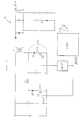
- the converter has a main switch S1, an auxiliary switch S2, a transformer T consisting of a primary winding Nr, a clamp winding Nc, an auxiliary winding Na and a secondary winding Ns, a rectifying circuit R connected to the secondary side of the transformer T, parasitic diodes D1 and D2, a clamp diode D3, a capacitor Cr for resonance, a clamp capacitor Cc, a pulse width modulation circuit PWM, a delay circuit DELAY, and a pulse transformer PT.
- FIG. 2 A reference will also be made to FIG. 2 for describing the operation of the conventional resonant converter under the heads of Modes 1-6.
- the conventional capacitor for resonance has the auxiliary winding Na in the transformer and reversely excites the transformer T by the voltage stored in the clamp capacitor Cc and the auxiliary switch S2 to thereby lower the voltage of the main switch S1 to zero, i. e. , to realize zero-voltage switching.
- the transformer T implementing the inductor is complicated in construction since it has four windings Nr, Nc, Na and Ns, as discussed earlier.
- the pulse transformer PT has to be connected to the auxiliary switch S2 since the main switch and the auxiliary switch S2 cannot have the potentials thereof matched due to the particular circuit arrangement, increasing the production cost.
- a partial voltage resonant converter embodying the present invention includes a main transformer T.
- a main switch S1 is inserted in the primary side of the main transformer T.
- a pulse width control circuit PWM generates a control signal for varying the duration of the on-state of the main witch S1 until the output voltage of the secondary side of the main transformer T being fed back reaches a predetermined value.
- a capacitor for resonance Cr is connected in parallel with the main switch S1.
- An inductor Lr for resonance is connected with the capacitor Cr at the junction of the capacitor Cr and the primary side of the main transformer T.
- An auxiliary switch S2 selectively opens or closes a parallel connection of the inductor Lr and capacitor Cr in response to the above-mentioned control signal.
- a diode D1 is connected in series with the main switch S1 and turned off when a voltage lowr than zero voltage is applied to the switch S1.
- a diode D2 is connected in series with the auxiliary switch S2 and turned off when a voltage lower than zero voltage is applied to the switch S2.
- a zero voltage sensing circuit ZVS and a flip-flop FF constitute a control circuit for delaying the control signal to be fed from the pulse width control circuit PWM to the main switch S1, until it detects the drop of the potential on the above-mentioned junction to zero.
- the operation of the embodiment will be described with reference to FIG. 4.
- the auxiliary switch S2 turns on at a time t0, the voltage across the resonant capacitor Cr sequentially decreases due to the resonance between the inductor Lr and the capacitor Cr.
- the zero voltage sensing circuit ZVS senses zero voltage and then sends a signal to the flip-flop FF to turn on the main switch S1.
- the main switch S1 should only be turned on while a negative voltage is applied (t1-t3), since the diode D1 is connected serially to the main witch S1.
- the gap between the times t0 and t1 is a constant substantially determined by the inductor Lr and dapacitor Cr for resonance, allows the zero voltage sensing circuit ZVS and flip-flop FF to be replaced with a delay circuit which sets up a predetermined delay only when the drive pulse goes high.
- This kind of delay circuit is shown as an alternative embodiment in FIG. 5.
- This time gap should preferably be as short as possible since the pulse width is uncontrollable throughout such a time gap.
- the main switch S1 While the main switch S1 is in an on-state (t1-t4), a current having a rectangular waveform flows through the main switch S1.
- the auxiliary switch S2 may be turned off any time during the period of time t2-4, i. e.
- the auxiliary resonance switching circuit is provided with a full-wave configuration. Then, when a negative current flows through the resonant inductor Lr, the exiting energy accumulated in the inductor Lr while the main switch S1 is in an on-state is consumed by the switches S1 and S2 during the period of time t3-t4, degrading the efficiency.
- the embodiment uses a half-wave configuration by connecting the diode D2 in series with the switch S2.
- FIG. 5 shows an alternative embodiment of the present invention in which a delay circuit DELAY is substituted for the zero voltage sensing circuit ZVS and flip-flop FF, as mentioned earlier. Specifically, the delay circuit DELAY sets up a predetermined or fixed delay only when the drive pulse goes high.
- the present invention provides a switching power source having a main switch and an auxiliary switch serving as a zero-voltage switch and a zero-current switch, respectively, and thereby achieves various advantages, as enumerated below.
Landscapes
- Engineering & Computer Science (AREA)
- Power Engineering (AREA)
- Dc-Dc Converters (AREA)
Claims (3)
- Source d'énergie à commutation comprenant :- un transformateur principal;- un commutateur principal connecté au côté enroulement primaire du transformateur principal;- un circuit de commande en largeur d'impulsions pour produire un signal de commande afin de faire varier le temps de mise à l'état conducteur dudit commutateur principal jusqu'à ce que la tension de sortie du côté enroulement secondaire dudit transformateur principal qui est réappliquée atteigne une valeur prédéterminée;- un condensateur monté en parallèle avec ledit commutateur principal;- un inducteur relié audit condensateur à la jonction dudit condensateur et dudit côté enroulement primaire dudit transformateur principal;- un commutateur auxiliaire pour ouvrir ou fermer sélectivement la connexion parallèle dudit inducteur et dudit condensateur en réponse audit signal de commande;- une première diode connectée en série audit commutateur principal et rendue non conductrice lorsqu'une tension inférieure à zéro volt est appliquée à ladite première diode;- une seconde diode connectée en série audit commutateur auxiliaire et rendue non conductrice lorsqu'une tension inférieure à zéro volt est appliquée à ladite seconde diode; et- un moyen de commande pour retarder ledit signal de commande devant être appliqué par ledit circuit de commande en largeur d'impulsions audit commutateur principal jusqu'à ce qu'il y ait détermination du fait que le potentiel à ladite jonction est zéro.
- Source d'énergie à commutation selon la revendication 1, dans lequel ledit moyen de commande comprend un circuit de détection de tension zéro et une bascule.
- Source d'énergie à commutation selon la revendication 1, dans lequel ledit moyen de commande comprend un circuit à retard pour retarder ledit signal de commande devant être appliqué audit commutateur principal suivant une période de temps prédéterminée par rapport audit signal de commande devant être appliqué audit commutateur auxiliaire.
Applications Claiming Priority (2)
| Application Number | Priority Date | Filing Date | Title |
|---|---|---|---|
| JP2409977A JP2961897B2 (ja) | 1990-12-10 | 1990-12-10 | スイッチング電源装置 |
| JP409977/90 | 1990-12-10 |
Publications (3)
| Publication Number | Publication Date |
|---|---|
| EP0490639A2 EP0490639A2 (fr) | 1992-06-17 |
| EP0490639A3 EP0490639A3 (en) | 1993-03-24 |
| EP0490639B1 true EP0490639B1 (fr) | 1995-06-28 |
Family
ID=18519220
Family Applications (1)
| Application Number | Title | Priority Date | Filing Date |
|---|---|---|---|
| EP91311476A Expired - Lifetime EP0490639B1 (fr) | 1990-12-10 | 1991-12-10 | Source d'énergie à interrupteur |
Country Status (6)
| Country | Link |
|---|---|
| US (1) | US5267133A (fr) |
| EP (1) | EP0490639B1 (fr) |
| JP (1) | JP2961897B2 (fr) |
| AU (1) | AU641829B2 (fr) |
| CA (1) | CA2057310C (fr) |
| DE (1) | DE69110843T2 (fr) |
Families Citing this family (36)
| Publication number | Priority date | Publication date | Assignee | Title |
|---|---|---|---|---|
| DE4328458B4 (de) * | 1992-08-25 | 2005-09-22 | Matsushita Electric Industrial Co., Ltd., Kadoma | Schalt-Spannungsversorgung |
| KR100219314B1 (ko) * | 1992-09-25 | 1999-09-01 | 무라따 미치히로 | 공진형 전원 회로 |
| US5363289A (en) * | 1992-12-15 | 1994-11-08 | At&T Bell Laboratories | Control apparatus for limiting voltage on a core reset capacitor |
| US5434768A (en) * | 1993-02-12 | 1995-07-18 | Rompower | Fixed frequency converter switching at zero voltage |
| KR100326344B1 (ko) * | 1993-03-17 | 2002-10-11 | 내셔널 세미콘덕터 코포레이션 | 스위칭레귤레이터용주파수편이회로 |
| GB9309088D0 (en) * | 1993-05-01 | 1993-06-16 | Farnell Power Limited | Feedback control loop circuits |
| US5461302A (en) * | 1993-11-30 | 1995-10-24 | At&T Corp. | Modulated snubber driver for active snubber network |
| JP3287086B2 (ja) * | 1993-12-17 | 2002-05-27 | 株式会社ニプロン | スイッチングレギュレータ |
| US5506764A (en) * | 1994-01-31 | 1996-04-09 | Astec International, Ltd. | Electrical power converter with step-gapped transformer |
| US5559685A (en) * | 1994-10-12 | 1996-09-24 | Electronic Power Conditioning, Inc. | Voltage clamped parallel resonant converter with controllable duty cycle |
| FR2738418B1 (fr) * | 1995-09-01 | 1997-11-21 | Lacme | Dispositif electrique a transformateur dont le primaire est alimente sous controle d'un hacheur |
| SG63667A1 (en) * | 1995-10-02 | 1999-03-30 | Thomson Consumer Electronics | Tuned switch-mode power supply with current mode control |
| US5875103A (en) * | 1995-12-22 | 1999-02-23 | Electronic Measurements, Inc. | Full range soft-switching DC-DC converter |
| TW349287B (en) * | 1996-09-12 | 1999-01-01 | Thomson Consumer Electronics | A forward converter with an inductor coupled to a transformer winding |
| DE19641299C2 (de) * | 1996-10-07 | 2000-08-03 | Siemens Ag | Getaktete Stromversorgung von Schaltnetzteilen |
| US5835361A (en) * | 1997-04-16 | 1998-11-10 | Thomson Consumer Electronics, Inc. | Switch-mode power supply with over-current protection |
| CA2220747A1 (fr) * | 1997-11-10 | 1999-05-10 | Praveen Kumar Jain | Convertisseurs c.c.-c.c. |
| DE19801499C2 (de) * | 1998-01-16 | 2000-05-18 | Siemens Ag | Getaktete Stromversorgung |
| US6205037B1 (en) * | 1999-12-21 | 2001-03-20 | Thomson Licensing S.A. | Overload protection for a switch mode power supply |
| US6069803A (en) * | 1999-02-12 | 2000-05-30 | Astec International Limited | Offset resonance zero volt switching flyback converter |
| JP2001224170A (ja) * | 2000-02-09 | 2001-08-17 | Sony Corp | スイッチング電源回路 |
| US6466460B1 (en) | 2001-08-24 | 2002-10-15 | Northrop Grumman Corporation | High efficiency, low voltage to high voltage power converter |
| US6650551B1 (en) * | 2002-06-06 | 2003-11-18 | Astec International Limited | ZVS/ZVT resonant choke with voltage clamp winding |
| CN103066855B (zh) | 2013-01-15 | 2015-06-24 | 昂宝电子(上海)有限公司 | 用于电源变换系统中的零电压开关的系统和方法 |
| CA2526713C (fr) * | 2003-05-23 | 2012-10-02 | Auckland Uniservices Limited | Convertisseur auto-oscillant a regulation de frequence |
| GB0327002D0 (en) | 2003-11-20 | 2003-12-24 | Rolls Royce Plc | A method of manufacturing a fibre reinforced metal matrix composite article |
| US7006364B2 (en) * | 2004-03-15 | 2006-02-28 | Delta Electronics, Inc. | Driving circuit for DC/DC converter |
| EP1635462A1 (fr) * | 2004-09-13 | 2006-03-15 | Peter Laurence Hutchins | Convertisseur de puissance à découpage à haute efficacité |
| US7940536B2 (en) * | 2006-05-30 | 2011-05-10 | International Rectifier Corporation | Flyback converter with improved synchronous rectification |
| BRPI0721576A2 (pt) | 2007-05-25 | 2013-01-15 | Thomson Licensing | suprimento de energia elÉtrica |
| CN101577493B (zh) * | 2008-05-07 | 2011-06-15 | 群康科技(深圳)有限公司 | 电源电路 |
| TWI474601B (zh) * | 2009-10-08 | 2015-02-21 | Acbel Polytech Inc | High conversion efficiency of the pulse mode resonant power converter |
| KR101350575B1 (ko) * | 2012-12-20 | 2014-01-13 | 삼성전기주식회사 | 플라이백 컨버터 |
| CN106160709B (zh) | 2016-07-29 | 2019-08-13 | 昂宝电子(上海)有限公司 | 减少功率变换系统中的开关损耗的系统和方法 |
| US11088624B2 (en) * | 2019-07-30 | 2021-08-10 | Power Forest Technology Corporation | Voltage conversion apparatus for implementing zero-voltage switching based on recovering leakage inductance energy |
| KR20230098137A (ko) * | 2020-08-20 | 2023-07-03 | 조지아 테크 리서치 코포레이션 | 소프트-스위칭 전류원 컨버터 제어를 위한 시스템 및 방법 |
Family Cites Families (10)
| Publication number | Priority date | Publication date | Assignee | Title |
|---|---|---|---|---|
| DE3007597C2 (de) * | 1980-02-28 | 1982-04-15 | Siemens Ag, 1000 Berlin Und 8000 Muenchen | Schutzbeschaltungsanordnung für Halbleiterschalter |
| ATE37519T1 (de) * | 1985-06-27 | 1988-10-15 | Haagexport Bv | Verschlussvorrichtung fuer saecke. |
| US4785387A (en) * | 1986-04-28 | 1988-11-15 | Virginia Tech Intellectual Properties, Inc. | Resonant converters with secondary-side resonance |
| US4857822A (en) * | 1987-09-23 | 1989-08-15 | Virginia Tech Intellectual Properties, Inc. | Zero-voltage-switched multi-resonant converters including the buck and forward type |
| US4931716A (en) * | 1989-05-05 | 1990-06-05 | Milan Jovanovic | Constant frequency zero-voltage-switching multi-resonant converter |
| US4975821A (en) * | 1989-10-10 | 1990-12-04 | Lethellier Patrice R | High frequency switched mode resonant commutation power supply |
| US5066900A (en) * | 1989-11-14 | 1991-11-19 | Computer Products, Inc. | Dc/dc converter switching at zero voltage |
| US4959764A (en) * | 1989-11-14 | 1990-09-25 | Computer Products, Inc. | DC/DC converter switching at zero voltage |
| FR2658674B1 (fr) * | 1990-02-20 | 1992-05-07 | Europ Agence Spatiale | Convertisseur continu-continu a commutation a tension nulle. |
| US5172309A (en) * | 1991-08-07 | 1992-12-15 | General Electric Company | Auxiliary quasi-resonant dc link converter |
-
1990
- 1990-12-10 JP JP2409977A patent/JP2961897B2/ja not_active Expired - Lifetime
-
1991
- 1991-12-09 CA CA002057310A patent/CA2057310C/fr not_active Expired - Fee Related
- 1991-12-09 AU AU88961/91A patent/AU641829B2/en not_active Ceased
- 1991-12-10 EP EP91311476A patent/EP0490639B1/fr not_active Expired - Lifetime
- 1991-12-10 US US07/804,584 patent/US5267133A/en not_active Expired - Fee Related
- 1991-12-10 DE DE69110843T patent/DE69110843T2/de not_active Expired - Fee Related
Also Published As
| Publication number | Publication date |
|---|---|
| JP2961897B2 (ja) | 1999-10-12 |
| JPH04210775A (ja) | 1992-07-31 |
| CA2057310C (fr) | 1997-10-28 |
| EP0490639A2 (fr) | 1992-06-17 |
| DE69110843D1 (de) | 1995-08-03 |
| AU8896191A (en) | 1992-06-11 |
| US5267133A (en) | 1993-11-30 |
| AU641829B2 (en) | 1993-09-30 |
| DE69110843T2 (de) | 1996-03-14 |
| EP0490639A3 (en) | 1993-03-24 |
| CA2057310A1 (fr) | 1992-06-11 |
Similar Documents
| Publication | Publication Date | Title |
|---|---|---|
| EP0490639B1 (fr) | Source d'énergie à interrupteur | |
| US6005782A (en) | Flyback converter with soft switching using auxiliary switch and resonant circuit | |
| US4785387A (en) | Resonant converters with secondary-side resonance | |
| US5636114A (en) | Lossless snubber circuit for use in power converters | |
| US6061252A (en) | Switching power supply device | |
| US5490052A (en) | Switching power supply | |
| US4443839A (en) | Single ended, separately driven, resonant DC-DC converter | |
| US5991171A (en) | DC-to-DC converters | |
| US6198260B1 (en) | Zero voltage switching active reset power converters | |
| US5521807A (en) | DC-To-DC converter with secondary flyback core reset | |
| US6452814B1 (en) | Zero voltage switching cells for power converters | |
| KR100517552B1 (ko) | 스위칭 전원 장치 | |
| US5434768A (en) | Fixed frequency converter switching at zero voltage | |
| EP0508664B1 (fr) | Convertisseur continu-continu | |
| US5459650A (en) | Power supply circuit | |
| EP1130753B1 (fr) | Appareil d'alimentation de puissance à découpage | |
| US5418703A (en) | DC-DC converter with reset control for enhanced zero-volt switching | |
| US4007413A (en) | Converter utilizing leakage inductance to control energy flow and improve signal waveforms | |
| US5847941A (en) | Switching power supply system and process | |
| US5412555A (en) | Self-oscillating DC-DC Converter with zero voltage switching | |
| EP0518300B1 (fr) | Circuit d'alimentation en courant électrique | |
| JP3475892B2 (ja) | スイッチング電源装置 | |
| US4455596A (en) | Flyback-forward boost switchmode converter | |
| US6072702A (en) | Ringing choke converter | |
| EP0534379A2 (fr) | Circuit d'alimentation de puissance |
Legal Events
| Date | Code | Title | Description |
|---|---|---|---|
| PUAI | Public reference made under article 153(3) epc to a published international application that has entered the european phase |
Free format text: ORIGINAL CODE: 0009012 |
|
| 17P | Request for examination filed |
Effective date: 19920110 |
|
| AK | Designated contracting states |
Kind code of ref document: A2 Designated state(s): DE FR GB |
|
| PUAL | Search report despatched |
Free format text: ORIGINAL CODE: 0009013 |
|
| AK | Designated contracting states |
Kind code of ref document: A3 Designated state(s): DE FR GB |
|
| 17Q | First examination report despatched |
Effective date: 19941102 |
|
| GRAA | (expected) grant |
Free format text: ORIGINAL CODE: 0009210 |
|
| AK | Designated contracting states |
Kind code of ref document: B1 Designated state(s): DE FR GB |
|
| ET | Fr: translation filed | ||
| REF | Corresponds to: |
Ref document number: 69110843 Country of ref document: DE Date of ref document: 19950803 |
|
| PLBE | No opposition filed within time limit |
Free format text: ORIGINAL CODE: 0009261 |
|
| STAA | Information on the status of an ep patent application or granted ep patent |
Free format text: STATUS: NO OPPOSITION FILED WITHIN TIME LIMIT |
|
| 26N | No opposition filed | ||
| PGFP | Annual fee paid to national office [announced via postgrant information from national office to epo] |
Ref country code: GB Payment date: 20011212 Year of fee payment: 11 Ref country code: FR Payment date: 20011212 Year of fee payment: 11 |
|
| REG | Reference to a national code |
Ref country code: GB Ref legal event code: IF02 |
|
| PGFP | Annual fee paid to national office [announced via postgrant information from national office to epo] |
Ref country code: DE Payment date: 20020109 Year of fee payment: 11 |
|
| PG25 | Lapsed in a contracting state [announced via postgrant information from national office to epo] |
Ref country code: GB Free format text: LAPSE BECAUSE OF NON-PAYMENT OF DUE FEES Effective date: 20021210 |
|
| PG25 | Lapsed in a contracting state [announced via postgrant information from national office to epo] |
Ref country code: DE Free format text: LAPSE BECAUSE OF NON-PAYMENT OF DUE FEES Effective date: 20030701 |
|
| GBPC | Gb: european patent ceased through non-payment of renewal fee | ||
| PG25 | Lapsed in a contracting state [announced via postgrant information from national office to epo] |
Ref country code: FR Free format text: LAPSE BECAUSE OF NON-PAYMENT OF DUE FEES Effective date: 20030901 |
|
| REG | Reference to a national code |
Ref country code: FR Ref legal event code: ST |