EP0492962A2 - Methode und Apparat zur Herstellung kapazitiver Structuren und Laminat für deren Herstellung - Google Patents
Methode und Apparat zur Herstellung kapazitiver Structuren und Laminat für deren Herstellung Download PDFInfo
- Publication number
- EP0492962A2 EP0492962A2 EP91311754A EP91311754A EP0492962A2 EP 0492962 A2 EP0492962 A2 EP 0492962A2 EP 91311754 A EP91311754 A EP 91311754A EP 91311754 A EP91311754 A EP 91311754A EP 0492962 A2 EP0492962 A2 EP 0492962A2
- Authority
- EP
- European Patent Office
- Prior art keywords
- web
- laminate
- carrier tape
- webs
- metallized
- Prior art date
- Legal status (The legal status is an assumption and is not a legal conclusion. Google has not performed a legal analysis and makes no representation as to the accuracy of the status listed.)
- Ceased
Links
Images

Classifications
-
- H—ELECTRICITY
- H01—ELECTRIC ELEMENTS
- H01G—CAPACITORS; CAPACITORS, RECTIFIERS, DETECTORS, SWITCHING DEVICES, LIGHT-SENSITIVE OR TEMPERATURE-SENSITIVE DEVICES OF THE ELECTROLYTIC TYPE
- H01G4/00—Fixed capacitors; Processes of their manufacture
- H01G4/30—Stacked capacitors
-
- H—ELECTRICITY
- H01—ELECTRIC ELEMENTS
- H01G—CAPACITORS; CAPACITORS, RECTIFIERS, DETECTORS, SWITCHING DEVICES, LIGHT-SENSITIVE OR TEMPERATURE-SENSITIVE DEVICES OF THE ELECTROLYTIC TYPE
- H01G4/00—Fixed capacitors; Processes of their manufacture
- H01G4/002—Details
- H01G4/018—Dielectrics
- H01G4/06—Solid dielectrics
- H01G4/14—Organic dielectrics
- H01G4/18—Organic dielectrics of synthetic material, e.g. derivatives of cellulose
-
- H—ELECTRICITY
- H01—ELECTRIC ELEMENTS
- H01G—CAPACITORS; CAPACITORS, RECTIFIERS, DETECTORS, SWITCHING DEVICES, LIGHT-SENSITIVE OR TEMPERATURE-SENSITIVE DEVICES OF THE ELECTROLYTIC TYPE
- H01G13/00—Apparatus specially adapted for manufacturing capacitors; Processes specially adapted for manufacturing capacitors not provided for in groups H01G4/00 - H01G11/00
-
- H—ELECTRICITY
- H01—ELECTRIC ELEMENTS
- H01G—CAPACITORS; CAPACITORS, RECTIFIERS, DETECTORS, SWITCHING DEVICES, LIGHT-SENSITIVE OR TEMPERATURE-SENSITIVE DEVICES OF THE ELECTROLYTIC TYPE
- H01G4/00—Fixed capacitors; Processes of their manufacture
- H01G4/30—Stacked capacitors
- H01G4/308—Stacked capacitors made by transfer techniques
-
- Y—GENERAL TAGGING OF NEW TECHNOLOGICAL DEVELOPMENTS; GENERAL TAGGING OF CROSS-SECTIONAL TECHNOLOGIES SPANNING OVER SEVERAL SECTIONS OF THE IPC; TECHNICAL SUBJECTS COVERED BY FORMER USPC CROSS-REFERENCE ART COLLECTIONS [XRACs] AND DIGESTS
- Y10—TECHNICAL SUBJECTS COVERED BY FORMER USPC
- Y10T—TECHNICAL SUBJECTS COVERED BY FORMER US CLASSIFICATION
- Y10T29/00—Metal working
- Y10T29/43—Electric condenser making
- Y10T29/435—Solid dielectric type
Definitions
- This invention pertains to an improved method for making capacitive structures of a type comprising interleaved webs of metallized, dielectric film, among other elements, wherein each web has a metallized layer and an opposite, dielectric layer.
- This invention pertains also to an improved apparatus for making such structures. The improved method and the improved apparatus have particular utility if the dielectric layer of each web is ultra thin.
- This invention pertains further to a novel laminate useful in making such structures.
- Capacitive structures of the type noted above and methods for their manufacture are exemplified in Rayburn U.S. Patent No. 4,462,062, Rayburn U.S. Patent No. 4,531,268, Rayburn et al. U.S. Patent No. 4,533,813, and Rayburn U.S. Patent No. 4,849,853.
- the metallized layer of each web has narrow, longitudinal, laser-scribed, demetallized lanes.
- Miniature capacitors made from capacitive structures of the aforenoted type are available commercially from ITW-Paktron (a unit of Illinois Tool Works Inc.) of Lynchburg, Virginia, under its ANGSTOR trademark.
- capacitive structures of the type noted above comprise interleaved webs of relatively thick, metallized, dielectric film, such as poly(ethylene terephthalate) film, which can be ordinarily handled in manufacturing methods exemplified in the aforenoted patents without undue risk of damaging such film.
- capacitive structures of the aforenoted type may be made from interleaved webs of metallized, ultra thin, poly(ethylene terephthalate) film. Ultra thin film presents serious problems in manufacturing capacitive structures, since it tends to be easily damaged.
- Yoshii et al. U.S. Patent No. 4,756,064 discloses a manufacturing method employing metallized, ultra thin, poly(ethylene terephthalate) film having a thickness of from about 0.2 ⁇ m to about 2.0 ⁇ m to make a capacitive structure.
- Such film is provided in a laminated structure, in which one layer of the metallized film adheres separably to a thicker, propylene copolymer, support film. Separate coils of the laminated structure are unwound from two unwinders. The laminated structure unwound from each unwinder is passed to a pair of nip rollers where the laminated structure is separated into the metallized film and the support film. The metallized films are superposed and are wound into a coil. The support films are rewound by two winders.
- the Yoshii et al. patent refers to a five-layer structure including two ultra thin, metal-deposited films (see column 4, lines 42 through 51) and indicates that a capacitor element can be fabricated only by coiling the two films. Such patent, however, does not disclose any details of fabricating a capacitor element from the two films.
- This invention provides a method and an apparatus for making capacitive structures from interleaved webs of metallized, dielectric film, which may be ultra thin, poly(ethylene terephthalate) or PET film, wherein each web has a metallized layer and an opposite, dielectric layer.
- metallized, dielectric film which may be ultra thin, poly(ethylene terephthalate) or PET film, wherein each web has a metallized layer and an opposite, dielectric layer.
- such film may be poly(phenylene sulfide) or PPS film or may be poly(ethylene naphthalate) or PEN film.
- the dielectric layer of each web is a relatively thin layer of poly(ethylene terephthalate) film and a carrier tape is used, which may be a relatively thick layer of poly(ethylene terephthalate) film.
- the carrier tape may be a relatively thick layer of any other polymeric film having suitable properties, such as a propylene copolymer film disclosed in Yoshii et al. U.S. Patent No. 4,756,064.
- the first web adheres peelably to the carrier tape at the dielectric layer of the first web and the second web adheres peelably to the carrier tape at the dielectric layer of the second web.
- a carrier tape facilitates handling of two relatively thin webs of dielectric film, such as the ultra thin film disclosed in the Yoshii et al. patent, in the improved method of this invention.
- the carrier tape can be optionally omitted if a laminate is used that is comprised of two relatively thick webs of metallized, dielectric film, such as PET, PPS, or PPN film having a thickness in a range from about 0.5 ⁇ m to about 8.0 ⁇ m.
- Such relatively thick webs of metallized PET, PPS, or PPN film tend to be self-supporting and have sufficient tear resistance to permit their use without a carrier tape in the improved method of this invention.
- one coil of the interleaved webs is made from a laminate of indeterminate length.
- the laminate comprises a carrier tape with two opposite surfaces, a first web of the metallized film adhering peelably to the carrier tape, and a second web of the metallized film adhering peelably to the carrier tape.
- the webs adhere respectively to the opposite surfaces of the carrier tape.
- two coils of the interleaved webs are made from two laminates of indeterminate lengths.
- Each of the laminates is similar to the laminate employed in the first mode.
- the second web is peeled from the carrier tape and is wound into a coil in such manner that the metallized layer of the second web faces in a given radial direction.
- the carrier tape and the first web adhering peelably to the carrier tape are twisted, by one half-twist, after the second web has been peeled from the carrier tape.
- the first web is wound onto the second web, along with the carrier tape having the first web adhering peelably thereto, in such manner that the metallized layer of the first web faces in the same radial direction.
- the carrier tape is peeled from the first web.
- the second web is slitted into a selected number of first ribbons before the second web is wound into the coil and the first web is slitted into the selected number of second ribbons before the first web is wound onto the second web.
- the coil is divided into the selected number of coil segments, in each of which one of the first ribbons and one of the second ribbons are interleaved.
- the first mode may comprise removal of selected portions of the metallized layers of the webs, before either web is peeled from the carrier tape, in such manner that each web has the selected number of narrow, longitudinal, demetallized lanes, which are arranged in such manner that each ribbon has one of the demetallized lanes dividing the metallized layer of such ribbon into a major portion and a minor portion.
- the webs having the demetallized lanes may be wound into the coil in such manner that the first ribbons are offset axially from the second ribbons.
- the major portion of the metallized layer of each second ribbon overlies the major portion of the metallized layer of one of the first ribbons.
- Removal of selected portions of the metallized layers of the webs can be effected by applying optical energy from a laser to the metallized layer of a selected one of the webs along longitudinal lanes, in such manner that optical energy in beams from the laser removes selected portions of the metallized layer of the selected web, passes through the selected web, through the carrier tape, and through the remaining web, to the metallized layer of the remaining web, and vaporizes selected portions of the metallized layer of the remaining web.
- the first web may be heat-tacked to the second web after the first web is wound onto the second web, in each turn of the coil. Also, if the dielectric layer of the first web adheres peelably to the carrier tape, the first web may be heat-tacked to the second web, through the carrier tape, before the carrier tape is peeled from the first tape.
- the carrier tape can be optionally omitted in some instances. If the carrier tape is omitted, the first mode for carrying out this invention is simplified accordingly.
- two coils of the interleaved webs are made, namely a first coil and a second coil.
- the second web of a first laminate is peeled from the carrier tape thereof and the second web of a second laminate is peeled from its carrier tape.
- the second web from the first laminate and the first web from the second laminate, along with the carrier tape having the first web from the second laminate adhering peelably thereto, are wound into the first coil and the carrier tape is peeled from the first web from the second laminate, in such manner that the first web from the second laminate is wound onto the second web from the first laminate.
- the metallized layers of the webs wound into the first coil face in a common radial direction. Also, the webs wound into the first coil are interleaved to form the first coil.
- the second web from the second laminate and the first web from the first laminate, along with the carrier tape having the first web from the first laminate adhering peelably thereto, are wound into the second coil and the carrier tape is peeled from the first web from the first laminate, in such manner that the first web from the first laminate is wound onto the second web from the second laminate.
- the metallized layers of the webs wound into the second coil face in a common radial direction.
- the webs wound into the second coil are interleaved to form the second coil.
- each of the first webs is slitted into a selected number of first ribbons before the first webs are wound into the respective coils and each of the second webs is slitted into the selected number of second ribbons before the second webs are wound into the respective coils.
- the second mode may comprise removal of selected portions of the metallized layers of the webs of each laminate, before either web is peeled from the carrier tape of either laminate, in such manner that each web from each laminate has the selected number of narrow, longitudinal, demetallized lanes, which are arranged in such manner that each ribbon from each web from each of the laminates has one of the demetallized lanes dividing the metallized layer of such ribbon into a major portion and a minor portion.
- removal of selected portions of the metallized layer of each web in the second mode may be effected by applying optical energy in a manner discussed above in a context of the first mode.
- heat-tacking of the first web of such coil to the second web of such coil may be effected, possibly through the carrier tape having the first web of such coil adhering peelably thereto, in a manner discussed above in a context of the first mode.
- the carrier tape can be optionally omitted in some instances. If the tape is omitted, the second mode for carrying out this invention is simplified accordingly.
- the improved apparatus provided by this invention comprises various mechanisms for providing the various functions noted above. Such apparatus is provided in two preferred embodiments, each corresponding functionally to one of the preferred modes noted above.
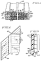
- Figure 1 is a greatly enlarged, fragmentary, cross-sectional view of a capacitive structure made by either of two disclosed modes for carrying out this invention.
- Figure 2 on a smaller scale compared to Figure 1, is a fragmentary, perspective view of a representative laminate employed by this invention.
- the laminate as shown, has a relatively thick, dielectric, carrier tape and two webs of relatively thin, metallized, dielectric film, each having laser-scribed, demetallized lanes. One of the webs is shown as being peeled from the carrier tape.
- Figure 3 on an larger scale compared to Figures 1 and 2, is a cross-sectional view of such a laminate before optical energy from a laser is applied, as and where indicated by arrows, so as to provide the demetallized lanes.
- the webs are shown as being peeled from the carrier tape.
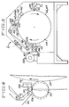
- Figure 4 on a smaller scale compared to each of Figures 1, 2, and 3, is a diagrammatic view of certain rollers and a razor blade, as used in handling the laminate.
- Figure 5 on a smaller scale compared to Figure 4, is a diagrammatic view of a preferred system for making a capacitive structure by a first mode for carrying out this invention.
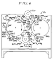
- Figure 6 on a similar scale compared to Figure 4, is a diagrammatic view of a preferred system for making a capacitive structure by a second mode for carrying out this invention.
- Figure 7 which is analogous to Figure 2, is a fragmentary, perspective view of an alternative laminate employed by this invention.
- the laminate as shown, has two webs of relatively thick, metallized, dielectric film without a carrier tape therebetween. One of the webs is shown as being peeled from the other web.
- Figure 8 which is analogous to Figure 3, is a cross-sectional view of such a laminate without a carrier tape before optical energy is applied, as and where indicated by arrows, so as to provide the demetallized lanes.
- One of the webs is shown as being beeled from the other web.
- a capacitive structure 10 comprises a group of interleaved ribbons 12 of metallized, ultra thin, dielectric film, preferably poly(ethylene terephthalate) film having a thickness of about 0.2 ⁇ m to about 2.0 ⁇ m, as described in Yoshii et al. U.S. Patent No. 4,756,064.
- such film may be poly(phenylene sulfide) film or poly(ethylene naphthalate) film, as discussed above.
- Each ribbon 12 comprises a dielectric layer 14 of the ultra thin, dielectric film and a metallized layer 16, such as an aluminized layer, which covers one surface of the dielectric layer 14, except for narrow, longitudinal, demetallized lanes 18 dividing the metallized layer 16 into a relatively wide or major portion 20 and a relatively narrow or minor portion 22.
- the metallized layer 16 is an aluminized layer having a thickness of about 300 angstroms (30nm).
- the ribbons 12 are arranged in an alternating pattern, in a first group and a second group.
- each ribbon 12 has the major portion 20 of its metallized layer 16 extending laterally to a given edge of such ribbon 12 (e.g. its right edge in Figure 1) and is offset laterally so that the same edge extends beyond the near edges of the ribbons 12 of the second group.
- each ribbon 12 has the major portion 20 of its metallized layer 16 extending laterally to the other edge of such ribbon 12 (e.g. its left edge in Figure 1) and is offset laterally so that the same edge extends beyond the near edges of the ribbons 12 of the first group.
- indentations 30 are formed along the right edges of the ribbons 12, as shown in Figure 1.
- indentations 32 are formed along the left edges of the ribbons 12, as shown in Figure 1.
- a conductive, metallic mass 40 fills the indentations 30, so as to make electrical contact with the major portions 20 of the ribbons of the first group, and covers the right edges of the ribbons 12 of both groups.
- a conductive, metallic mass 50 fills the indentations 32, so as to make electrical contact with the major portions 20 of the ribbons of the second group, and covers the left edges of the ribbons 12 of both groups.
- the capacitive structure 10 is similar to a capacitive structure disclosed in Rayburn U.S. Patent No. 4,531,268, to which reference may be made for further details.
- the capacitive structure 10 is made by a novel method, which may be practiced in either of two modes disclosed herein.
- a first mode disclosed herein for carrying out this invention one coil of the interleaved webs is made from a laminate of indeterminate length.
- a second mode disclosed herein for carrying out this invention two coils of the interleaved webs are made from two laminates of indeterminate length. Each of the laminates is similar to the laminate employed in the first mode.
- a laminate 60 exemplifies a preferred construction for the laminate or laminates used in each mode disclosed herein for carrying out this invention.
- the laminate 60 is provided in an indefinite length and comprising a carrier tape 62 with two opposite surfaces, a first web 64 of the metallized film adhering peelably to the carrier tape 62, and a second web 66 of the metallized film adhering peelably to the carrier tape 62.
- the webs 64, 66 adhere respectively to the opposite surfaces of the carrier tape 62.
- the carrier tape 62 is a web made from a relatively thick, dielectric film, such as a poly(ethylene terephthalate) film having a thickness of about 8.0 ⁇ m, as preferred, or a propylene copolymer film as described in Yoshii et al. U.S. Patent No. 4,756,064.
- a relatively thick, dielectric film such as a poly(ethylene terephthalate) film having a thickness of about 8.0 ⁇ m, as preferred, or a propylene copolymer film as described in Yoshii et al. U.S. Patent No. 4,756,064.
- the laminate 60 can be made by a method similar to an extension of the method disclosed in Yoshii et al. U.S. Patent No. 4,756,064 (the disclosure of which is incorporated herein by reference) for making a laminated film.
- the Yoshii et al. patent refers to a five-layer structure including two ultra thin, metal-deposited films.
- the laminate 60 is slittable longitudinally to make eight of the ribbons 12.
- the first web 64 comprises a dielectric layer 68 of ultra thin, dielectric film, as discussed above.
- the first web 64 comprises a metallized layer 70, such as an aluminized layer, which covers one surface of the first web 64, except for narrow, longitudinal, demetallized lanes 72 spaced in a regular array across the first web 64.
- the dielectric layer 14 of such ribbon 12 is made from the dielectric layer 68 of the first web 64
- the metallized layer 16 of such ribbon 12 is made from the metallized layer 70 of the first web 64.
- the demetallized lane 18 dividing the metallized layer 16 of such ribbon 12 into a major portion 20 and a minor portion 22 corresponds to one of the demetallized lanes 72 of the first web 64.
- the second web 66 comprises a dielectric layer 78 of ultra thin, dielectric film, which is similar to the dielectric film used for the dielectric layer 68 of the first web 64.
- the second web 66 comprises a metallized layer 80, which is similar to the metallized layer 70 of the first web 64, and which covers one surface of the second web 66, except for narrow, longitudinal, demetallized lanes 82 spaced in a regular array across the second web 66.
- the dielectric layer 14 of such ribbon 12 is made from the dielectric layer 78 of the second web 66
- the metallized layer 16 of such ribbon 12 is made from the metallized layer 80 of the second web 66.
- the demetallized lane 18 dividing the metallized layer 16 of such ribbon 12 into a major portion 20 and a minor portion 22 corresponds to one of the demetallized lanes 82 of the second web 66.
- the demetallized lanes 72 of the first web 64 and the demetallized lanes 82 of the second web 66 are formed by removal of selected portions of the metallized layer 70 of the first web 64, along longitudinal lines, and by removal of selected portions of the metallized layer 80 of the second web 66, along longitudinal lines. Removal of selected portions of the metallized layers 70, 80, is effected by applying optical energy from a laser 90 to the metallized layer 80 of the first web 64 along longitudinal lines, as and where indicated by arrows in Figure 3.
- Beams from the laser 90 vaporize selected portions of the metallized layer 70 of the first web 64, pass through the dielectric layer 68 of the first web 64, through the carrier tape 62, and through the dielectric layer 78 of the second web 66, to the metallized layer 80 of the second web 66, and vaporize selected portions of the metallized layer 80.
- each of the demetallized lanes 72 of the first web 64 is in opposed relation to one of the demetallized lanes 82 of the second web 66.
- the laminate 60 comprises, in consecutive order through the laminate 60, the metallized layer 70 of the first web 64, the dielectric layer 68 of the first web 64, the carrier tape 62, the dielectric layer 78 of the second web 66, and the metallized layer 80 of the second web 66.
- a manufacturing system S 1 shown diagrammatically in Figure 5 is used.
- the laminate 60 is supplied in one coil of indefinite length, from one supply reel 100, on which the laminate 60 is wound in such manner that the metallized layer 70 of the first web 64 faces outwardly in a radial sense.
- the supply reel 100 has a clutch (not shown) enabling the laminate 60 to be unwound from the supply reel 100 at a controlled tension.
- the laminate 60 is pulled successively over a tension-sensing roller 102, over an edge-guiding roller 104, and over a stripping roller 106, at which the second web 66 is peeled from the carrier tape 62, to which the first web 64 continues to adhere.
- the second web 66 is slitted to provide from the second web 66, as slitted, the ribbons 12 of the second group in the capacitive structure 10.
- the second web 66 is slitted by razor blades 108 (one shown) coacting with a grooved roller 110, which is adjacent to the stripping roller 106, as shown in Figures 4 and 5, or which may be slightly spaced from the stripping roller 106.
- the second web 66 is pulled over the qrooved roller 110 and over a larger, laying-on roller 112, which is adjacent to the grooved roller 110.
- the laying-on roller 112 is arranged to lay the slitted web 66 onto a drum 114, in such manner that the metallized layer 80 of the web 66 faces inwardly in a radial sense.
- the drum 114 is driven rotatably in a clockwise direction, as shown, in such a manner that the slitted web 66 is wound into a coil, on the drum 114, at a slightly greater tension compared to the controlled tension on the laminate 60 where the laminate 60 is unwound from the supply reel.
- the slightly greater tension on the second web 66 compensates for the second web 66 being slightly shorter compared to the first web 64. It is convenient to refer to the slitted web 66 as being wound into a coil, although the slitted web 66 is comprised of discrete ribbons, which are adjacent to one another.
- the carrier tape 62 and the first web 64 adhering thereto are pulled over a direction-changing roller 118, which may be a tension-sensing roller, to an inverting or twisting mechanism 120 of a known type.
- the inverting or twisting mechanism 120 inverts or twists the carrier tape 62 and the first web 64 adhering thereto by one half-turn.
- the carrier tape 62 and the first web 64 adhering thereto are pulled successively over a direction-changing roller 122, over a tension-sensing roller 124, which is similar to the tension-sensing roller 104 and over an edge-guiding roller 126, which is similar to the edge-guiding roller 106.
- the carrier tape 62 and the first web 64 adhering thereto are slitted by razor blades 128 (one shown) coacting with a grooved roller 130, which is adjacent to the edge-guiding roller 126, as shown in Figure 5.
- the razor blades 128 are similar to the razor blades 108 and the grooved roller 130 is similar to the grooved roller 110.
- the carrier tape 62 and the first web 64 adhering thereto are pulled over the grooved roller 130, and over a larger, laying-on roller 132, which is adjacent to the grooved roller 130.
- the laying-on roller 132 is arranged to lay the carrier tape 62 and the first web 64 adhering thereto, as slitted, over the slitted web 66, onto the drum 114, in such manner that the metallized layer 70 of the slitted web 64 faces inwardly in a radial sense.
- the slitted tape 62 overlies the slitted web 64, which continues to adhere to the slitted tape 62.
- the slitted tape 62 and the slitted web 64 adhering thereto are comprised of discrete ribbons, which are adjacent to one another.
- the various rollers described above are arranged in such manner that the carrier tape 62 and the first web 64 adhering thereto, as laid over the second web 66, are offset laterally with respect to the second web 66, in such manner that the ribbons 12 of the first group, as slitted from the first web 64, and the ribbons 12 of the second group, as slitted from the second web 66, are offset laterally in the capacitive structure 10.
- the grooved roller 110 and the razor blades 108 are mounted pivotally to the laying-on roller 112, so as to pivot on the axis of the laying-on roller 112.
- the laying-on roller 112 and the stripping roller 106 respectively are mounted pivotally to a fixed framework.
- the grooved roller 130 and the razor blades 128 are mounted pivotally to the laying-on roller 132, so as to pivot on the axis of the laying-on roller 132.
- the laying-on roller 132, the tension-sensing roller 124 to fixed framework and the edge-guiding roller 126 respectively are mounted pivotally to the fixed framework.
- the slitted web 64 is heat-tacked to the slitted web 66, through the slitted tape 62, via a roller 140, which is heated to a suitable temperature (e.g. about 207°C) by a heater 142, such as an incandescent lamp.
- the heated roller 140 applies a localized pressure (e.g. about 400 psi) (27 bar) and heats the slitted web 64, so as to heat the metallized layer 70 via heat radiating through the slitted tape 62) to a suitable temperature (e.g.
- the heated roller 140 is mounted pivotally to the fixed framework, so as to accommodate a growing number of turns being wound onto the drum 114. It is convenient to refer to the slitted web 64 as being heat-tacked to the slitted web 66, although the slitted webs 64, 66, are comprised of discrete ribbons, as noted above.
- the slitted tape 62 is peeled from the slitted web 64 at a stripping roller 144.
- the slitted tape 62 is drawn into a vacuum device 146, which removes the slitted tape 62.
- the stripping roller 144 is mounted pivotally to the fixed framework, so as to accommodate a growing number of turns being wound onto the drum 114. It is convenient to refer to the slitted tape 62 as being peeled from the slitted web 64, and as being drawn into the vacuum device 146, although the slitted tape 62 is comprised of discrete ribbons.
- a pyrometer P 1 is used to monitor temperature conditions and to control the heater 142, via known control techniques.
- the heat-tacking techniques described above may be widely applied in making capacitive structures comprising interleaved webs of metallized, dielectric film, as described above, wherein a laminate comprising a carrier tape and a first web adhering peelably to the carrier tape is provided, along with a second web of such film.
- the second web is wound into a coil or placed otherwise in such manner that its metallized layer faces in a given direction.
- the first web is wound onto the second web or placed otherwise onto the second web, along with the carrier tape having the first web adhering peelably thereto, in such manner that the first web faces in the same direction.
- the first web is heat-tacked to the second web, through the carrier tape, which may be peeled from the first web after the first web has been heat-tacked to the second web.
- the heat-tacking techniques are effective because a major part of the energy radiating from the heated roller is transmitted through the carrier tape, and through the dielectric layer of the web adhering peelably thereto, to the metallized layer of the adhering web.
- the metallized layer of the adhering web is heated sufficiently to fuse to the dielectric layer of the underlying web, under the localized pressure imparted by the heated roller.
- maximum energy radiates from the heated roller at a wavelength of about 6.033 ⁇ m, if the heated roller is maintained at a temperature of about 207° C.
- a carrier tape of poly(ethylene terephthalate having a thickness of about 8 ⁇ m If the dielectric layer of a metallized, dielectric web adhering peelably to the carrier tape is made of poly(ethylene terephthalate) having a thickness of about 2 ⁇ , localized fusion does not occur between the carrier tape an the dielectric layer of the adhering web.
- the metallized layer of the adhering web is an aluminized layer having a thickness of about 300 angstroms, (30nm) such metallized layer is heated to about 200° C, under a localized pressure of about 400 psi(27bar) imparted by the heated roller, whereby such metallized layer fuses to the dielectric layer of the underlying web. Because of re-radiation from the metallized layers, several successive webs wound or placed otherwise onto one another may be heat-tacked to one another, in a single application of the heated roller.
- a manufacturing system S 2 shown diagrammatically in Figure 6 is used.
- the laminate described above is supplied in two coils of indefinite length, from two supply reels, namely a first supply reel 200 and a second supply reel 202, on each of which the laminate is wound in such manner that the metallized layer of its first web faces outwardly in a radial sense.
- Each supply reel has a clutch (not shown) enabling the laminate to be unwound from such supply reel at a controlled rate.
- first laminate 60 a comprising a carrier tape 62 a , a first web 64 a with a dielectric layer and with a metallized layer, and a second web 66 a with a dielectric layer and with a metallized layer.
- laminate in the coil supplied from the second supply reel 202 as a second laminate 60 b comprising a carrier tape 62 b , a first web 64 b with a dielectric layer and with a metallized layer, and a second web 66 b with a dielectric layer and a metallized layer.
- the first laminate 60 a is pulled over a stripping roller 204 where the second web 66 a is peeled from the carrier tape 62 a , to which the first web 64 a continues to adhere.
- the second web 66 a is slitted by razor blades 206 (one shown) coacting with a grooved roller 208, which is adjacent to the stripping roller 204,
- the second web 66 a from the first laminate 60 a is pulled over the grooved roller 208 and over a larger, laying-on roller 214, which is adjacent to the grooved roller 208.
- the laying-on roller 214 is arranged to lay the slitted web 66 a from the first laminate 60 a onto a first drum 216, in such manner that the metallized layer of the slitted web 66 a faces inwardly in a radial sense.
- the first drum 216 is driven rotatably in such manner that the slitted web 66 a from the first laminate 60 a is wound into a first coil on the first drum 216.
- the second laminate 60 b is pulled over a stripping roller 218, where the second web 66 b is peeled from the carrier tape 62 b , to which the first web 64 b continues to adhere. As peeled therefrom, the second web 66 b is slitted by razor blades 220 (one shown) coacting with a grooved roller 222, which is adjacent to the stripping roller 218.
- the second web 66 b from the second laminate 60 b is pulled over the grooved roller 222 and over a larger, laying-on roller 228, which is adjacent to the grooved roller 222.
- the laying-on roller 228 is arranged to lay the slitted web 66 b from the second laminate 60 b onto a second drum 230, in such manner that the metallized layer of the slitted web 66 b faces inwardly in a radial sense.
- the second drum 230 is driven rotatably in such manner that the slitted web 66 b from the second laminate 60 b is wound into a second coil on the second drum 230.
- the carrier tape 62 b and the first web 64 b adhering thereto from the second laminate 60 b are pulled through a series of rollers 240, 242, 244, which includes a tension-sensing roller 242, and past an edge-guiding roller 246.
- the carrier tape 62 b and the first web 64 b adhering thereto are slitted by razor blades 248 (one shown) coacting with a grooved roller 250, which is adjacent to the edge-guiding roller 246.
- the carrier tape 62 b and the first web 64 b adhering thereto are pulled between the edge-guiding roller 246 and the grooved roller 250 before being slitted.
- the carrier tape 62 b and the first web 64 b adhering thereto from the second laminate 60 b are pulled over the grooved roller 250, and over a laying-on roller 252, which is adjacent to the grooved roller 250.
- the laying-on roller 252 is arranged to lay the carrier tape 62 b and the first web 64 b adhering thereto, as slitted, over the second web 66 a from the first laminate, onto the first drum 216, in such manner that the metallized layer of the slitted web 64 a faces inwardly in a radial sense.
- the various rollers coacting with the carrier tape 62 b and the first web 64 b are arranged in such manner that the slitted tape 62 b and the slitted web 64 b adhering thereto, as laid over the slitted web 66 a from the first laminate 60 a , are offset laterally with respect to the web 66 a . Consequently, the ribbons of the first group, as slitted from the web 64 b , and the ribbons of the second group, as slitted from the web 66 a , are offset laterally in capacitive structures made from the first coil on the first drum 216.
- the grooved roller 280 and the razor blades 248 are mounted pivotally to the laying-on roller 252.
- the laying-on roller 252 and the edge-guiding roller 246 respectively are mounted pivotally to the fixed framework.
- These rollers and razor blades, as mounted pivotally, are similar to those rollers and razor blades shown in Figure 4 and described above, for similar purposes and accommodate a growing number of turns being wound onto the first drum 216.
- the slitted web 64 b is heat-tacked to the slitted web 66a, through the slitted tape 62 b , via a roller 260, which is heated to a suitable temperature (e.g. about 207°C) by a heater 262, such as an incandescent lamp.
- a heater 262 such as an incandescent lamp.
- the heated roller 260 applies a localized pressure (e.g.
- the heated roller 260 is mounted pivotally to the fixed framework, so as to accommodate a growing number of turns being wound onto the first drum 216.
- the slitted tape 62 b is peeled from the web 64 b at a stripping roller 264. As peeled from the web 64 b , the slitted tape 62 b is drawn into a vacuum device 266, which removes the carrier tape 62 b .
- the stripping roller 264 is mounted pivotally to the fixed framework, so as to accommodate a growing number of turns being wound onto the first drum 216.
- the carrier tape 62 a and the first web 64 a adhering thereto from the first laminate 60 a are pulled through a series of rollers 270, 272, 274, which include a tension-sensing roller 272, and past an edge-guiding roller 276.
- the carrier tape 62 a and the first web 64 a adhering thereto are slitted by razor blades 278 (one shown) coacting with a grooved roller 280, which is adjacent to the edge-guiding roller 276.
- the carrier tape 62 a and the first web 64 a adhering thereto are pulled between the edge-guiding roller 276 and the grooved roller 280 before being slitted.
- the carrier tape 62 a and the first web 64 a adhering thereto from the first laminate 60 a are pulled over the grooved roller 280, and over a larger, laying-on roller 282, which is adjacent to the grooved roller 280.
- the laying-on roller 282 is arranged to lay the carrier tape 62 a and the first web 64 a adhering thereto, as slitted, over the second web 66 b from the second laminate 60 b , onto the second drum 230, in such manner that the metallized layer of the slitted web 64 a faces inwardly in a radial sense.
- the various rollers coacting with the carrier tape 62 a and the first web 64 a adhering thereto from the first laminate 60 a are arranged in such manner that the slitted tape 62 a and the slitted web 64 a adhering thereto as laid over the slitted web 66 b from the second laminate 60 b , are offset laterally with respect to the slitted web 66 b . Consequently, the ribbons of the first group, as slitted from the web 64 b , and the ribbons of the second group, as slitted from the web 66 b , are offset laterally in capacitive structures made from the second coil on the second drum 230.
- the grooved roller 280 and the razor blades 278 are mounted pivotally to the laying-on roller 282, so as to pivot on the axis of the laying-on roller 282.
- the laying-on roller 282 and the edge-guiding roller 276 respectively are mounted pivotally to a fixed framework.
- These rollers and razor blades, as mounted pivotally, are similar to those rollers and razor blades shown in Figure 4 and described above for similar purposes and accommodate a growing number of turns being wound onto the second drum 230.
- the slitted web 64 a is heat-tacked to the slitted web 66 b , through the slitted tape 62 a , via a roller 290, which is heated to a suitable temperature (e.g. about 207° C) by a heater 292, such as an incandescent lamp.
- a heater 292 such as an incandescent lamp.
- the heated roller 290 applies a localized pressure (e.g.
- the heated roller 290 is mounted pivotally to the fixed framework, so as to accommodate a growing number of turns being wound onto the second drum 230.
- the carrier tape 62 a is peeled from the web 64 a at a stripping roller 294. As peeled from the web 64 a , the carrier tape 62 a is drawn into a vacuum device 266, which removes the slitted tape 62 a .
- the stripping roller 294 is mounted pivotally to the fixed framework, so as to accommodate a growing number of turns being wound onto the second drum 230.
- two pyrometers P 2 are used to monitor temperature conditions and to control the heaters 262, 292, via known control techniques.
- the coil produced by the first mode for carrying out this invention and the coils produced by the second mode therefor can be further processed by known manufacturing methods (see, e.g., the aforenoted Rayburn and Rayburn et al. patents, the disclosures of which are incorporated herein by reference) to produce, in large quantities, capacitive elements of the type noted above.
- a laminate 300 exemplifies an alternate construction for the laminate or laminates used in each mode for carrying out this invention.
- the laminate 300 is comprised of two webs of relatively thick, metallized, dielectric film, such as a metallized, poly(ethylene terephthalate) film having a thickness in a range from about 0.5 ⁇ m to about 8.0 ⁇ m, preferably 8.0 ⁇ m.
- a first web 302 of the laminate 300 has a metallized layer 304 and an opposite, dielectric layer 306.
- a second web 308 of the laminate 300 has a metallized layer 310 and an opposite dielectric layer 312.
- the webs 302, 308, adhere peelably to each other at their dielectric layers 306, 312, so that their metallized layers 30, 310, define two opposite surfaces of the laminate 300.
- the laminate 300 can be made by any suitable method known for making laminated film.
- the metallized layer 304 covers one surface of the first web 302, except for narrow, longitudinal, demetallized lanes 314 spaced in a regular array across the first web 302.
- the metallized layer 310 covers one surface of the second web 308, except for narrow, longitudinal, demetallized lanes 316 spaced in a regular array across the second web.
- the demetallized lanes 314 of the first web 302 and the demetallized lanes 316 of the second web 308 are formed by removal of selected portions of the metallized layer 304, along longitudinal lines, and by removal of selected portions of the metallized layer 310, along longitudinal lines.
- Removal of selected portions of the metallized layers 304, 310 is effected by applying optical energy from a laser 320 to the metallized layer 304 of the first web 302, as and where indicated by arrows in Figure 8. Beams from the laser 320 vaporize selected portions of the metallized layer 304 of the first web 302, pass through the dielectric layer 306 of the first web 302, and through the dielectric layer 312 of the second web 308, and vaporize selected portions of the metallized layer 310 of the second web 308.
- each of the demetallized lanes 314 of the first web 302 is in opposed relation to one of the demetallized lanes 316 of the second web 308.
- the laminate 300 is substitutable for the laminate 60 in the manufacturing system S 1 associated with the first mode for carrying out this invention. Also, the laminate 300 is substitutable for the laminates 60 a , 60 b , in the manufacturing system S 2 associated with the second mode for carrying out this invention. In either instance, since the laminate 300 does not comprise a carrier tape, there is no need for the manufacturing system to include mechanisms for stripping a carrier tape or for removing a carrier tape from the manufacturing system.
Landscapes
- Engineering & Computer Science (AREA)
- Power Engineering (AREA)
- Manufacturing & Machinery (AREA)
- Microelectronics & Electronic Packaging (AREA)
- Fixed Capacitors And Capacitor Manufacturing Machines (AREA)
- Laminated Bodies (AREA)
Applications Claiming Priority (2)
| Application Number | Priority Date | Filing Date | Title |
|---|---|---|---|
| US07/633,946 US5055965A (en) | 1990-12-26 | 1990-12-26 | Method and apparatus for making capacitive structure and laminate useful in making same |
| US633946 | 1990-12-26 |
Publications (2)
| Publication Number | Publication Date |
|---|---|
| EP0492962A2 true EP0492962A2 (de) | 1992-07-01 |
| EP0492962A3 EP0492962A3 (en) | 1992-11-25 |
Family
ID=24541813
Family Applications (1)
| Application Number | Title | Priority Date | Filing Date |
|---|---|---|---|
| EP19910311754 Ceased EP0492962A3 (en) | 1990-12-26 | 1991-12-18 | Method and apparatus for making capacitive structure and laminate useful in making it |
Country Status (7)
| Country | Link |
|---|---|
| US (1) | US5055965A (de) |
| EP (1) | EP0492962A3 (de) |
| JP (1) | JPH04314320A (de) |
| KR (1) | KR920011725A (de) |
| CA (1) | CA2055951A1 (de) |
| FI (1) | FI915700A7 (de) |
| TW (1) | TW210395B (de) |
Cited By (1)
| Publication number | Priority date | Publication date | Assignee | Title |
|---|---|---|---|---|
| EP0938107A3 (de) * | 1997-12-25 | 2001-05-09 | Matsushita Electric Industrial Co., Ltd. | Herstellungsverfahren von elektronischen Bauteilen und Apparat zur Herstellung von dünnen Schichten |
Families Citing this family (5)
| Publication number | Priority date | Publication date | Assignee | Title |
|---|---|---|---|---|
| US5912796A (en) * | 1996-11-15 | 1999-06-15 | Illinois Tool Works, Inc. | Metallized film capacitor and manufacturing process |
| EP1041590A4 (de) | 1997-11-18 | 2004-09-22 | Matsushita Electric Industrial Co Ltd | Laminat und kondensator |
| US6749785B2 (en) * | 1998-09-01 | 2004-06-15 | E. I. Du Pont De Nemours And Company | Multilayer structures of poly(1,3-propylene 2,6 napthalate) and poly (ethylene terephthalate) |
| EP1476885A1 (de) * | 2002-01-24 | 2004-11-17 | Toray Plastics (America), Inc. | Polymerbeschichtete kondensatorfilme |
| DE10209837A1 (de) * | 2002-03-06 | 2003-09-25 | Bosch Gmbh Robert | Klimagebläse |
Family Cites Families (11)
| Publication number | Priority date | Publication date | Assignee | Title |
|---|---|---|---|---|
| US2627645A (en) * | 1947-03-11 | 1953-02-10 | Western Electric Co | Method of manufacturing condensers |
| US2565301A (en) * | 1947-10-29 | 1951-08-21 | Gen Electric | Manufacturing process for miniature high-voltage capacitors |
| US3071842A (en) * | 1958-12-16 | 1963-01-08 | Sylvania Electric Prod | Electrical component |
| DE1729008A1 (de) * | 1967-09-25 | 1971-04-15 | Siemens Ag | Verfahren zur Herstellung eines Duennfolienbandes,insbesondere fuer elektrische Kondensatoren |
| US4531268A (en) * | 1981-02-27 | 1985-07-30 | Illinois Tool Works Inc. | Method of making capacitive structures |
| US4462062A (en) * | 1981-02-27 | 1984-07-24 | Illinois Tool Works Inc. | Capacitive structure |
| US4533813A (en) * | 1983-09-06 | 1985-08-06 | Illinois Tool Works Inc. | Optical selective demetallization apparatus |
| JPS60163419A (ja) * | 1984-02-06 | 1985-08-26 | 東レ株式会社 | コンデンサ−用蒸着積層フイルム |
| JPH0757818B2 (ja) * | 1987-11-05 | 1995-06-21 | 呉羽化学工業株式会社 | 易滑性フィルム |
| US4849853A (en) * | 1988-04-11 | 1989-07-18 | Illinois Tool Works Inc. | Capacitive structure |
| US4942610A (en) * | 1989-03-31 | 1990-07-17 | Rayburn Charles C | Capacitive structure |
-
1990
- 1990-12-26 US US07/633,946 patent/US5055965A/en not_active Expired - Fee Related
-
1991
- 1991-11-21 CA CA002055951A patent/CA2055951A1/en not_active Abandoned
- 1991-12-03 FI FI915700A patent/FI915700A7/fi not_active Application Discontinuation
- 1991-12-18 EP EP19910311754 patent/EP0492962A3/en not_active Ceased
- 1991-12-24 KR KR1019910024160A patent/KR920011725A/ko not_active Ceased
- 1991-12-25 JP JP3343178A patent/JPH04314320A/ja active Pending
-
1992
- 1992-10-08 TW TW081107993A patent/TW210395B/zh active
Cited By (2)
| Publication number | Priority date | Publication date | Assignee | Title |
|---|---|---|---|---|
| EP0938107A3 (de) * | 1997-12-25 | 2001-05-09 | Matsushita Electric Industrial Co., Ltd. | Herstellungsverfahren von elektronischen Bauteilen und Apparat zur Herstellung von dünnen Schichten |
| US6413456B1 (en) | 1997-12-25 | 2002-07-02 | Matsushita Electric Industrial Co., Ltd. | Method for manufacturing electronic parts |
Also Published As
| Publication number | Publication date |
|---|---|
| EP0492962A3 (en) | 1992-11-25 |
| KR920011725A (ko) | 1992-07-24 |
| CA2055951A1 (en) | 1992-06-27 |
| FI915700L (fi) | 1992-06-27 |
| US5055965A (en) | 1991-10-08 |
| TW210395B (de) | 1993-08-01 |
| JPH04314320A (ja) | 1992-11-05 |
| FI915700A7 (fi) | 1992-06-27 |
| FI915700A0 (fi) | 1991-12-03 |
Similar Documents
| Publication | Publication Date | Title |
|---|---|---|
| US8347533B2 (en) | Machine applied labels to armored cable | |
| JP3500342B2 (ja) | ラベル列の供給方法と、当該方法に使用するラベルサポート | |
| US4756064A (en) | Method for making capacitor elements | |
| US9028634B2 (en) | Method and apparatus for producing off-axis composite prepreg material | |
| US4240127A (en) | Metallized film capacitor and method of manufacture | |
| CN105190979B (zh) | 用于制造电能储存复合物带的系统和方法 | |
| US5055965A (en) | Method and apparatus for making capacitive structure and laminate useful in making same | |
| EP1283811A1 (de) | Vorrichtung zum anwickeln eines kerns mit papier | |
| CA1173123A (en) | Capacitor and method for making the same | |
| RU2247659C2 (ru) | Способ и устройство для изготовления комбинированного материала, состоящего по меньшей мере из одной полимерной плёнки, несущей информацию, и по меньшей мере одной подложки и предназначенного для дальнейшей обработки при изготовлении защищенных от подделки документов | |
| EP0150685A2 (de) | Verfahren und Maschine zur Isolierung elektrischer Leiter für Transformatoren durch Aufkleben isolierender Bekleidungsfolie und so isolierter Leiter | |
| US4531268A (en) | Method of making capacitive structures | |
| US3617421A (en) | Device for folding insulating tape about electrical conductors | |
| CN1019709B (zh) | 电绝缘带 | |
| US4462062A (en) | Capacitive structure | |
| AU681833B2 (en) | Web winding system | |
| US20020141712A1 (en) | Coated steel tape | |
| US7712698B2 (en) | Method and apparatus for forming a sheeted roll of material | |
| US20030087089A1 (en) | Roll of adhesive labels for cutting tape | |
| KR20050014009A (ko) | 수지 필름의 접속방법 및 접속장치 | |
| EP0707949B1 (de) | Verfahren und Vorrichtung zur Verbindung von Glasscheiben | |
| GB2065062A (en) | Wrapped elongated structure | |
| JP3013590B2 (ja) | 高圧フィルムコンデンサの製造方法 | |
| AU704476B2 (en) | Cutting of adhesive-backed material | |
| JPH03155608A (ja) | コンデンサー素子の製造方法 |
Legal Events
| Date | Code | Title | Description |
|---|---|---|---|
| PUAI | Public reference made under article 153(3) epc to a published international application that has entered the european phase |
Free format text: ORIGINAL CODE: 0009012 |
|
| AK | Designated contracting states |
Kind code of ref document: A2 Designated state(s): AT BE CH DE DK ES FR GB GR IT LI LU NL SE |
|
| PUAL | Search report despatched |
Free format text: ORIGINAL CODE: 0009013 |
|
| AK | Designated contracting states |
Kind code of ref document: A3 Designated state(s): AT BE CH DE DK ES FR GB GR IT LI LU NL SE |
|
| 17P | Request for examination filed |
Effective date: 19930514 |
|
| 17Q | First examination report despatched |
Effective date: 19940204 |
|
| STAA | Information on the status of an ep patent application or granted ep patent |
Free format text: STATUS: THE APPLICATION HAS BEEN REFUSED |
|
| 18R | Application refused |
Effective date: 19950717 |