EP0493193A1 - Vorrichtung zur Datenspeicherung und -wiedergewinnung - Google Patents
Vorrichtung zur Datenspeicherung und -wiedergewinnung Download PDFInfo
- Publication number
- EP0493193A1 EP0493193A1 EP91403426A EP91403426A EP0493193A1 EP 0493193 A1 EP0493193 A1 EP 0493193A1 EP 91403426 A EP91403426 A EP 91403426A EP 91403426 A EP91403426 A EP 91403426A EP 0493193 A1 EP0493193 A1 EP 0493193A1
- Authority
- EP
- European Patent Office
- Prior art keywords
- memory
- static memory
- sequences
- microcontroller
- module
- Prior art date
- Legal status (The legal status is an assumption and is not a legal conclusion. Google has not performed a legal analysis and makes no representation as to the accuracy of the status listed.)
- Withdrawn
Links
- 230000015654 memory Effects 0.000 claims abstract description 52
- 230000003068 static effect Effects 0.000 claims abstract description 18
- 238000006243 chemical reaction Methods 0.000 claims abstract description 4
- 238000005070 sampling Methods 0.000 claims abstract description 4
- 230000004044 response Effects 0.000 claims abstract description 3
- 230000000977 initiatory effect Effects 0.000 abstract 1
- 238000004519 manufacturing process Methods 0.000 abstract 1
- 238000000034 method Methods 0.000 abstract 1
- 238000010586 diagram Methods 0.000 description 4
- 230000005540 biological transmission Effects 0.000 description 3
- 230000035939 shock Effects 0.000 description 2
- 230000001960 triggered effect Effects 0.000 description 2
- 230000001133 acceleration Effects 0.000 description 1
- 238000001514 detection method Methods 0.000 description 1
- 230000009365 direct transmission Effects 0.000 description 1
- 238000002955 isolation Methods 0.000 description 1
- 238000005259 measurement Methods 0.000 description 1
- 230000033764 rhythmic process Effects 0.000 description 1
- 238000000926 separation method Methods 0.000 description 1
Images

Classifications
-
- G—PHYSICS
- G07—CHECKING-DEVICES
- G07C—TIME OR ATTENDANCE REGISTERS; REGISTERING OR INDICATING THE WORKING OF MACHINES; GENERATING RANDOM NUMBERS; VOTING OR LOTTERY APPARATUS; ARRANGEMENTS, SYSTEMS OR APPARATUS FOR CHECKING NOT PROVIDED FOR ELSEWHERE
- G07C5/00—Registering or indicating the working of vehicles
- G07C5/08—Registering or indicating performance data other than driving, working, idle, or waiting time, with or without registering driving, working, idle or waiting time
- G07C5/0841—Registering performance data
- G07C5/085—Registering performance data using electronic data carriers
Definitions
- the present invention relates to devices for recording data and for restoring this data in deferred time. It finds a particularly important application, although not exclusive, whenever it is necessary to record data on a mobile and it is not possible to use telemetry during the entire time interval where the data should be acquired.
- the present invention aims to provide a device for recording and restoring data allowing the exploitation of the recording by the MIC decommutation means currently available at present in test centers, not preventing transmission. by telemetry of the data at the same time as their recording and having a high reliability, while using only simple means.
- the invention proposes in particular a device for recording and restoring data
- a embarkable acquisition module which comprises, connected to an internal bus, an erasable non-volatile static memory, an acquisition circuit connected to inputs of analog data by analog-digital conversion means and optionally to binary inputs and provided for sampling the inputs at a determined frequency and serializing the samples in the form of successive sequences each having at least one synchronization word, n bytes representative of the samples of data analog and possibly at least one byte of binary data samples, a programmable microcontroller to fix the rate of development of the sequences by the acquisition circuit, control their writing in the static memory and cause the course of the recording until the memory is filled, in response to a determined value of a selected datum, said microcontroller being controllable by an external read command to restore the successive sequences in the form of a message in MIC code in NRZ.
- the microcontroller is advantageously provided for locking the EEROM memory by software as soon as the memory is completely written or in the event of a power supply interruption for a period greater than the threshold beyond which there is a disturbance in the recording.
- Security is advantageously further increased by arranging the memory so that it is possible to write to it only by preceding the writing order with a determined code word.
- the memory advantageously includes a storage location for a control word having a first value when the memory is empty and another value in all other cases and the microprocessor is provided to check the state of the control word before writing and to inhibit writing into memory if said location provided for its erasure to occur last when erasing the memory, contains a word indicating that the memory is not empty.
- the module can be designed to be directly connectable to conventional means of recording operation in MIC form.
- the device also to include a reading unit, making it possible to transfer the contents of the static memory to a large capacity memory, provided with a connector connectable to a connector of the module and comprising means making it possible to bring said module of a normal state allowing recording to a read state by emptying the static memory and to a state of direct transfer from the acquisition circuit to an output and making it possible to erase the static memory.
- the module advantageously includes a parallel / serial interface, supplying the bits of each byte on the module connector in serial form rather than in parallel form: in this case, the reading unit is designed to receive the contents of the static memory in serial form.
- Such a module can be used in particular for measurements during flight tests which may cause damage, for example in the event of an incident.
- the recording can then be triggered by an external event modifying one of the binary data (opening of a parachute, separation from a carrier vehicle, sudden acceleration or deceleration). Recording can also be triggered by exceeding a threshold determined by one or more of the analog input signals.
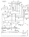
- the acquisition and recording module 10 shown diagrammatically in FIG. 1 is contained in a boardable housing provided with a connector 12 for data input and with a connector 14 for connection to a test and read unit 16.
- the message then consists of successive sequences each having an initial synchronization word Sy consisting of two bytes Sy1 and Sy2 of determined value, for example FB and 30 (in hexadecimal). The eight bytes each representing an analog signal sample ANA1, ...
- ANA8 are transmitted in two groups, separated by a NUM byte consisting of eight bits representative of binary signals to be acquired and an incrementation index ID.
- the latter gives the serial number, and therefore the date, of a sequence in writing when an event is memorized in real time and the memory address where the sequence is stored.
- the module 10 includes supply circuits 18 allowing, from an external source, to generate the different voltages necessary for operation.
- analog inputs are connected, via a multiplexer 20, to an analog / digital converter or ADC 22 providing, to an acquisition block 24, each sample in turn in the form of a byte (or multiple bytes).
- ADC 22 provides, to an acquisition block 24, each sample in turn in the form of a byte (or multiple bytes).
- Each of the binary data inputs drives the acquisition unit via an octoelectronic coupler 26 of galvanic isolation.
- the data acquisition rate is fixed by an internal clock 30, at 144 KHz for example, and by a time base 32 providing, by division of the clock frequency, a word clock DDD and a clock of sequence S
- the clock S fixes the operating rate of the analog-digital converter 22.
- the division ratios can be fixed by wiring the connector 14 or by acquiring external commands, before operation.
- the module may include an external command acquisition circuit 34 having an input connected to the connector 14 to authorize either a selection wiring before operation or an instruction acquisition, indicated by the arrow 36.
- the acquisition circuit 34 is also provided to receive from the unit 16, when it is connected, a signal passing the module 10 from the recording mode to the reading mode or to the memory erasing mode.
- the operation of the module is controlled by a microcontroller 38 associated with a program read-only memory and with an erasable non-volatile recording memory 42, generally constituted by an electrically erasable read-only memory or EEROM.
- the memory 42 can in particular have a write cycle of 150 ⁇ s and have a capacity of 64 K bytes by analog or digital input channel, making it possible to record for 40 seconds at the rate of 1500 sequences per second.
- the rhythm can be modified and for example control 12 sequences per second, bringing the recording time to 86 minutes.
- the acquisition unit 24 and the microcontroller 38 are connected by a bus 44 to which is also connected a parallel / serial interface 46 supplying an output 48 on the connector 14, which avoids the need for bus contacts on the connector 14
- the interface 46 serializes the bits of each of the bytes of the sequences read successively in EEROM memory, when the module is in read mode, and then supplies the successive sequences in PCM coding, for example with the format shown in FIG. 2.
- This format allows various variants and, in particular, allows an over-switching by a factor 2 or a factor 4 for one or more analog signals, which makes it possible to increase the sampling rate for these input signals, at the cost of a reduction in the number of analog signals acquired.
- the memory 42 advantageously includes a location 52 for storing a control word.
- the memory is organized so that a predetermined word is written there by the microcontroller 38 from the start of the recording and that this word is erased last if the memory 42 controlled from the unit is erased. 16.
- the microcontroller is programmed so that upon receipt of a write command, it first tests the content of location 52. If a word is written there, it prohibits any writing. Thus, for example in the event of a power cut followed by a restoration, no additional recording erasing the initial recording can be made in the memory 42 due to the re-initialization of the microcontroller 38.
- the memory 42 is advantageously provided so that writing is possible there only if it is preceded by the sending of a code word.
- the microcontroller 38 is also programmed so as to lock the memory 42 by channel software as soon as the total capacity of memory 42 is reached. This avoids disturbances, due for example to a shock at the end of the test.
- Figure 3 shows a timing diagram of the signals being recorded.
- the first and second lines show respectively the signal DDD at the rate of bytes, and the signal S at the rate of transmission of the sequences.
- a word counter 54 (FIG. 1) makes it possible to store the sequence number of the successive bytes and to provide corresponding information on a pin 56 of the connector 14.
- FIG. 3 The lower part of FIG. 3 is a large-scale timing diagram showing the staggering of the signals over the course of a byte.
- An RDA command for selecting status words is sent at the start of the byte and a TP command for selecting interface 46 at the end of the byte.
- the detection of the RDA status word causes the analog-digital converter to operate, which supplies the result to be memorized in a time which must be short enough to authorize the recording.
- the maximum duration can be 15 ⁇ s for a bit duration of 7 ⁇ s.
- the test unit 16 is provided with a connector 58 intended to mate with the connector 14 and with display means 60 (row of light-emitting diodes for example), making it possible to display each of the bytes of the sequences. It also includes control and programming means, constituted for example by selectors and push buttons.
- the unit 16 will generally include a power supply which can replace the power supply 18. It notably makes it possible to verify that the memory 42 is completely erased.
- the unit can be provided to erase the memory 42, for a new recording.
- the module can be provided so that, at the same time as it memorizes the input channels, supplying them on its output for direct transmission, simultaneously allowing telemetry and recording. .
Landscapes
- Physics & Mathematics (AREA)
- General Physics & Mathematics (AREA)
- Read Only Memory (AREA)
- Recording Measured Values (AREA)
Applications Claiming Priority (2)
| Application Number | Priority Date | Filing Date | Title |
|---|---|---|---|
| FR9016123 | 1990-12-21 | ||
| FR909016123A FR2670918B1 (fr) | 1990-12-21 | 1990-12-21 | Dispositif d'enregistrement et de restitution de donnees. |
Publications (1)
| Publication Number | Publication Date |
|---|---|
| EP0493193A1 true EP0493193A1 (de) | 1992-07-01 |
Family
ID=9403552
Family Applications (1)
| Application Number | Title | Priority Date | Filing Date |
|---|---|---|---|
| EP91403426A Withdrawn EP0493193A1 (de) | 1990-12-21 | 1991-12-17 | Vorrichtung zur Datenspeicherung und -wiedergewinnung |
Country Status (2)
| Country | Link |
|---|---|
| EP (1) | EP0493193A1 (de) |
| FR (1) | FR2670918B1 (de) |
Citations (1)
| Publication number | Priority date | Publication date | Assignee | Title |
|---|---|---|---|---|
| US4817049A (en) * | 1985-04-24 | 1989-03-28 | Datapaq, Ltd. | Data logging device with separated data memory unit having internal power source and transducer interface unit for connection to external transducers |
-
1990
- 1990-12-21 FR FR909016123A patent/FR2670918B1/fr not_active Expired - Fee Related
-
1991
- 1991-12-17 EP EP91403426A patent/EP0493193A1/de not_active Withdrawn
Patent Citations (1)
| Publication number | Priority date | Publication date | Assignee | Title |
|---|---|---|---|---|
| US4817049A (en) * | 1985-04-24 | 1989-03-28 | Datapaq, Ltd. | Data logging device with separated data memory unit having internal power source and transducer interface unit for connection to external transducers |
Non-Patent Citations (1)
| Title |
|---|
| INSTITUTION OF ELECTRICAL ENGINEERS INTERNATIONAL CONFERENCE ON MAGNETIC RECORDING 6 July 1964, LONDON GB pages 57 - 59; J.P. LEBEL ET AL.: 'Earth science data acquisition in digital form using audio tape recorders' * |
Also Published As
| Publication number | Publication date |
|---|---|
| FR2670918B1 (fr) | 1994-09-16 |
| FR2670918A1 (fr) | 1992-06-26 |
Similar Documents
| Publication | Publication Date | Title |
|---|---|---|
| EP0044039B1 (de) | Individualisierter, tragbarer Gegenstand der Kreditkartenart | |
| EP0156724B1 (de) | Aufzeichnungsverfahren für einen Plattenspeicher und Plattenspeichersystem | |
| EP0467754B1 (de) | Automatische Ladevorrichtung für ein Geschütz | |
| EP0263019A1 (de) | Flugaufnahmevorrichtung mit elektronischem statischem Speicher | |
| EP0168077A1 (de) | Interface-Schaltung des Sklaven-Typs funktionierend mit einem seriellen Bus | |
| EP1510925A2 (de) | Cache-Speicher mit asynchronem Auslesen und Datenspeicherzugriffssteuerungsvorrichtung mit einem solchen Cache-Speicher | |
| FR2460510A1 (fr) | Appareil de transfert d'informations | |
| FR2678755A1 (fr) | Telecommande a securite optimisee. | |
| FR2542113A1 (fr) | Generateur de graphiques a ordinateur | |
| FR2550677A1 (fr) | Systeme de traduction video pour la traduction d'un signal d'information code binaire en un signal video et inversement | |
| EP0161177A1 (de) | Verfahren und Einrichtung zur Wiedergewinnung des Rahmenverriegelungswortes mit verteilten Bits in einem digitalen Signal | |
| EP0493193A1 (de) | Vorrichtung zur Datenspeicherung und -wiedergewinnung | |
| EP0464768B1 (de) | Schnittstellenmodul für Datenübertragung | |
| FR2476952A1 (fr) | Generateur de signaux de base et de signaux de test de television et systeme comportant un tel dispositif | |
| EP2130097B1 (de) | Verfahren zum zugreifen einen nichtflüchtigen speicher für eine uhr | |
| FR2461294A1 (fr) | Dispositif de modification de programme de sequence | |
| EP0112429A1 (de) | System zur Übertragung von Daten durch sich wiederholende Folgen | |
| FR2648972A1 (fr) | Dispositif de synchronisation pour un decodeur de donnees codees par un code a longueur variable | |
| EP0650267A1 (de) | Übertragungssystem | |
| EP0298793B1 (de) | Schaltung zur Speicherung von Verfügbarkeitszuständen von logischen Betriebsmitteln, wie Speicherzellen und zur Aufstellung von Adressen von freien Betriebsmitteln | |
| FR2646975A1 (fr) | Generateur de donnees numeriques | |
| FR2610033A1 (fr) | Clef et serrure electroniques | |
| EP0635786A1 (de) | Einrichtung zur Speicherung von Daten | |
| EP0449190B1 (de) | Programmschalteinrichtung zur Erzeugung von binären Ausgangssignalen als Reaktion auf ein Taktsignal | |
| FR2607648A1 (fr) | Procede et dispositif de transmission rapide de donnees entre un emetteur et un recepteur par liaison serie standard |
Legal Events
| Date | Code | Title | Description |
|---|---|---|---|
| PUAI | Public reference made under article 153(3) epc to a published international application that has entered the european phase |
Free format text: ORIGINAL CODE: 0009012 |
|
| AK | Designated contracting states |
Kind code of ref document: A1 Designated state(s): BE DE GB IT NL |
|
| 17P | Request for examination filed |
Effective date: 19921007 |
|
| 17Q | First examination report despatched |
Effective date: 19961002 |
|
| STAA | Information on the status of an ep patent application or granted ep patent |
Free format text: STATUS: THE APPLICATION IS DEEMED TO BE WITHDRAWN |
|
| 18D | Application deemed to be withdrawn |
Effective date: 19970415 |