EP0493835A2 - Arithmetische Operationseinheit mit Bit-Invertierungsfunktion - Google Patents
Arithmetische Operationseinheit mit Bit-Invertierungsfunktion Download PDFInfo
- Publication number
- EP0493835A2 EP0493835A2 EP91122381A EP91122381A EP0493835A2 EP 0493835 A2 EP0493835 A2 EP 0493835A2 EP 91122381 A EP91122381 A EP 91122381A EP 91122381 A EP91122381 A EP 91122381A EP 0493835 A2 EP0493835 A2 EP 0493835A2
- Authority
- EP
- European Patent Office
- Prior art keywords
- carry
- arithmetic operation
- gate
- signal
- operation unit
- Prior art date
- Legal status (The legal status is an assumption and is not a legal conclusion. Google has not performed a legal analysis and makes no representation as to the accuracy of the status listed.)
- Granted
Links
Images


Classifications
-
- G—PHYSICS
- G06—COMPUTING OR CALCULATING; COUNTING
- G06F—ELECTRIC DIGITAL DATA PROCESSING
- G06F7/00—Methods or arrangements for processing data by operating upon the order or content of the data handled
- G06F7/38—Methods or arrangements for performing computations using exclusively denominational number representation, e.g. using binary, ternary, decimal representation
- G06F7/48—Methods or arrangements for performing computations using exclusively denominational number representation, e.g. using binary, ternary, decimal representation using non-contact-making devices, e.g. tube, solid state device; using unspecified devices
- G06F7/50—Adding; Subtracting
- G06F7/501—Half or full adders, i.e. basic adder cells for one denomination
- G06F7/503—Half or full adders, i.e. basic adder cells for one denomination using carry switching, i.e. the incoming carry being connected directly, or only via an inverter, to the carry output under control of a carry propagate signal
-
- G—PHYSICS
- G06—COMPUTING OR CALCULATING; COUNTING
- G06F—ELECTRIC DIGITAL DATA PROCESSING
- G06F7/00—Methods or arrangements for processing data by operating upon the order or content of the data handled
- G06F7/38—Methods or arrangements for performing computations using exclusively denominational number representation, e.g. using binary, ternary, decimal representation
- G06F7/48—Methods or arrangements for performing computations using exclusively denominational number representation, e.g. using binary, ternary, decimal representation using non-contact-making devices, e.g. tube, solid state device; using unspecified devices
- G06F7/57—Arithmetic logic units [ALU], i.e. arrangements or devices for performing two or more of the operations covered by groups G06F7/483 – G06F7/556 or for performing logical operations
- G06F7/575—Basic arithmetic logic units, i.e. devices selectable to perform either addition, subtraction or one of several logical operations, using, at least partially, the same circuitry
-
- G—PHYSICS
- G06—COMPUTING OR CALCULATING; COUNTING
- G06F—ELECTRIC DIGITAL DATA PROCESSING
- G06F2207/00—Indexing scheme relating to methods or arrangements for processing data by operating upon the order or content of the data handled
- G06F2207/38—Indexing scheme relating to groups G06F7/38 - G06F7/575
- G06F2207/3804—Details
- G06F2207/3808—Details concerning the type of numbers or the way they are handled
- G06F2207/3852—Calculation with most significant digit first
Definitions
- the present invention relates to a digital arithmetic operation unit, and more specifically to an arithmetic operation unit having a bit inversion function capable of executing a given arithmetic operation in a bit-inverted condition.
- a result of operation of one of the two independent arithmetic operation units is selected on the basis of the kind of a required arithmetic operation.
- bit-inversion arithmetic operation unit which has overcome the above mentioned defect of the conventional one and which can be constituted of a reduced amount of hardware.
- a bit-inversion arithmetic operation unit comprising a first carry signal line for propagating a carry signal from a more significant bit position side to a less significant bit position side; a second carry signal line for propagating a carry signal from a less significant bit position side to a more significant bit position side; a common logic circuit for performing at least a portion of a carry control including a carry propagation of the first and second carry signals and a carry generation; and a switching and logic circuit responding to a required arithmetic operation mode for controlling the common logic circuit and for performing the remaining portion of the carry control including the carry propagation of the first and second carry signals and the carry generation.
- the bit-inversion arithmetic operation unit in accordance with the present invention can be constituted of a reduced amount of hardware.
- FIG. 1 there is shown a logic diagram of a one-bit arithmetic operation unit of a first embodiment of the bit-inversion arithmetic operation unit in accordance with the present invention.
- a pair of input terminals 101 ands 102 are connected to each of a NOR gate 109 and a NAND gate 110.
- a first carry input terminal 103 is connected through a transfer gate 115 to a first carry output terminal 106
- a second carry input terminal 104 is connected through a transfer gate 116 to a second carry output terminal 107.
- the first carry output terminal 106 is pulled up through a P-channel MOS transistor 111 to a high voltage V DD and also pulled down through an N-channel MOS transistor 113 to a ground GND
- the second carry output terminal 107 is pulled up through a P-channel MOS transistor 112 to the high voltage V DD and also pulled down through an N-channel MOS transistor 114 to the ground GND.
- Each of the two pull-up transistors 111 and 112 has a gate connected to an output of the NAND gate 110
- each of the two pull-down transistors 113 and 114 has a gate connected to an output of the NOR gate 109.
- the pair of input terminals 101 and 102 are connected to a carry propagation control circuit 117, which generates a first carry propagation control signal 121 and a second carry propagation control signal 122.
- the first carry propagation control signal 121 is connected to a gate of an N-channel MOS transistor of each of the transfer gates 115 and 116 and also to one input of each of a pair of exclusive-OR gates 118 and 119.
- the second carry propagation control signal 122 is connected to a gate of a P-channel MOS transistor of each of the transfer gates 115 and 116.
- the other input of the exclusive-OR gate 119 is connected to the first carry input terminal 103, and the other input of the exclusive-OR gate 118 is connected to the second carry input terminal 104.
- Outputs of the exclusive-OR gates 118 and 119 are connected to a selector 120, which has a selection control input connected to a control terminal 105 and an output connected to an output terminal 108.
- the carry propagation control circuit 117 If a pair of input signals "a” and “b” are supplied to the input terminals 101 and 102, respectively, the carry propagation control circuit 117 generates the carry propagation control signals 121 and 122, and at the same time, a logical sum and a logical product of the input signals "a” and “b” are generated by the logic gates 109 and 110.
- the transfer gate 115 is opened by the first and second carry propagation control signals 121 and 122 so as to cause a first carry input signal C in1 to be propagated to the terminal 106, so that the logic level of the first carry output signal C o1 is determined by the first carry input signal C in1 inputted to the terminal 103.
- the exclusive-OR gate 119 generates an exclusive-OR of the first carry input signal C in1 and the first carry propagation control signal 121, so that the generated exclusive-OR signal is supplied to the selector 120.
- the transfer gate 116 is opened by the first and second carry propagation control signals 121 and 122 so as to cause a second carry input signal C in2 to be propagated to the terminal 107, so that the logic level of the second catty output signal C o2 is determined by the second carry input signal C in2 inputted to the terminal 104.
- the exclusive-OR gate 118 generates an exclusive-OR of the second carry input signal C in2 and the first carry propagation control signal 121, so that the generated exclusive-OR signal is supplied to the selector 120.
- either the sum signal of the bit-inversion arithmetic operation or the sum signal of the normal arithmetic operation is selected by the selector 120 in accordance with the selection control signal "cont", and namely, is supplied as an output of the one-bit arithmetic operation unit.
- FIG 2 there is shown one example of a four-bit bit-inversion arithmetic operation unit composed of one-bit arithmetic operation units shown in Figure 1.
- Two items of four-bit data are composed of bits “a0” to “a3” and bits “b0” to “b3”, respectively.
- the input bits “a0” to “a3” are supplied to four input terminals 301 to 304, respectively, and the input bits “b0” to “b3” are supplied to four input terminals 305 to 308, respectively, so that input bit pairs "a0” and “b0”, “a1” and “b1”, “a2” and “b2”, and "a3” and “b3” are supplied to four one-bit arithmetic operation units 309, 310, 311 and 312, respectively.
- a first carry input terminal 313 and a second carry output terminal 316 are connected to a first carry input terminal C in1 and the second carry output terminal C o2 of the one-bit arithmetic operation unit 312, and a second carry input terminal 314 and a first carry output terminal 315 are connected to a second carry input terminal C in2 and the first carry output terminal C o1 of the one-bit arithmetic operation unit 309.
- each pair of adjacent one-bit arithmetic operation units are connected in such a manner that a first carry output terminal C o1 and a second carry input terminal C in2 of a more significant bit side one-bit arithmetic operation unit are connected to a first carry input terminal C in1 and a second carry output terminal C o2 of a less significant bit side one-bit arithmetic operation unit, respectively.
- the four one-bit arithmetic operation units 309, 310, 311 and 312 are connected to receive a common control signal "cont" supplied to a control terminal 318, so that a selected one of a normal arithmetic operation result and a bit-inversion arithmetic operation result is outputted in the form of four output bits "r0" to "r3" to four output terminals 319, 320, 321, and 322.
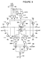
- FIG 3 there is shown a logic diagram of a one-bit arithmetic operation unit of a second embodiment of the bit-inversion arithmetic operation unit in accordance with the present invention.
- elements similar to those shown in Figure 1 are given the same Reference Numerals, and therefore, explanation thereof will be omitted.
- the carry propagation control circuit 117 is replaced with a NOR gate 218 connected to the pair of input data bit terminals 101 and 102, a "3 and 2" NOR gate 217 connected to an output of the NOR gate 218 and the pair of input data bit terminals 101 and 102 and outputting a carry propagation control signal 228 corresponding to the first carry propagation control signal 121, and an inverter 219 receiving an output of the gate 217 and outputting a carry propagation control signal 229 corresponding to the second carry propagation control signal 122.
- the "3 and 2" NOR gate 217 can be expressed by an AND gate 217A receiving the pair of input data bit terminals 101 and 102, and a NOR gate 217B receiving an output of the NOR gate 218 and an output of the AND gate 217B.
- the exclusive-OR gate 119 which receives the first carry input signal C in1 and the first carry propagation control signal 121 and generates an exclusive-OR thereof, is constituted of a NOR gate 223 receiving the first carry input signal C in1 and the first carry propagation control signal 228, and a "3 and 2" NOR gate 222 receiving an output of the NOR gate 223 and tile first carry input signal C in1 and the first carry propagation control signal 228.
- the "3 and 2" NOR gate 222 can be expressed by an AND gate 222A and a NOR gate 222B connected as shown.
- the exclusive-OR gate 118 which receives the second carry input signal C in2 and the first carry propagation control signal 121 and generates an exclusive-OR thereof, is constituted of a NOR gate 221 receiving the second carry input signal C in2 and the first carry propagation control signal 228, and a "3 and 2" NOR gate 220 receiving an output of the NOR gate 221 and the second carry input signal C in2 and the first carry propagation control signal 228.
- the "3 and 2" NOR gate 220 can be expressed by an AND gate 220A and a NOR gate 220B connected as shown.
- the selector 120 is composed of a tristate inverter 225 having an input connected to an output of the "3 and 2" NOR gate 220, and another tristate inverter 226 having an input connected to an output of the "3 and 2" NOR gate 222, and an inverter having an input connected in common to an output of the tristate inverter 225 and an output of the tristate inverter 226 and having an output connected to the output terminal 108.
- the selection control terminal 105 is connected directly to a non-inverting control input of the tristate inverter 225 and an inverting control input of the tristate inverter 226.
- the selection control terminal 105 is also connected through an inverter 224 to an inverting control input of the tristate inverter 225 and a non-inverting control input of the tristate inverter 226.
- the second embodiment shown in Figure 3 operates similarly to the first embodiment shown in Figure 1, and therefore, the four-bit bit-inversion arithmetic operation unit can be formed using four one-bit arithmetic operation units each of which is the same as that shown in Figure 3.
Landscapes
- Physics & Mathematics (AREA)
- General Physics & Mathematics (AREA)
- Engineering & Computer Science (AREA)
- Computational Mathematics (AREA)
- Mathematical Analysis (AREA)
- Pure & Applied Mathematics (AREA)
- Theoretical Computer Science (AREA)
- Mathematical Optimization (AREA)
- Computing Systems (AREA)
- General Engineering & Computer Science (AREA)
- Logic Circuits (AREA)
Applications Claiming Priority (2)
| Application Number | Priority Date | Filing Date | Title |
|---|---|---|---|
| JP2417201A JPH04230521A (ja) | 1990-12-29 | 1990-12-29 | ビット反転演算器 |
| JP417201/90 | 1990-12-29 |
Publications (3)
| Publication Number | Publication Date |
|---|---|
| EP0493835A2 true EP0493835A2 (de) | 1992-07-08 |
| EP0493835A3 EP0493835A3 (en) | 1993-05-05 |
| EP0493835B1 EP0493835B1 (de) | 1998-12-16 |
Family
ID=18525327
Family Applications (1)
| Application Number | Title | Priority Date | Filing Date |
|---|---|---|---|
| EP91122381A Expired - Lifetime EP0493835B1 (de) | 1990-12-29 | 1991-12-30 | Arithmetische Operationseinheit mit Bit-Invertierungsfunktion |
Country Status (4)
| Country | Link |
|---|---|
| US (1) | US5224065A (de) |
| EP (1) | EP0493835B1 (de) |
| JP (1) | JPH04230521A (de) |
| DE (1) | DE69130640T2 (de) |
Families Citing this family (21)
| Publication number | Priority date | Publication date | Assignee | Title |
|---|---|---|---|---|
| US5267187A (en) * | 1990-05-10 | 1993-11-30 | Xilinx Inc | Logic structure and circuit for fast carry |
| KR960004572B1 (ko) * | 1994-01-28 | 1996-04-09 | 금성일렉트론주식회사 | 산술연산 논리회로 |
| US5442577A (en) * | 1994-03-08 | 1995-08-15 | Exponential Technology, Inc. | Sign-extension of immediate constants in an alu |
| US7284222B1 (en) * | 2004-06-30 | 2007-10-16 | Tabula, Inc. | Method and apparatus for identifying connections between configurable nodes in a configurable integrated circuit |
| US7312630B2 (en) | 2004-06-30 | 2007-12-25 | Tabula, Inc. | Configurable integrated circuit with built-in turns |
| US7282950B1 (en) * | 2004-11-08 | 2007-10-16 | Tabula, Inc. | Configurable IC's with logic resources with offset connections |
| US7743085B2 (en) * | 2004-11-08 | 2010-06-22 | Tabula, Inc. | Configurable IC with large carry chains |
| US7917559B2 (en) * | 2004-11-08 | 2011-03-29 | Tabula, Inc. | Configurable IC's with configurable logic circuits that perform adder and/or subtractor operations |
| US7298169B2 (en) * | 2005-03-15 | 2007-11-20 | Tabula, Inc | Hybrid logic/interconnect circuit in a configurable IC |
| US20070244959A1 (en) * | 2005-03-15 | 2007-10-18 | Steven Teig | Configurable IC's with dual carry chains |
| US7530033B2 (en) | 2005-03-15 | 2009-05-05 | Tabula, Inc. | Method and apparatus for decomposing functions in a configurable IC |
| US7825684B2 (en) * | 2005-03-15 | 2010-11-02 | Tabula, Inc. | Variable width management for a memory of a configurable IC |
| US7310003B2 (en) * | 2005-03-15 | 2007-12-18 | Tabula, Inc. | Configurable IC with interconnect circuits that have select lines driven by user signals |
| US8463836B1 (en) | 2005-11-07 | 2013-06-11 | Tabula, Inc. | Performing mathematical and logical operations in multiple sub-cycles |
| US7818361B1 (en) | 2005-11-07 | 2010-10-19 | Tabula, Inc. | Method and apparatus for performing two's complement multiplication |
| US7765249B1 (en) | 2005-11-07 | 2010-07-27 | Tabula, Inc. | Use of hybrid interconnect/logic circuits for multiplication |
| US7797497B1 (en) * | 2006-03-08 | 2010-09-14 | Tabula, Inc. | System and method for providing more logical memory ports than physical memory ports |
| US7694083B1 (en) * | 2006-03-08 | 2010-04-06 | Tabula, Inc. | System and method for providing a virtual memory architecture narrower and deeper than a physical memory architecture |
| US7930666B1 (en) | 2006-12-12 | 2011-04-19 | Tabula, Inc. | System and method of providing a memory hierarchy |
| US10756753B2 (en) * | 2018-10-25 | 2020-08-25 | Arm Limited | Data compressor logic circuit |
| CN117453178B (zh) * | 2023-03-20 | 2024-08-02 | 中科南京智能技术研究院 | 一种计算x'|(x-1)的专用加速器及加速计算装置 |
Family Cites Families (5)
| Publication number | Priority date | Publication date | Assignee | Title |
|---|---|---|---|---|
| JP2610417B2 (ja) * | 1985-12-23 | 1997-05-14 | 日本テキサス・インスツルメンツ株式会社 | アドレス信号生成方法及びその回路 |
| IT1210751B (it) * | 1987-05-20 | 1989-09-20 | Cselt Centro Studi Lab Telecom | Sommatore veloce in tecnologia c mos |
| JPH01180633A (ja) * | 1988-01-12 | 1989-07-18 | Mitsubishi Electric Corp | 加算器 |
| JPH0679269B2 (ja) * | 1988-05-20 | 1994-10-05 | 三菱電機株式会社 | 加算器 |
| US4974188A (en) * | 1988-12-09 | 1990-11-27 | The Johns Hopkins University | Address sequence generation by means of reverse carry addition |
-
1990
- 1990-12-29 JP JP2417201A patent/JPH04230521A/ja active Pending
-
1991
- 1991-12-30 US US07/814,719 patent/US5224065A/en not_active Expired - Lifetime
- 1991-12-30 EP EP91122381A patent/EP0493835B1/de not_active Expired - Lifetime
- 1991-12-30 DE DE69130640T patent/DE69130640T2/de not_active Expired - Fee Related
Also Published As
| Publication number | Publication date |
|---|---|
| US5224065A (en) | 1993-06-29 |
| DE69130640D1 (de) | 1999-01-28 |
| EP0493835A3 (en) | 1993-05-05 |
| JPH04230521A (ja) | 1992-08-19 |
| EP0493835B1 (de) | 1998-12-16 |
| DE69130640T2 (de) | 1999-07-22 |
Similar Documents
| Publication | Publication Date | Title |
|---|---|---|
| US5224065A (en) | Arithmetic operation unit having bit inversion function | |
| JP2540934B2 (ja) | 論理回路装置 | |
| US4709226A (en) | Circuitry for complementing binary numbers | |
| US5487025A (en) | Carry chain adder using regenerative push-pull differential logic | |
| US4701877A (en) | Highspeed parallel adder with clocked switching circuits | |
| US5548231A (en) | Serial differential pass gate logic design | |
| US5546035A (en) | Latch circuit having a logical operation function | |
| EP0751457B1 (de) | Basiszelle zum Vergleichen eines ersten und eines zweiten digitalen Signals und entsprechender digitaler Komparator | |
| US6066978A (en) | Partial product generating circuit | |
| US4704701A (en) | Conditional carry adder for a multibit digital computer | |
| US5148057A (en) | Circuit apparatus for detecting preceding value one | |
| US5140546A (en) | Adder circuit apparatus | |
| AU720687B2 (en) | Logic circuits | |
| US6731138B2 (en) | Circuits and methods for selectively latching the output of an adder | |
| US5596520A (en) | CMOS full adder circuit with pair of carry signal lines | |
| JP3355513B2 (ja) | 論理回路 | |
| US5726928A (en) | Arithmetic logic unit circuit with reduced propagation delays | |
| US6219686B1 (en) | Method and apparatus for an N-NARY sum/HPG adder/subtractor gate | |
| KR100278992B1 (ko) | 전가산기 | |
| KR100230399B1 (ko) | 입력값 특성을 이용한 덧셈기 | |
| JP2599689B2 (ja) | キャリ伝達装置 | |
| US6567836B1 (en) | Multi-level carry-skip adder | |
| JPH0616263B2 (ja) | バレルシフタ | |
| JPH0462499B2 (de) | ||
| JPH0879056A (ja) | 論理回路 |
Legal Events
| Date | Code | Title | Description |
|---|---|---|---|
| PUAI | Public reference made under article 153(3) epc to a published international application that has entered the european phase |
Free format text: ORIGINAL CODE: 0009012 |
|
| AK | Designated contracting states |
Kind code of ref document: A2 Designated state(s): DE FR GB |
|
| 17P | Request for examination filed |
Effective date: 19920629 |
|
| PUAL | Search report despatched |
Free format text: ORIGINAL CODE: 0009013 |
|
| AK | Designated contracting states |
Kind code of ref document: A3 Designated state(s): DE FR GB |
|
| 17Q | First examination report despatched |
Effective date: 19970618 |
|
| GRAG | Despatch of communication of intention to grant |
Free format text: ORIGINAL CODE: EPIDOS AGRA |
|
| GRAG | Despatch of communication of intention to grant |
Free format text: ORIGINAL CODE: EPIDOS AGRA |
|
| GRAH | Despatch of communication of intention to grant a patent |
Free format text: ORIGINAL CODE: EPIDOS IGRA |
|
| GRAH | Despatch of communication of intention to grant a patent |
Free format text: ORIGINAL CODE: EPIDOS IGRA |
|
| GRAA | (expected) grant |
Free format text: ORIGINAL CODE: 0009210 |
|
| AK | Designated contracting states |
Kind code of ref document: B1 Designated state(s): DE FR GB |
|
| REF | Corresponds to: |
Ref document number: 69130640 Country of ref document: DE Date of ref document: 19990128 |
|
| ET | Fr: translation filed | ||
| PLBE | No opposition filed within time limit |
Free format text: ORIGINAL CODE: 0009261 |
|
| STAA | Information on the status of an ep patent application or granted ep patent |
Free format text: STATUS: NO OPPOSITION FILED WITHIN TIME LIMIT |
|
| 26N | No opposition filed | ||
| REG | Reference to a national code |
Ref country code: GB Ref legal event code: IF02 |
|
| REG | Reference to a national code |
Ref country code: GB Ref legal event code: 732E |
|
| REG | Reference to a national code |
Ref country code: FR Ref legal event code: TP |
|
| PGFP | Annual fee paid to national office [announced via postgrant information from national office to epo] |
Ref country code: FR Payment date: 20081212 Year of fee payment: 18 |
|
| PGFP | Annual fee paid to national office [announced via postgrant information from national office to epo] |
Ref country code: DE Payment date: 20081229 Year of fee payment: 18 |
|
| PGFP | Annual fee paid to national office [announced via postgrant information from national office to epo] |
Ref country code: GB Payment date: 20081224 Year of fee payment: 18 |
|
| GBPC | Gb: european patent ceased through non-payment of renewal fee |
Effective date: 20091230 |
|
| REG | Reference to a national code |
Ref country code: FR Ref legal event code: ST Effective date: 20100831 |
|
| PG25 | Lapsed in a contracting state [announced via postgrant information from national office to epo] |
Ref country code: FR Free format text: LAPSE BECAUSE OF NON-PAYMENT OF DUE FEES Effective date: 20091231 |
|
| PG25 | Lapsed in a contracting state [announced via postgrant information from national office to epo] |
Ref country code: DE Free format text: LAPSE BECAUSE OF NON-PAYMENT OF DUE FEES Effective date: 20100701 |
|
| PG25 | Lapsed in a contracting state [announced via postgrant information from national office to epo] |
Ref country code: GB Free format text: LAPSE BECAUSE OF NON-PAYMENT OF DUE FEES Effective date: 20091230 |