EP0495632A2 - Afficheur à cristal liquide - Google Patents
Afficheur à cristal liquide Download PDFInfo
- Publication number
- EP0495632A2 EP0495632A2 EP92300315A EP92300315A EP0495632A2 EP 0495632 A2 EP0495632 A2 EP 0495632A2 EP 92300315 A EP92300315 A EP 92300315A EP 92300315 A EP92300315 A EP 92300315A EP 0495632 A2 EP0495632 A2 EP 0495632A2
- Authority
- EP
- European Patent Office
- Prior art keywords
- electrodes
- liquid crystal
- electrode
- conductive film
- substrates
- Prior art date
- Legal status (The legal status is an assumption and is not a legal conclusion. Google has not performed a legal analysis and makes no representation as to the accuracy of the status listed.)
- Granted
Links
Images


Classifications
-
- G—PHYSICS
- G02—OPTICS
- G02F—OPTICAL DEVICES OR ARRANGEMENTS FOR THE CONTROL OF LIGHT BY MODIFICATION OF THE OPTICAL PROPERTIES OF THE MEDIA OF THE ELEMENTS INVOLVED THEREIN; NON-LINEAR OPTICS; FREQUENCY-CHANGING OF LIGHT; OPTICAL LOGIC ELEMENTS; OPTICAL ANALOGUE/DIGITAL CONVERTERS
- G02F1/00—Devices or arrangements for the control of the intensity, colour, phase, polarisation or direction of light arriving from an independent light source, e.g. switching, gating or modulating; Non-linear optics
- G02F1/01—Devices or arrangements for the control of the intensity, colour, phase, polarisation or direction of light arriving from an independent light source, e.g. switching, gating or modulating; Non-linear optics for the control of the intensity, phase, polarisation or colour
- G02F1/13—Devices or arrangements for the control of the intensity, colour, phase, polarisation or direction of light arriving from an independent light source, e.g. switching, gating or modulating; Non-linear optics for the control of the intensity, phase, polarisation or colour based on liquid crystals, e.g. single liquid crystal display cells
- G02F1/133—Constructional arrangements; Operation of liquid crystal cells; Circuit arrangements
- G02F1/1333—Constructional arrangements; Manufacturing methods
- G02F1/1343—Electrodes
- G02F1/134309—Electrodes characterised by their geometrical arrangement
- G02F1/134336—Matrix
Definitions
- the present invention relates to a liquid crystal display using a ferroelectric liquid crystal, for example.
- display means have played an important part as means for transmitting information.
- a typical example of conventional display means is a CRT (cathode ray tube).
- a liquid crystal display has widely been utilized for the merit that its structure can be miniaturized and power consumption can be reduced. Furthermore, it is greatly desired that a liquid crystal display device having a larger display area and a larger capacity should be realized.
- a liquid crystal display using a ferroelectric liquid crystal has the most potential to realize such desire.
- a chiral smectic liquid crystal is normally used for the ferroelectric liquid crystal.
- a ferroelectric chiral smectic phase takes a helical structure in molecular configuration. When being put into a thin cell, the helical structure is affected and comes loose by an interface. Consequently, with reference to Figs. 10 (a), (b) and (c), liquid crystal molecules 18 form two domains, that is, a domain inclined from a smectic layer normal 17 by an angle of + ⁇ 19 and a domain inclined in the symmetrically opposite direction by an angle of - ⁇ 20 as shown in Fig. 10 (a).
- a liquid crystal display can essentially be structured by addition of a polarizing plate.
- a pair of translucent or transparent substrates 21 and 22 each has stripe-shaped transparent electrodes 23 and 24 which are provided on opposite faces of the substrates 21 and 22 respectively. And in setting up these translucent substrates 21 and 22 opposite to each other, the transparent electrodes 23 and 24 are provided to form a matrix electrode structure. Orientation films 27 and 28 are layered on the transparent electrodes 23 and 24 respectively with insulating films 25 and 26 inbetween. A ferroelectric liquid crystal 29 is filled between the translucent substrates 21 and 22. Polarizing plates 30 and 31 are provided on the outer surfaces of the translucent substrates 21 and 22. Thus, a ferroelectric liquid crystal display 32 is formed.
- a ferroelectric liquid crystal display Referring to another problem included in a ferroelectric liquid crystal display according to the prior art, it is that the memory state in a picture element is inverted. That is, when an electric field is applied as shown in Fig. 10 (d), a switch is turned on as shown in Fig. 10 (b) and the electric field is then removed, the state shown in Fig. 10 (d) is returned instead of staying at Fig. 10 (b). There has been described that this phenomenon occurs owing to a reverse electric field which is generated by the spontaneous polarization of the ferroelectric liquid crystal [Yoshida et al; Collection of Papers Presented to 13th Liquid Crystal Symposium, 2Z15 (1987)].
- a metal or the like wiring provided on the transparent electrode causes undesirable narrowing of the transparent portion or area of the electrode. Consequently, the active or utilizable aperture of the display is lowered.
- the film thickness of the metal or the like is increased so that a line width is reduced in order to prevent the active aperture from being lowered, there is increased a possibility that electric contact is caused between upper and lower translucent substrates. Consequently, display grade is impaired. This is not an important problem for a twisted nematic (TN) liquid crystal display having a comparatively great cell thickness, but this is serious for a ferroelectric liquid crystal display which needs such a thin cell thickness as 0.5 to 4 ⁇ m, preferably 2 ⁇ m or less.
- TN twisted nematic
- the electrode resistance should be reduced by the low-resistance conductive film such as a metal or the like in order to make the display characteristics uniform.
- the active aperture is lowered in preventing the memory inversion. Consequently, there is increased a possibility that the electric contact is caused between the upper and lower transparent substrates. As a result, the display grade is lowered.
- the present invention provides a liquid crystal display comprising first and second translucent substrates opposed to each other, first and second transparent electrodes formed on opposite faces of the first and second substrates respectively, first and second orientation films formed on the opposite faces of the first and second so as to cover the first and second transparent electrodes, a liquid crystal disposed in a space between the orientation films, the first electrode being divided into a plurality of dot electrodes arranged in row and column directions, and the second electrode being divided into a plurality of stripe electrodes arranged opposite to the dot electrodes of the first electrode in the row direction, a first conductive film for serially connecting the dot electrodes in each column, and a second conductive film provided along the longitudinal edge of the stripe electrode, wherein the first and second substrates are positionally set such that the second conductive film is opposed to concave portions formed between the dot electrodes in the row direction.
- the present invention further provides a liquid crystal display comprising first and second translucent substrates opposed to each other, first and second transparent electrodes formed on opposite faces of the first and second substrates respectively, first and second orientation films formed on the opposite faces of said first and second substrates, so as to cover the first and second transparent electrodes, a liquid crystal filled in a space between the orientation films, the first and second electrodes being divided into a plurality of dot electrodes arranged in row and column directions so as to be opposed to each other, a first conductive film for serially connecting the edges of the dot electrodes of the first electrode at each row, and a second conductive film for serially connecting the edges of the dot electrodes of the second electrode at each column, wherein the first and second substrates are positionally set such that the first conductive film is opposed to concave portions formed between the dot electrodes of the second electrode in the row direction and the second conductive film is opposed to concave portions formed between the dot electrodes of the first electrode in the column direction.
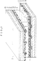
- Fig. 1 is a section view showing the schematic structure of a liquid crystal display according to a first embodiment of the present invention.
- a ferroelectric liquid crystal display 1 comprises a pair of translucent substrates 2 and 3, dot electrodes 5, stripe transparent electrodes 6, low-resistance conductive films 7 and 8, orientation films 11 and 12, a ferroelectric liquid crystal 4, and polarizing plates 13 and 14.
- the translucent substrates 2 and 3 are provided opposite to each other.
- the dot electrodes 5 are transparent electrodes which are formed in a matrix on a surface of the translucent substrate 2 opposite the translucent substrate 3.
- the stripe transparent electrodes 6 are formed in a row direction at equal spaces on a surface of the translucent substrate 3 opposite to the translucent substrate 2.
- the low-resistance conductive films 7 are provided along side edges on the surfaces of the dot electrodes 5 in the column direction and electrically connect the dot electrodes 5 respectively.
- the low-resistance conductive films 8 are provided along and in contact with side edges on the surfaces of the stripe transparent electrodes 6.
- the orientation films 11 and 12 cover the dot electrodes 5 and the stripe transparent electrodes 6 through insulating films 9 and 10, respectively.
- the ferroelectric liquid crystal 4 is disposed between the orientation films 11 and 12.
- the polarizing plates 13 and 14 are provided on an outer surface of the translucent substrates 2 and 3, respectively.
- the translucent substrates 2 and 3 are provided opposite to each other such that the low-resistance conductive films 8 on the stripe transparent electrodes 6 are positioned above trench portions between the dot electrodes 5.
- a typical example of the translucent substrates 2 and 3 is glass.
- the dot electrode 5 and the stripe transparent electrodes are formed of an indium tin oxide (ITO) film.
- ITO indium tin oxide
- the thickness of the ITO film is 2000 ⁇ .
- the low-resistance conductive films 7 and 8 are typically formed by depositing molybdenum with the use of a sputtering method, and have a thickness of 2200 ⁇ and a width of 5 ⁇ m.
- the dot electrode 5 is a square having a side length of 55 ⁇ m. A space between the dot electrodes 5 is 10 ⁇ m
- Fig. 2 is a section view showing the schematic structure of a liquid crystal display according to a second embodiment of the present invention.
- a ferroelectric liquid crystal display 1a comprises translucent substrates 2 and 3 such as glass.
- a ferroelectric liquid crystal 4 is disposed between the orientation films 11 and 12.
- Dot electrodes 5a and 5b are provided as transparent electrodes on opposite faces of the translucent substrates 2 and 3, respectively.
- the dot electrodes 5a and 5b are both arranged in a matrix.
- Low-resistance conductive films 7 and 8 are formed so as to connect the edges of the dot electrodes 5a and 5b for each row and each column. On each low-resistance conductive film 7 and 8 are sequentially provided an insulating film 9 and 10 and an orientation film 11 and 12.
- the translucent substrates 2 and 3 are laminated as shown by an arrow in Fig. 2 such that the concave portions of the low-resistance conductive films 7 and 8 are opposed to each other in the outside direction of the translucent substrates 2 and 3, the low-resistance conductive films 7 are opposed to concave portions formed between the dot electrodes 5b in the row direction and the low-resistance conductive films 8 are opposed to concave portions formed between the dot electrodes 5a in the column direction.
- Polarizing plates 13 and 14 are provided as crossed nicols on the outer surfaces of the translucent substrates 2 and 3.
- ITO and molybdenum are deposited as the dot electrodes 5a and 5b and the low-resistance conductive films 7 and 8 on the translucent substrates 2 and 3 by sputtering respectively, and are then etched so as to have a configuration shown in Fig. 2.
- Figs. 3 (a) to (f) are views showing steps of forming the dot electrodes 5a and 5b and the low-resistance conductive films 7 and 8 on the translucent substrates 2 and 3 in the liquid crystal display 1a according to the second embodiment. Only the case of the translucent substrate 2 is shown in Figs. 3 (a) to (f).
- an ITO film 5c is formed as a dot electrode 5 at a thickness of 2000 ⁇ on a translucent substrate 2 by sputtering.
- a photoresist 16 is applied on the ITO film 5c.
- temporary burning is carried out at a temperature of 90°C.
- Exposure is carried out by a high pressure mercury lamp with the use of a photomask 35 having a shape shown in Fig. 3 (a) so as to perform development. Thereafter, regular burning is carried out at a temperature of 120°C. Consequently, a photoresist is formed as shown in Fig. 3 (b).
- etching is carried out for 4 minutes at a temperature of 35°C by using a solution containing oxalic acid in an amount of 47 %, so that squares shown in Fig. 3 (c) are obtained by patterning.
- a molybdenum film 7a is formed at a thickness of 2200 ⁇ by sputtering.
- the photoresist 16 is applied on the molybdenum film 7a in similar to the case of the ITO film 5c.
- temporary burning is carried out. Exposure is carried out by means of a photomask 36 shown in Fig. 3 (e). Development and regular burning are sequentially carried out.
- etching is carried out for 3 minutes at a temperature of 25°C by using a solution containing in an amount of 25 % a mixture of H3PO4 and HNO3 at a ratio of 5 to 1. Consequently, a configuration shown in Fig. 3 (f) is obtained by patterning.
- the side length of a dot electrode 5a is 55 ⁇ m
- a space between the dot electrodes 5a is 10 ⁇ m
- the line width of a low-resistance conductive film 7 is 5 ⁇ m.
- SiO2 (trade name: OCD TYPE-II manufactured by Tokyo Ohka Kogyo Co., Ltd.) is applied on the above-mentioned configuration by a spinner. Then, burning is carried out to form an insulating film 9. A solution containing methacresol in an amount of 1 % of a Nylon 6 (manufactured by TORAY Co., Ltd.) is applied on the insulating film 9 by the spinner. Thereafter, burning is carried out to form an orientation film 11. These steps are not shown in Figs. 3 (a) to (f).
- the dot electrodes 5a and 5b are electrically connected to each other by the low-resistance conductive films 7 and 8 comprised of molybdenum of which electric resistance is smaller than that of the transparent electrode. Consequently, an image can be displayed by selectively applying a voltage in similar to a display using a conventional stripe electrode. A voltage to be applied is not attenuated on the dot electrodes 5a and 5b. A portion in which the low-resistance conductive films are opposed to each other has a long distance. Consequently, electric contact is not caused between upper and lower substrates. In addition, memory inversion is not caused on electrode edges. Thus, good display characteristics can be obtained all over a picture.
- Fig. 4 is a perspective view showing the schematic structure of a substrate according to a third embodiment of the present invention.
- a ferroelectric liquid crystal display according to the present embodiment is the same as in Embodiment 2 of Fig. 2 except that a low-resistance conductive film 7a comprised of molybdenum is formed at a thickness of 1100 ⁇ on a transparent electrode so as to have a shape shown in Fig. 4. It is sufficient that the position of a photomask is shifted to manufacture the low-resistance conductive film 7a in Fig. 3 (e).
- the low-resistance conductive film 7a comes in contact with the side walls of dot electrodes 5 in trench portions therebetween.
- the low-resistance conductive film is formed over picture and non-picture element portions. Consequently, even if the line width and thickness of the low-resistance conductive film on the dot (picture element) electrode are made smaller than those of Embodiment 2, good display characteristics can be obtained in similar to Embodiment 2.
- the line width is reduced so that the active aperture of the display can be increased. Consequently, display having a higher contrast can be obtained.
- Fig. 5 is a perspective view showing the schematic structure of a substrate according to a fourth embodiment of the present invention.
- a low-resistance conductive film 7 is provided in a trench portion between dot electrodes 5. Portions between columns or rows are completely isolated by an insulating film 15 such that the low-resistance conductive film 7 electrically comes in contact with the dot electrodes 5 in a column or row on one side and does not come in contact with the dot electrodes 5 on the other side.
- a Ta2O5 film is formed at a thickness of 2000 ⁇ by sputtering.
- a resist pattern is formed by photolithography in similar to Embodiments 2 and 3.
- the insulating film 15 is formed. Molybdenum is deposited at a thickness of 500 ⁇ on the insulating film 15 so as to form the low-resistance conductive film 7 in similar to Embodiments 2 and 3. A cell is produced on the same conditions as in Embodiments 2 and 3 except for the foregoing.
- the insulating film 15 comprised of Ta2O5 has a thickness of 2000 ⁇ or more such that the low-resistance conductive film 7 comprised of molybdenum does not electrically come in contact with the dot electrode 5 comprised of ITO.
- the low-resistance conductive film 7 covers a non-electrode portion so that it has a line width of 11 ⁇ m. Consequently, it is sufficient that the low-resistance conductive film 7 has a thickness of 500 ⁇ .
- the low-resistance conductive film is formed so as to completely intercept the light in a non-picture element portion. Consequently, display in the non-picture element portion can be made uniform. Thus, display having a higher contrast can be obtained.
- Fig. 6 is a perspective view showing the schematic structure of a substrate according to a fifth embodiment of the present invention.
- a low-resistance conductive film 7 is provided by using an insulating film 15 in similar to Embodiment 4.
- the insulating film 15 is formed so as to almost cover the upper faces of dot electrodes 5 and to fill up trench portions between the dot electrodes 5.
- the low-resistance conductive film 7 comes in contact with the upper faces of the dot electrodes 5 which are not covered by the insulating film 15 in the row or column direction. Consequently, the dot electrodes 5 are electrically connected to each other.
- the structure of the present embodiment is the same as that of Embodiment 2 except for the structure of the substrate.
- the liquid crystal display has display characteristics having a good contrast in similar to Embodiment 2.
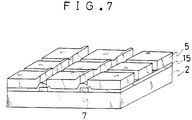
- Fig. 7 is a perspective view showing the schematic structure of a substrate according to a sixth embodiment of the present invention.
- a low-resistance conductive film 7 is formed on a translucent substrate.
- Dot electrodes 5 are formed so as to electrically come in contact with the low-resistance conductive film 7 through an insulating film 15 at a column or row on one side.
- the structure of the present embodiment is the same as that of Embodiment 4 except for the foregoing. According to the liquid crystal display of the present embodiment, display characteristics having a good contrast can be obtained in similar to Embodiments 4 and 5.
- molybdenum is used for the low-resistance conductive film. Even if aluminum, titanium, tantalum or the like is used in place of molybdenum, the same results can be obtained. In addition, even if Al2O3, ZnO, Y2O3, SiO2, SiNx or the like is used for the insulating film 15 in place of Ta2O5, the same results can be obtained.
- the low-resistance conductive films are provided so as to electrically connect a plurality of dot electrodes arranged in a matrix in the row or column direction. Consequently, the low-resistance conductive film formed between the adjacent dot electrodes is positioned lower by the thickness of the dot electrode than the height of the low-resistance conductive film on the dot electrode. A cell is produced such that the low-resistance conductive film between the adjacent dot electrodes is opposed to the low-resistance conductive film on the opposite translucent substrate. Consequently, there can be reduced a possibility that the electric contact between the translucent substrates is caused. Furthermore, the thickness of the low-resistance conductive film can be increased. In addition, the width of the low-resistance conductive film can be reduced. Thus, the active aperture can be prevented from being decreased sharply.
Landscapes
- Physics & Mathematics (AREA)
- Nonlinear Science (AREA)
- Geometry (AREA)
- Mathematical Physics (AREA)
- Chemical & Material Sciences (AREA)
- Crystallography & Structural Chemistry (AREA)
- General Physics & Mathematics (AREA)
- Optics & Photonics (AREA)
- Liquid Crystal (AREA)
- Devices For Indicating Variable Information By Combining Individual Elements (AREA)
Applications Claiming Priority (2)
| Application Number | Priority Date | Filing Date | Title |
|---|---|---|---|
| JP14823/91 | 1991-01-14 | ||
| JP3014823A JP2622033B2 (ja) | 1991-01-14 | 1991-01-14 | 液晶表示装置 |
Publications (3)
| Publication Number | Publication Date |
|---|---|
| EP0495632A2 true EP0495632A2 (fr) | 1992-07-22 |
| EP0495632A3 EP0495632A3 (en) | 1993-01-20 |
| EP0495632B1 EP0495632B1 (fr) | 1996-03-13 |
Family
ID=11871763
Family Applications (1)
| Application Number | Title | Priority Date | Filing Date |
|---|---|---|---|
| EP92300315A Expired - Lifetime EP0495632B1 (fr) | 1991-01-14 | 1992-01-14 | Afficheur à cristal liquide |
Country Status (5)
| Country | Link |
|---|---|
| US (1) | US5274483A (fr) |
| EP (1) | EP0495632B1 (fr) |
| JP (1) | JP2622033B2 (fr) |
| CA (1) | CA2058902C (fr) |
| DE (1) | DE69208898T2 (fr) |
Families Citing this family (5)
| Publication number | Priority date | Publication date | Assignee | Title |
|---|---|---|---|---|
| GB9006919D0 (en) * | 1990-03-28 | 1990-05-23 | Panther Giles | Paging receiver |
| US5753937A (en) * | 1994-05-31 | 1998-05-19 | Casio Computer Co., Ltd. | Color liquid crystal display device having a semitransparent layer on the inner surface of one of the substrates |
| US5777710A (en) * | 1995-04-28 | 1998-07-07 | Canon Kabushiki Kaisha | Electrode substrate, making the same, liquid crystal device provided therewith, and making the same |
| JP2000321600A (ja) * | 1999-05-13 | 2000-11-24 | Internatl Business Mach Corp <Ibm> | 液晶表示装置及びこれの製造方法 |
| JP4783890B2 (ja) * | 2000-02-18 | 2011-09-28 | 株式会社 日立ディスプレイズ | 液晶表示装置 |
Family Cites Families (19)
| Publication number | Priority date | Publication date | Assignee | Title |
|---|---|---|---|---|
| JPS57161882A (en) * | 1981-03-31 | 1982-10-05 | Hitachi Ltd | Display body panel |
| US4824213A (en) * | 1983-12-16 | 1989-04-25 | Citizen Watch Co., Ltd. | Liquid crystal display having opaque portions on the electrodes |
| JPS60249120A (ja) * | 1984-05-24 | 1985-12-09 | Citizen Watch Co Ltd | 液晶表示素子 |
| JPS6125125A (ja) * | 1984-07-13 | 1986-02-04 | Sharp Corp | 液晶表示素子 |
| JPH0766452B2 (ja) * | 1984-08-30 | 1995-07-19 | カシオ計算機株式会社 | 図形データ入力装置 |
| JPS61210325A (ja) * | 1985-03-15 | 1986-09-18 | Hitachi Ltd | 液晶表示素子 |
| JPH0685032B2 (ja) * | 1985-10-17 | 1994-10-26 | キヤノン株式会社 | カイラルスメクティック液晶素子 |
| JPS62121424A (ja) * | 1985-11-22 | 1987-06-02 | Canon Inc | 液晶セル |
| DE3685632T2 (de) * | 1985-11-26 | 1993-01-21 | Canon Kk | Optische modulationsvorrichtung und verfahren zu deren ansteuerung. |
| US4712874A (en) * | 1985-12-25 | 1987-12-15 | Canon Kabushiki Kaisha | Ferroelectric liquid crystal device having color filters on row or column electrodes |
| US4906072A (en) * | 1986-10-09 | 1990-03-06 | Canon Kabushiki Kaisha | Display apparatus and driving method for providing an uniform potential to the electrodes |
| US4859036A (en) * | 1987-05-15 | 1989-08-22 | Canon Kabushiki Kaisha | Device plate having conductive films selected to prevent pin-holes |
| JP2683032B2 (ja) * | 1988-05-06 | 1997-11-26 | キヤノン株式会社 | 液晶素子 |
| US5000545A (en) * | 1987-05-28 | 1991-03-19 | Canon Kabushiki Kaisha | Liquid crystal device with metal electrode partially overlying transparent electrode |
| JPH01179915A (ja) * | 1988-01-11 | 1989-07-18 | Canon Inc | 液晶素子 |
| JP2537951B2 (ja) * | 1988-02-25 | 1996-09-25 | 松下電器産業株式会社 | 液晶ライトバルブ光学装置 |
| JP2694229B2 (ja) * | 1988-03-07 | 1997-12-24 | 株式会社 半導体エネルギー研究所 | 電気光学装置用電極の作製方法 |
| US5132816A (en) * | 1989-02-02 | 1992-07-21 | Sharp Kabushiki Kaisha | Ferroelectric liquid crystal device and method of manufacturing the same |
| US5084778A (en) * | 1989-12-26 | 1992-01-28 | General Electric Company | Electrode structure for removing field-induced disclination lines in a phase control type of liquid crystal device |
-
1991
- 1991-01-14 JP JP3014823A patent/JP2622033B2/ja not_active Expired - Lifetime
-
1992
- 1992-01-07 CA CA002058902A patent/CA2058902C/fr not_active Expired - Fee Related
- 1992-01-14 EP EP92300315A patent/EP0495632B1/fr not_active Expired - Lifetime
- 1992-01-14 DE DE69208898T patent/DE69208898T2/de not_active Expired - Fee Related
- 1992-01-14 US US07/820,273 patent/US5274483A/en not_active Expired - Lifetime
Also Published As
| Publication number | Publication date |
|---|---|
| CA2058902A1 (fr) | 1992-07-15 |
| DE69208898D1 (de) | 1996-04-18 |
| CA2058902C (fr) | 1996-04-09 |
| US5274483A (en) | 1993-12-28 |
| JP2622033B2 (ja) | 1997-06-18 |
| DE69208898T2 (de) | 1996-08-14 |
| EP0495632B1 (fr) | 1996-03-13 |
| JPH04241324A (ja) | 1992-08-28 |
| EP0495632A3 (en) | 1993-01-20 |
Similar Documents
| Publication | Publication Date | Title |
|---|---|---|
| US7202498B2 (en) | Liquid crystal display, thin film transistor array panel therefor, and manufacturing method thereof | |
| US8253913B2 (en) | Liquid crystal display and thin film transistor array panel therefor | |
| US8040479B2 (en) | Liquid crystal display and thin film transistor array panel therefor | |
| US4728176A (en) | Ferroelectric liquid crystal device with metallic auxiliary electrodes provided adjacent to the transparent electrodes | |
| US7292303B2 (en) | Liquid crystal display and panel therefor including regular and successive regular domain defining members | |
| EP0008816B1 (fr) | Dispositif d'affichage à cristal liquide | |
| US20040233343A1 (en) | Liquid crystal display and thin film transistor array panel therefor | |
| US5161043A (en) | Method of forming liquid crystal display device with molybdenum shading layer over ITO electrodes | |
| EP0083822B1 (fr) | Dispositif d'affichage à cristal liquide | |
| JPH06214220A (ja) | 液晶表示装置 | |
| EP0495632B1 (fr) | Afficheur à cristal liquide | |
| CA2012391C (fr) | Dispositif d'affichage a cristaux liquides | |
| US5227899A (en) | Liquid crystal display device with low resistance film separated from one of two adjacent electrodes by an insulating film | |
| JPH09127494A (ja) | 液晶表示装置およびその製造方法 | |
| US7755734B2 (en) | Liquid crystal display and thin film transistor array panel therefor | |
| KR100247110B1 (ko) | 전기 광학 장치 | |
| US20060023151A1 (en) | Liquid crystal display and panel therefor | |
| JP2535414B2 (ja) | 液晶表示装置 | |
| US5231526A (en) | Liquid crystal display device with two insulating films, the second in only non-pixel areas | |
| JP3052361B2 (ja) | アクティブマトリクス液晶表示装置とその製造方法 | |
| JP2654661B2 (ja) | 電気光学表示装置 | |
| JPH11194323A (ja) | 液晶表示素子およびその駆動方法 | |
| JPH06130420A (ja) | 液晶表示装置 | |
| JPH03122622A (ja) | 薄膜二端子素子型アクティブマトリクス液晶表示装置及びその製造方法 | |
| JPH0535411B2 (fr) |
Legal Events
| Date | Code | Title | Description |
|---|---|---|---|
| PUAI | Public reference made under article 153(3) epc to a published international application that has entered the european phase |
Free format text: ORIGINAL CODE: 0009012 |
|
| AK | Designated contracting states |
Kind code of ref document: A2 Designated state(s): DE FR GB NL |
|
| PUAL | Search report despatched |
Free format text: ORIGINAL CODE: 0009013 |
|
| AK | Designated contracting states |
Kind code of ref document: A3 Designated state(s): DE FR GB NL |
|
| 17P | Request for examination filed |
Effective date: 19930226 |
|
| 17Q | First examination report despatched |
Effective date: 19941007 |
|
| GRAA | (expected) grant |
Free format text: ORIGINAL CODE: 0009210 |
|
| AK | Designated contracting states |
Kind code of ref document: B1 Designated state(s): DE FR GB NL |
|
| REF | Corresponds to: |
Ref document number: 69208898 Country of ref document: DE Date of ref document: 19960418 |
|
| ET | Fr: translation filed | ||
| PLBE | No opposition filed within time limit |
Free format text: ORIGINAL CODE: 0009261 |
|
| 26N | No opposition filed | ||
| REG | Reference to a national code |
Ref country code: GB Ref legal event code: IF02 |
|
| PGFP | Annual fee paid to national office [announced via postgrant information from national office to epo] |
Ref country code: FR Payment date: 20020110 Year of fee payment: 11 |
|
| PGFP | Annual fee paid to national office [announced via postgrant information from national office to epo] |
Ref country code: GB Payment date: 20020116 Year of fee payment: 11 |
|
| PGFP | Annual fee paid to national office [announced via postgrant information from national office to epo] |
Ref country code: NL Payment date: 20020131 Year of fee payment: 11 |
|
| PGFP | Annual fee paid to national office [announced via postgrant information from national office to epo] |
Ref country code: DE Payment date: 20020212 Year of fee payment: 11 |
|
| PG25 | Lapsed in a contracting state [announced via postgrant information from national office to epo] |
Ref country code: GB Free format text: LAPSE BECAUSE OF NON-PAYMENT OF DUE FEES Effective date: 20030114 |
|
| PG25 | Lapsed in a contracting state [announced via postgrant information from national office to epo] |
Ref country code: NL Free format text: LAPSE BECAUSE OF NON-PAYMENT OF DUE FEES Effective date: 20030801 Ref country code: DE Free format text: LAPSE BECAUSE OF NON-PAYMENT OF DUE FEES Effective date: 20030801 |
|
| GBPC | Gb: european patent ceased through non-payment of renewal fee | ||
| PG25 | Lapsed in a contracting state [announced via postgrant information from national office to epo] |
Ref country code: FR Free format text: LAPSE BECAUSE OF NON-PAYMENT OF DUE FEES Effective date: 20030930 |
|
| NLV4 | Nl: lapsed or anulled due to non-payment of the annual fee |
Effective date: 20030801 |
|
| REG | Reference to a national code |
Ref country code: FR Ref legal event code: ST |