EP0496171A2 - Bistabile integrierte Halbleiterschaltung - Google Patents
Bistabile integrierte Halbleiterschaltung Download PDFInfo
- Publication number
- EP0496171A2 EP0496171A2 EP91312097A EP91312097A EP0496171A2 EP 0496171 A2 EP0496171 A2 EP 0496171A2 EP 91312097 A EP91312097 A EP 91312097A EP 91312097 A EP91312097 A EP 91312097A EP 0496171 A2 EP0496171 A2 EP 0496171A2
- Authority
- EP
- European Patent Office
- Prior art keywords
- input
- terminal
- output
- input terminal
- gate
- Prior art date
- Legal status (The legal status is an assumption and is not a legal conclusion. Google has not performed a legal analysis and makes no representation as to the accuracy of the status listed.)
- Granted
Links
- 239000004065 semiconductor Substances 0.000 title claims abstract description 21
- 239000000872 buffer Substances 0.000 claims abstract description 77
- 238000010586 diagram Methods 0.000 description 37
- 239000002131 composite material Substances 0.000 description 11
- 229910001218 Gallium arsenide Inorganic materials 0.000 description 3
- 230000001934 delay Effects 0.000 description 3
- 230000000694 effects Effects 0.000 description 2
- 238000012986 modification Methods 0.000 description 2
- 230000004048 modification Effects 0.000 description 2
- 230000002411 adverse Effects 0.000 description 1
- 231100000989 no adverse effect Toxicity 0.000 description 1
- 230000000717 retained effect Effects 0.000 description 1
- 230000000630 rising effect Effects 0.000 description 1
- 238000004904 shortening Methods 0.000 description 1
Images





Classifications
-
- H—ELECTRICITY
- H03—ELECTRONIC CIRCUITRY
- H03K—PULSE TECHNIQUE
- H03K3/00—Circuits for generating electric pulses; Monostable, bistable or multistable circuits
- H03K3/01—Details
- H03K3/012—Modifications of generator to improve response time or to decrease power consumption
-
- H—ELECTRICITY
- H03—ELECTRONIC CIRCUITRY
- H03K—PULSE TECHNIQUE
- H03K19/00—Logic circuits, i.e. having at least two inputs acting on one output; Inverting circuits
-
- H—ELECTRICITY
- H03—ELECTRONIC CIRCUITRY
- H03K—PULSE TECHNIQUE
- H03K3/00—Circuits for generating electric pulses; Monostable, bistable or multistable circuits
- H03K3/02—Generators characterised by the type of circuit or by the means used for producing pulses
- H03K3/027—Generators characterised by the type of circuit or by the means used for producing pulses by the use of logic circuits, with internal or external positive feedback
- H03K3/037—Bistable circuits
-
- H—ELECTRICITY
- H03—ELECTRONIC CIRCUITRY
- H03K—PULSE TECHNIQUE
- H03K3/00—Circuits for generating electric pulses; Monostable, bistable or multistable circuits
- H03K3/02—Generators characterised by the type of circuit or by the means used for producing pulses
- H03K3/027—Generators characterised by the type of circuit or by the means used for producing pulses by the use of logic circuits, with internal or external positive feedback
- H03K3/037—Bistable circuits
- H03K3/0372—Bistable circuits of the primary-secondary type
-
- H—ELECTRICITY
- H03—ELECTRONIC CIRCUITRY
- H03K—PULSE TECHNIQUE
- H03K3/00—Circuits for generating electric pulses; Monostable, bistable or multistable circuits
- H03K3/02—Generators characterised by the type of circuit or by the means used for producing pulses
- H03K3/353—Generators characterised by the type of circuit or by the means used for producing pulses by the use, as active elements, of field-effect transistors with internal or external positive feedback
- H03K3/356—Bistable circuits
Definitions
- This invention relates to a semiconductor integrated circuit composed of flip-flops, which receives data with the timing of a clock signal and retains it.
- Conventional data latch circuits are constructed as shown in Fig. 1A, for example. They are composed primarily of flip-flops using NOR gates. Specifically, the data latch circuit is made up of NOR gates G101 and G102 constituting a flip-flop, a NOR gate G201 serving as an input gate that transfers data D to one input terminal of the flip-flop under the control of clock CK supplied to one input terminal of this gate, and an inverter I101 that inverts clock CK and supplies it to the other input terminal of the flip-flop.
- an inverter buffer I102 is provided as an output buffer as shown Fig. 1B.
- data taken in on clock has to pass through three stages of gate G101, gate G102, and inverter buffer I102 before it reaches the output terminal. This delays the data transfer between the input and output in the data latch circuit.
- Fig. 1C shows another conventional flip-flop circuit, which is composed of NOR gates G101 and G102 constituting a flip-flop stage, AND gates G501 and G502 serving as input gates, and inverter buffers I103 and I104 serving as output buffers.
- the object of the present invention is to provide an improved semiconductor integrated circuit, particularly a flip-flop-based semiconductor integrated circuit capable of high-speed operation.
- a semiconductor integrated circuit comprising: a flip-flop having input terminal means and output terminal means; at least one input gate means having output terminal means connected to the input terminal means, which supplies data to this input terminal under the control of clock; and at least one output buffer means the input terminal means of which is connected to the output terminal means of the flip-flop to receive the output signal of the flip-flop and which is connected to the output terminal means of the input gate means to receive the data from the input gate means to provide an advance read function.
- the output buffer is provided with an advance read function, thereby eliminating a delay due to two stages of gates of the flip-flop in transferring data to the output terminal.
- This approach has no adverse effect on the data retaining function of the flip-flop stage. Consequently, the present invention provides various types of flip-flop circuits and data latch circuits with very small data delays.
- Fig. 3 is a block diagram for a first embodiment of the RS flip-flop circuit having an input gate according to the present invention.
- the set input terminal S and reset input terminal R of an RS flip-flop 100 are provided respectively with input gates 200A and 200B, which transfer input data under the control of clock CK.
- the set output terminal Q and reset output terminal /Q are provided with output buffers 300B and 300A, respectively.
- the output buffer 300B is supplied with the data from the set output terminal Q and the data supplied to the set input terminal S. That is, the data to the set input terminal S is supplied to the output buffer 300B prior being transferred through the flip-flop 100, to provide the buffer with an advance read function.
- the output buffer 300A like the output buffer 300B, is supplied with the data from the reset output terminal /Q and the data supplied to the reset input terminal R.
- Fig. 4 is a circuit diagram for the flip-flop circuit of Fig. 3.
- the RS flip-flop 100 is made up of two NOR gates G101 and G102.
- the input gates 200A and 200B are composed of NOR gates G201 and G202, respectively.
- the output buffer 300A and 300B are composed of NOR gates G301 and G302.
- One NOR gate G301 of the output buffer stage is connected to the output node N3 of the flip-flop stage and the input node N2.
- the other NOR gate G302 of the output buffer stage is connected to the output node N4 of the flip-flop stage and the input node N1.
- Fig. 5 is a timing chart for explaining the operation of the flip-flop circuit of Fig. 4. It is assumed that in the initial state, clock CK is a "1", data A a “0", data /A a "1", nodes N1 and N2 a “0", N3 a “1", N4 a “0", output Q1 a "1", and output /Q1 a "0".
- the change of clock CK from "1" to "0” causes node N1 to change from "0" to "1”.
- This change at node N1 then causes the voltage at the output node N3 of NOR gate G101 to fall. This falling voltage at the output node N3 in turn causes the voltage at the output node N4 of NOR gate G102 to rise.
- Fig. 6 is a circuit diagram for a modification of the flip-flop circuit of Fig. 4.
- AND gates G501 and G502 replace the NOR gates G201 and G202 constituting the input gate of Fig. 4.
- the AND gate G501 and G502 may be such as source-follower AND gates.
- Fig. 7 is a block diagram for a second embodiment of the RS flip-flop circuit having an input gate according to the present invention.
- input gates 200C and 200D are provided to give the output buffers 300A and 300B an advance read function.
- the composite gate arrangement of the input gates 200A and 200B and RS flip-flop 100 is useful particularly in cases where the set input terminal S and reset input terminal R cannot be connected directly to the output buffers 300B and 300A.
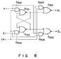
- Fig. 8 is a circuit diagram for the RS flip-flop circuit of Fig. 7.
- NOR gates G101 and G102 constitute the RS flip-flop circuit 100.
- AND gates G503 and G504 are combined with NOR gates G101 and G102, respectively, to form composite gates.
- the output buffer section is also constructed to form a composite gate arrangement of AND and NOR elements.
- FIG. 9A illustrates an equivalent circuit of gate level
- Fig. 9B shows a circuit diagram for the Fig. 9A circuit constructed of MESFETs
- Fig. 9C depicts a circuit diagram for Fig. 9A circuit constructed of CMOS circuits.
- Figs. 10 to 16 illustrate embodiments where the present invention is applied to a data latch circuit.
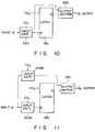
- Fig. 10 is a block diagram for a first embodiment of the data latch circuit according to the present invention.
- a flip-flop 150 for latching data has the data input terminal D, the input terminal for clock CK2, and the output terminal Q.
- the data input terminal D is connected to an input gate 200 that transfers input data under the control of clock CK1.
- the data output terminal Q is connected to an output buffer 300.
- the output buffer 300 is provided with an advance read function that allows the input data to be supplied directly to this buffer before the input passing through the data-latch flip-flop 150. Therefore, as with the above embodiment, the present embodiment provides the output without introducing a delay due to two stages of gates of the data-latch flip-flop 150.
- Fig. 11 is a block diagram for a second embodiment of the data latch circuit according to the present invention.
- another input gate 200B is provided in parallel with the input gate 200A to give the output buffer 300 an advance read function.
- the present embodiment like the embodiment explained in Fig. 7, is useful for composite gate arrangements.
- Fig. 12 is a block diagram for a third embodiment of the data latch circuit according to the present invention.
- the data latch circuit of Fig. 12 is made up of a NOR gate G211 forming the input gate stage 210, NOR gates G111 and G112 constituting a flip-flop stage 110, and a NOR gate G311 forming the output buffer stage 310.
- the clock CK is supplied directly to the NOR gate G211 of the input gate stage 210, and at the same time, is supplied via an inverter gate I111 to the NOR gate G112 of the flip-flop stage.
- the signal at the output node of the input gate stage 210 is supplied to the NOR gate G311 of the output buffer 310 to provide an advance read function.
- Fig. 13 is a block diagram for a fourth embodiment of the data latch circuit according to the present invention.
- the data latch circuit of Fig. 13 is composed of a NAND gate G441 forming the input gate stage 220, NAND gates G401 and G402 constituting the flip-flop stage 120, and a NAND gate G451 forming the output buffer stage 320.
- the clock CK is supplied directly to the NAND gate G441 of the input gate stage 220, and at the same time, is supplied via the inverter gate I111 to the NOR gate G402 of the flip-flop stage.
- the present embodiment allows the signal at the output node of the input gate stage 220 to be supplied to the NAND gate G451 of the output buffer 320 to provide an advance read function.
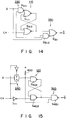
- Fig. 14 is a block diagram for a fifth embodiment of the data latch circuit according to the present invention.
- the flip-flop stage 110 is made up of NOR gates G111 and G112.
- the NOR gate G111 and an AND gate G511 forming the input gate stage 230 are combined to form an AND-to-NOR composite gate arrangement.
- the output buffer stage 330 is made up of the NOR gate G311.
- the NOR gate G311 and an AND gate G512 are combined to form a composite gate arrangement to provide the output buffer 330 with an advance read function.
- Fig. 15 is a block diagram for a sixth embodiment of the data latch circuit according to the present invention.
- the input gate stage 220 of Fig. 13 is constructed of a CMOS transfer gate 240.
- the resistor 400 is designed to present enough resistance for the output node of the transfer gate 220 to go to the "1" level only when the transfer gate 220 turns off.
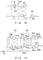
- Fig. 16 is a block diagram for a seventh embodiment of the data latch circuit according to the present invention.
- the input gate stage 230 of Fig. 14 is constructed of a CMOS transfer gate 240.
- the resistor 400 is designed to present enough resistance for the output node of the transfer gate 230 to go to the "0" level only when the transfer gate turns off, and to maintain the node potential.
- the data latch circuits shown in Figs. 10 to 16 like the above-described embodiments, eliminate the effects of internal delay and enable high speed operation.
- Fig. 17 is a circuit diagram for a first embodiment of the master-slave flip-flop circuit according to the present invention.
- the master flip-flop stage 130 is composed of NAND gates G421 and G422 constituting a flip-flop and OR gates G351 and G352 forming transfer gates, all of which are integrated into an OR-to-NAND composite arrangement.
- the slave flip-flop stage 140 is composed of NOR gates G121 and G121 constituting a flip-flop and AND gates G521 and G522 forming transfer gates, all of which are integrated into a NAND-to-NOR composite arrangement.
- the output buffers 340A and 340B each consist of AND-to-NOR composite gates, into which NOR gates G321 and G322 and AND gates G523 and G524 for providing an advance read function are integrated, respectively.
- the AND gates G523 and G524 allow a change in the signal at the output node of the master flip-flop stage 130 to appear at the output buffers 340A and 340B as a change in the output, thereby shortening data delay.
- Fig. 18 is a circuit diagram for a second embodiment of the master-slave flip-flop circuit according to the present invention.
- the master stage is composed of the master flip-flop 110 consisting of NOR gates G123 and G124 and a separate transfer gate 500 consisting of NOR gates G201 and G222.
- Fig. 19 is a circuit diagram for a third embodiment of the master-slave flip-flop circuit according to the present invention.
- the master-slave flip-flop circuit of Fig. 18 is modified in that the slave stage is also composed of the flip-flop 150 consisting of NOR gates G121 and G122 and a separate transfer gate 510 consisting of NAND gates G423 and G424.
- the output buffers 310A and 310B consist only of NOR gates G321 and G322, respectively.
- the output nodes of the NAND gates G423 and G424 of the transfer gate stage 510 are connected to the output buffers 310B and 310A, respectively, to provide these buffers with an advance read function.
- Fig. 20 is a circuit diagram for a fourth embodiment of the master-slave flip-flop circuit according to the present invention.
- the NAND gates of the transfer gate stage 510 of the master-slave flip-flop circuit of Fig. 19 is replaced by NOR gates G125 and G126, which forms the transfer gate stage 520.
- Fig. 21 is an embodiment of the D flip-flop according to the present invention.
- the input gate stage 240 is composed of NOR gates G231, G232, G234, and G235
- the flip-flop stage 110 is made up of NOR gates G131 and G132
- the output buffers 310A and 310B consist of NOR gates G331 and G332, respectively.
- This D flip-flop differs from ordinary D flip-flops in that the output nodes of the input gate stage 240 are connected to the output buffers 310A and 310B to provide these buffers with an advance read function. Consequently, this embodiment also achieves shorter data delay.
Landscapes
- Physics & Mathematics (AREA)
- Engineering & Computer Science (AREA)
- Computer Hardware Design (AREA)
- Computing Systems (AREA)
- General Engineering & Computer Science (AREA)
- Mathematical Physics (AREA)
- Logic Circuits (AREA)
Applications Claiming Priority (2)
| Application Number | Priority Date | Filing Date | Title |
|---|---|---|---|
| JP25549/91 | 1991-01-25 | ||
| JP3025549A JPH04250712A (ja) | 1991-01-25 | 1991-01-25 | 半導体集積回路 |
Publications (3)
| Publication Number | Publication Date |
|---|---|
| EP0496171A2 true EP0496171A2 (de) | 1992-07-29 |
| EP0496171A3 EP0496171A3 (en) | 1993-12-22 |
| EP0496171B1 EP0496171B1 (de) | 1997-03-05 |
Family
ID=12169047
Family Applications (1)
| Application Number | Title | Priority Date | Filing Date |
|---|---|---|---|
| EP91312097A Expired - Lifetime EP0496171B1 (de) | 1991-01-25 | 1991-12-31 | Bistabile integrierte Halbleiterschaltung |
Country Status (5)
| Country | Link |
|---|---|
| US (1) | US5373200A (de) |
| EP (1) | EP0496171B1 (de) |
| JP (1) | JPH04250712A (de) |
| KR (1) | KR950009085B1 (de) |
| DE (1) | DE69124981T2 (de) |
Cited By (1)
| Publication number | Priority date | Publication date | Assignee | Title |
|---|---|---|---|---|
| FR2727783A1 (fr) * | 1994-12-05 | 1996-06-07 | Suisse Electronique Microtech | Element de memoire statique du type bascule latch |
Families Citing this family (8)
| Publication number | Priority date | Publication date | Assignee | Title |
|---|---|---|---|---|
| JPH0548399A (ja) * | 1991-08-08 | 1993-02-26 | Fujitsu Ltd | 半導体装置 |
| US5656962A (en) * | 1994-11-30 | 1997-08-12 | Intel Corporation | Master-slave flip-flop circuit with bypass |
| EP0773627A1 (de) * | 1995-11-07 | 1997-05-14 | STMicroelectronics S.r.l. | Flipflop-Schaltung |
| DE19601370C1 (de) * | 1996-01-16 | 1997-06-12 | Siemens Ag | Statische Halteglieder mit einphasigem Steuersignal |
| DE10320793B4 (de) * | 2003-04-30 | 2005-04-21 | Infineon Technologies Ag | Schaltungs-Einrichtung, insbesondere Latch- oder Phasen-Detektor-Einrichtung |
| JP5807333B2 (ja) * | 2011-01-27 | 2015-11-10 | ソニー株式会社 | ディレイラッチ回路、および、ディレイフリップフロップ |
| CN104658508B (zh) * | 2015-03-24 | 2017-06-09 | 京东方科技集团股份有限公司 | 一种移位寄存器单元、栅极驱动电路及显示装置 |
| CN104835443B (zh) * | 2015-06-03 | 2017-09-26 | 京东方科技集团股份有限公司 | 一种移位寄存单元、栅极驱动电路和显示装置 |
Family Cites Families (10)
| Publication number | Priority date | Publication date | Assignee | Title |
|---|---|---|---|---|
| US4282488A (en) * | 1979-09-17 | 1981-08-04 | Gte Automatic Electric Labs Inc. | Noise eliminator circuit |
| US4314164A (en) * | 1979-11-05 | 1982-02-02 | Gte Automatic Electric Labs Inc. | Computer channel access circuit for multiple input-output devices |
| DE3044835C2 (de) * | 1980-11-28 | 1986-04-03 | Standard Elektrik Lorenz Ag, 7000 Stuttgart | Digitaler Phasendetektor |
| US4475049A (en) * | 1981-05-07 | 1984-10-02 | Smith Robert E | Redundant serial communication circuit |
| US4591737A (en) * | 1982-12-13 | 1986-05-27 | Advanced Micro Devices, Inc. | Master-slave multivibrator with improved metastable response characteristic |
| JPS60134620A (ja) * | 1983-12-23 | 1985-07-17 | Hitachi Ltd | D型フリツプフロツプ |
| NL8501887A (nl) * | 1985-07-01 | 1987-02-02 | Oce Nederland Bv | Fasedetector. |
| US4814726A (en) * | 1987-08-17 | 1989-03-21 | National Semiconductor Corporation | Digital phase comparator/charge pump with zero deadband and minimum offset |
| US4873456A (en) * | 1988-06-06 | 1989-10-10 | Tektronix, Inc. | High speed state machine |
| US5150385A (en) * | 1990-12-28 | 1992-09-22 | Texas Instruments Incorporated | Synchronized pulsed look-ahead circuit and method |
-
1991
- 1991-01-25 JP JP3025549A patent/JPH04250712A/ja active Pending
- 1991-12-31 EP EP91312097A patent/EP0496171B1/de not_active Expired - Lifetime
- 1991-12-31 DE DE69124981T patent/DE69124981T2/de not_active Expired - Fee Related
-
1992
- 1992-01-24 KR KR1019920000991A patent/KR950009085B1/ko not_active Expired - Fee Related
-
1994
- 1994-03-21 US US08/214,678 patent/US5373200A/en not_active Expired - Lifetime
Cited By (2)
| Publication number | Priority date | Publication date | Assignee | Title |
|---|---|---|---|---|
| FR2727783A1 (fr) * | 1994-12-05 | 1996-06-07 | Suisse Electronique Microtech | Element de memoire statique du type bascule latch |
| EP0720173A1 (de) * | 1994-12-05 | 1996-07-03 | C.S.E.M. Centre Suisse D'electronique Et De Microtechnique Sa | Statischer Speicherbaustein des Flip-Flop-Registertyps |
Also Published As
| Publication number | Publication date |
|---|---|
| KR920015736A (ko) | 1992-08-27 |
| EP0496171B1 (de) | 1997-03-05 |
| EP0496171A3 (en) | 1993-12-22 |
| DE69124981T2 (de) | 1997-07-10 |
| JPH04250712A (ja) | 1992-09-07 |
| US5373200A (en) | 1994-12-13 |
| KR950009085B1 (ko) | 1995-08-14 |
| DE69124981D1 (de) | 1997-04-10 |
Similar Documents
| Publication | Publication Date | Title |
|---|---|---|
| JP3587248B2 (ja) | スキャン用フリップフロップ | |
| US6417711B2 (en) | High speed latch and flip-flop | |
| US4710650A (en) | Dual domino CMOS logic circuit, including complementary vectorization and integration | |
| US6753714B2 (en) | Reducing power and area consumption of gated clock enabled flip flops | |
| US5508648A (en) | Differential latch circuit | |
| CA1266517A (en) | Flip-flop circuit | |
| EP0502732B1 (de) | Impulsgenerator | |
| WO2001009900A2 (en) | High speed latch and flip-flop | |
| US4506167A (en) | High speed logic flip-flop latching arrangements including input and feedback pairs of transmission gates | |
| EP1434122A2 (de) | Vorrichtung und Verfahren zur Wiederherstellung von Zurücksetz- und Taktsignalen sowie ein schnelles digitales System mit einer solche Vorrichtung. | |
| US5760612A (en) | Inertial delay circuit for eliminating glitches on a signal line | |
| WO1993019529A1 (en) | Asynchronous-to-synchronous synchronizers, particularly cmos synchronizers | |
| EP0496171A2 (de) | Bistabile integrierte Halbleiterschaltung | |
| US5767718A (en) | High speed conditional synchronous one shot circuit | |
| JPS61262314A (ja) | Cmos技術による静的双安定フリツプフロツプ回路 | |
| US6445236B1 (en) | Master-slave flip-flop circuit with embedded hold function and method for holding data in a master-slave flip-flop circuit | |
| EP0472426B1 (de) | CMOS-Flipflop-Schaltung | |
| EP2175557B1 (de) | Eingangsschaltung | |
| JP2004064557A (ja) | フリップフロップ回路およびシフトレジスタ | |
| EP0871290A2 (de) | Schaltung zur Unterdrückung von Störsignalen | |
| US5187385A (en) | Latch circuit including filter for metastable prevention | |
| JPH08195650A (ja) | マスタスレーブ方式フリップフロップ回路 | |
| JP4201833B2 (ja) | 非同期動作副回路の動作のタイミングを調節する回路 | |
| US4804864A (en) | Multiphase CMOS toggle flip-flop | |
| EP0330707A1 (de) | Verriegelungsschaltung |
Legal Events
| Date | Code | Title | Description |
|---|---|---|---|
| PUAI | Public reference made under article 153(3) epc to a published international application that has entered the european phase |
Free format text: ORIGINAL CODE: 0009012 |
|
| 17P | Request for examination filed |
Effective date: 19920121 |
|
| AK | Designated contracting states |
Kind code of ref document: A2 Designated state(s): DE FR GB |
|
| PUAL | Search report despatched |
Free format text: ORIGINAL CODE: 0009013 |
|
| AK | Designated contracting states |
Kind code of ref document: A3 Designated state(s): DE FR GB |
|
| 17Q | First examination report despatched |
Effective date: 19950201 |
|
| GRAG | Despatch of communication of intention to grant |
Free format text: ORIGINAL CODE: EPIDOS AGRA |
|
| GRAH | Despatch of communication of intention to grant a patent |
Free format text: ORIGINAL CODE: EPIDOS IGRA |
|
| GRAH | Despatch of communication of intention to grant a patent |
Free format text: ORIGINAL CODE: EPIDOS IGRA |
|
| GRAA | (expected) grant |
Free format text: ORIGINAL CODE: 0009210 |
|
| AK | Designated contracting states |
Kind code of ref document: B1 Designated state(s): DE FR GB |
|
| REF | Corresponds to: |
Ref document number: 69124981 Country of ref document: DE Date of ref document: 19970410 |
|
| ET | Fr: translation filed | ||
| PLBE | No opposition filed within time limit |
Free format text: ORIGINAL CODE: 0009261 |
|
| STAA | Information on the status of an ep patent application or granted ep patent |
Free format text: STATUS: NO OPPOSITION FILED WITHIN TIME LIMIT |
|
| 26N | No opposition filed | ||
| REG | Reference to a national code |
Ref country code: GB Ref legal event code: 746 Effective date: 19980929 |
|
| REG | Reference to a national code |
Ref country code: FR Ref legal event code: D6 |
|
| REG | Reference to a national code |
Ref country code: GB Ref legal event code: IF02 |
|
| PGFP | Annual fee paid to national office [announced via postgrant information from national office to epo] |
Ref country code: FR Payment date: 20021210 Year of fee payment: 12 |
|
| PGFP | Annual fee paid to national office [announced via postgrant information from national office to epo] |
Ref country code: GB Payment date: 20021224 Year of fee payment: 12 |
|
| PG25 | Lapsed in a contracting state [announced via postgrant information from national office to epo] |
Ref country code: GB Free format text: LAPSE BECAUSE OF NON-PAYMENT OF DUE FEES Effective date: 20031231 |
|
| GBPC | Gb: european patent ceased through non-payment of renewal fee |
Effective date: 20031231 |
|
| PG25 | Lapsed in a contracting state [announced via postgrant information from national office to epo] |
Ref country code: FR Free format text: LAPSE BECAUSE OF NON-PAYMENT OF DUE FEES Effective date: 20040831 |
|
| REG | Reference to a national code |
Ref country code: FR Ref legal event code: ST |
|
| PGFP | Annual fee paid to national office [announced via postgrant information from national office to epo] |
Ref country code: DE Payment date: 20061229 Year of fee payment: 16 |
|
| PG25 | Lapsed in a contracting state [announced via postgrant information from national office to epo] |
Ref country code: DE Free format text: LAPSE BECAUSE OF NON-PAYMENT OF DUE FEES Effective date: 20080701 |