EP0496553B1 - Phasenregelkreis mit einer eine Rücksetzschaltung enthaltenden Ladungspumpe - Google Patents
Phasenregelkreis mit einer eine Rücksetzschaltung enthaltenden Ladungspumpe Download PDFInfo
- Publication number
- EP0496553B1 EP0496553B1 EP92300457A EP92300457A EP0496553B1 EP 0496553 B1 EP0496553 B1 EP 0496553B1 EP 92300457 A EP92300457 A EP 92300457A EP 92300457 A EP92300457 A EP 92300457A EP 0496553 B1 EP0496553 B1 EP 0496553B1
- Authority
- EP
- European Patent Office
- Prior art keywords
- charge pump
- output
- pump
- inputs
- reset
- Prior art date
- Legal status (The legal status is an assumption and is not a legal conclusion. Google has not performed a legal analysis and makes no representation as to the accuracy of the status listed.)
- Expired - Lifetime
Links
Images

Classifications
-
- H—ELECTRICITY
- H03—ELECTRONIC CIRCUITRY
- H03L—AUTOMATIC CONTROL, STARTING, SYNCHRONISATION OR STABILISATION OF GENERATORS OF ELECTRONIC OSCILLATIONS OR PULSES
- H03L7/00—Automatic control of frequency or phase; Synchronisation
- H03L7/06—Automatic control of frequency or phase; Synchronisation using a reference signal applied to a frequency- or phase-locked loop
- H03L7/08—Details of the phase-locked loop
- H03L7/085—Details of the phase-locked loop concerning mainly the frequency- or phase-detection arrangement including the filtering or amplification of its output signal
- H03L7/089—Details of the phase-locked loop concerning mainly the frequency- or phase-detection arrangement including the filtering or amplification of its output signal the phase or frequency detector generating up-down pulses
- H03L7/0891—Details of the phase-locked loop concerning mainly the frequency- or phase-detection arrangement including the filtering or amplification of its output signal the phase or frequency detector generating up-down pulses the up-down pulses controlling source and sink current generators, e.g. a charge pump
- H03L7/0895—Details of the current generators
Definitions
- the present invention relates, in general, to charge pump devices for use in phase locked loops and, more particularly, to charge pump devices with reset.
- a charge pump is a device typically used to provide a control signal to a voltage controlled oscillator in a phase locked loop (PLL).
- a phase locked loop operates by comparing the phases of a reference signal and a feedback signal in a phase detector.
- a tri-state phase detector such as the MC4044 manufactured by Motorola Inc. provides an output signal to a voltage controlled oscillator (VCO). If the reference and feedback signals are out of phase, the phase detector will adjust the output of the VCO, either up or down, until the two signals are in phase. This correction is typically accomplished by either charging or discharging a capacitor coupled between ground and the VCO input which acts as a low pass filter.
- phase detector typically does not provide sufficient drive current to achieve an adequate loop bandwidth, it is customary to include a charge pump, or current amplifier.
- the charge pump serves to increase the available drive current thereby increasing the loop bandwidth.
- the phase detector would be reset when the up and down signals contemporaneously appear at the output of their respective charge pump outputs.
- the reset logic of the phase detector is designed only for the phase detector itself and does not accommodate the additional delay from the charge pump. Since there is a finite and unpredictable time required from when the phase detector turns on the charge pump and the time when the output current flows, there will be a "dead zone" if no precautions are taken. If overly conservative measures are taken, usually by employing a time delay in the phase detector reset path, the minimum pulse width at zero phase error will be longer than desired with the result that more loop filtering is required to reduce the output pulse energy to an acceptable level. Doing so will undesirably slow the loop response to a frequency change request. The necessary compromise is never satisfying because of wide variations in processing and operating conditions.
- the invention provides a phase locked loop having a charge pump with reset, comprising:
- the invention provides a charge pump for a phase locked loop comprising:
- a charge pump circuit which has a sensing device to sense when there are contemporaneous up and down signals being produced.
- a reset signal is provided from the sensing device to a latch means which is coupled between the input to the device and the pump. Upon reset, the signals entering the device are blocked from the pump.
- FIG. 1 is a block diagram of a phase locked loop having a charge pump embodying the present invention.
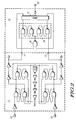
- FIG. 2 is a block diagram of a charge pump embodying the present invention shown in conjunction with a phase detector.
- PLL 10 consists of a phase detector 11, a charge pump 12, a low pass filter (LPF) 13, a voltage controlled oscillator 14, and a feedback divider 15.
- LPF low pass filter
- the phases of a reference signal and a feedback signal are received and compared by phase detector 11. If the signals are out of phase, phase detector 11 will output a signal to charge pump 12 directing that the frequency of the output signal be increased or decreased as appropriate.
- Charge pump 12 as directed by phase detector 11, will then cause a capacitor 16 of filter 13 to either charge, to cause and increase in the output frequency, or discharge, to cause a decrease in the output frequency.
- VCO 14 in response to the voltage provided at its input by LPF 13, will respond by increasing or decreasing the output frequency.
- FIG. 2 a block diagram of a charge pump 12 as coupled to a phase detector 11 is illustrated.
- the two signals to be compared in phase detector 11 are received at nodes 22 and 23. After the phase of the two signals are compared, signals indicating that the frequency of the VCO should be increased and/or decreased are transmitted to charge pump 12 at nodes 24 and 25.
- a reset is determined by sensing the actual output pulse current rather than the input control signal. This will automatically compensate for uncontrollable variations of time delays.
- the up and down outputs of pump 27 are input to a NAND gate 28. When both of the up and down outputs are active, the NAND gate will send a signal to a latching network 29. This will activate the latch and reset charge pump 12. The result will be that the phase detector instruction will be maintained until the desired output current conditions are met.
- phase detector 11 is also provided with its own internal reset provided by NAND gate 30.
- phase detector and charge pump are separate stand alone blocks, each can be a separate block in a CAD design library. The independence of the two blocks significantly simplifies the testing of the parts on an integrated circuit. Furthermore, the structure described here has a dual output capability which allows the phase detector portion to still be used for lock detection and a "low drive" mode, with or without the added charge pump being active.
Landscapes
- Stabilization Of Oscillater, Synchronisation, Frequency Synthesizers (AREA)
- Measuring Phase Differences (AREA)
- Manipulation Of Pulses (AREA)
Claims (10)
- Phasenregelschleife (10) mit einer Ladungspumpe (12) mit Rücksetzung, umfassend:eine Einrichtung (14), die ein Ausgangssignal erzeugt, wobei das Ausgangssignal eine Frequenz aufweist, die als Reaktion auf ein Steuersignal veränderbar ist;eine Einrichtung (15), die das Ausgangssignal teilt, um ein geteiltes Signal bereitzustellen;eine Phasendetektoreinrichtung (11), die eine Phase eines Bezugssignals und eine Phase des geteilten Signals vergleicht und einen ersten und zweiten Ausgang besitzt;wobei die Ladungspumpe (12) einen ersten und zweiten Eingang (24, 25) besitzt, die mit dem ersten bzw. zweiten Ausgang der Phasendetektoreinrichtung (11) verbunden sind, wobei die Ladungspumpe (12) eine Pumpe (27) mit einem ersten und zweiten Eingang und einem ersten und zweiten Ausgang umfaßt, um Aufwärts- und Abwärtssignale zu erzeugen, um dadurch das Steuersignal an einem Ausgang der Ladungspumpe (12) bereitzustellen,dadurch gekennzeichnet, daßdie Ladungspumpe (12) das Steuersignal ansprechend auf ein erstes und zweites internes Signal, die dem ersten und zweiten Eingang der Pumpe (27) zugeführt werden, und entsprechend dem ersten und zweiten Eingang (24, 25) der Ladungspumpe (12) erzeugt, wobei die Ladungspumpe (12) eine Steuereinrichtung (28, 29) enthält, die das erste und zweite interne Signal als Reaktion auf gleichzeitige Aufwärts- und Abwärtssignale, die an dem ersten und zweiten Ausgang der Pumpe (27) erzeugt werden, zurücksetzt, um dadurch die Ladungspumpe (12) zurückzusetzen.
- Phasenregelschleife (10) nach Anspruch 1, bei der die Phasendetektoreinrichtung (11) umfaßt:eine Einrichtung, die ein erstes Stromsignal abtastet, um ein erstes abgetastetes Signal zu erzeugen;eine Einrichtung, die ein zweites Stromsignal abtastet, um ein zweites abgetastetes Signal zu erzeugen, undeine Einrichtung, die als Reaktion auf das erste und zweite abgetastete Signal ein Rücksetzsignal zum Rücksetzen der Phasendetektoreinrichtung (11) erzeugt.
- Phasenregelschleife (10) nach Anspruch 1 oder 2, weiter dadurch gekennzeichnet, daß die Einrichtung (14), die das Ausgangssignal erzeugt, einen spannungsgesteuerten Oszillator (14) umfaßt.
- Phasenregelschleife (10) nach Anspruch 1, 2 oder 3, dadurch gekennzeichnet, daß die Steuereinrichtung (28, 29) umfaßt:eine erste Gattereinrichtung (28) mit einem ersten und zweiten Eingang, die mit dem ersten und zweiten Ausgang der Pumpe (27) verbunden sind, und einem Rücksetzausgang undeine Latch-Einrichtung (29) mit einem ersten und zweiten Eingang, die mit dem ersten und zweiten Eingang der Ladungspumpe (12) verbunden sind, einem ersten und zweiten Ausgang, die mit dem ersten und zweiten Eingang der Pumpe (27) verbunden sind, und einem Rücksetzeingang, der mit dem Rücksetzausgang der ersten Gattereinrichtung verbunden ist.
- Phasenregelschleife (10) nach Anspruch 4, dadurch gekennzeichnet, daß die erste Gattereinrichtung (28) ein NAND-Gatter umfaßt.
- Ladungspumpe (12) für eine Phasenregelschleife (10), umfassend:einen ersten und zweiten Eingang (24, 25);eine Pumpe (27) mit einem ersten und zweiten Eingang und einem ersten und zweiten Ausgang, um Aufwärts- und Abwärtssignale zu erzeugen, um dadurch ein Steuersignal an einem Ausgang der Ladungspumpe (12) bereitzustellen;eine erste Gattereinrichtung (28) mit einem ersten und zweiten Eingang, die mit dem ersten und zweiten Ausgang der Pumpe (27) verbunden sind, und einem Rücksetzausgang,gekennzeichnet durch;eine Latch-Einrichtung (29) mit einem ersten und zweiten Eingang, die mit dem ersten und zweiten Eingang (24, 25) der Ladungspumpe (12) verbunden sind und ein erstes und zweites Stromsignal empfangen, einem ersten und zweiten Ausgang, die mit dem ersten und zweiten Eingang der Pumpe (27) verbunden sind, und einem Rücksetzeingang, der mit dem Rücksetzausgang der ersten Gattereinrichtung (28) verbunden ist und die Latch-Einrichtung (29) als Reaktion auf gleichzeitige Aufwärts- und Abwärtssignale, die an dem ersten und zweiten Ausgang der Pumpe (27) erzeugt werden, aktiviert, um dadurch die Ladungspumpe (12) zurückzusetzen.
- Ladungspumpe nach Anspruch 6, dadurch gekennzeichnet, daß die erste Gattereinrichtung (28) ein NAND-Gatter umfaßt.
- Ladungspumpe (12) nach Anspruch 6 oder 7, bei der die Latch-Einrichtung (29) umfaßt:eine zweite Gattereinrichtung mit einem ersten Eingang, der mit dem ersten Eingang der Latch-Einrichtung (29) verbunden ist, einem zweiten Eingang und einem Ausgang, der mit dem ersten Eingang der Pumpe (27) verbunden ist;eine dritte Gattereinrichtung mit einem ersten Eingang, der mit dem Ausgang der zweiten Gattereinrichtung verbunden ist, einem zweiten Eingang, der mit dem Rücksetzausgang der ersten Gattereinrichtung verbunden ist, und einem Ausgang, der mit dem zweiten Eingang der zweiten Gattereinrichtung verbunden ist;eine vierte Gattereinrichtung mit einem ersten Eingang, der mit dem Rücksetzausgang der ersten Gattereinrichtung verbunden ist, einem zweiten Eingang und einem Ausgang undeine fünfte Gattereinrichtung mit einem ersten Eingang, der mit dem Ausgang der vierten Gattereinrichtung verbunden ist, einem zweiten Eingang, der mit dem zweiten Eingang der Latch-Einrichtung (29) verbunden ist, und einem Ausgang, der mit dem zweiten Eingang der Pumpe (27) und mit dem zweiten Eingang der vierten Gattereinrichtung verbunden ist.
- Ladungspumpe (12) nach Anspruch 8, bei der die zweite, dritte, vierte und fünfte Gattereinrichtung NAND-Gatter sind.
- Phasenregelschleife (10) nach einem der Ansprüche 1 bis 5, bei der die Ladungspumpe (12) wie in einem der Ansprüche 6 bis 9 dargelegt ist.
Applications Claiming Priority (2)
| Application Number | Priority Date | Filing Date | Title |
|---|---|---|---|
| US07/645,170 US5095287A (en) | 1991-01-24 | 1991-01-24 | Phase locked loop having a charge pump with reset |
| US645170 | 1991-01-24 |
Publications (3)
| Publication Number | Publication Date |
|---|---|
| EP0496553A2 EP0496553A2 (de) | 1992-07-29 |
| EP0496553A3 EP0496553A3 (en) | 1992-12-09 |
| EP0496553B1 true EP0496553B1 (de) | 1996-05-01 |
Family
ID=24587900
Family Applications (1)
| Application Number | Title | Priority Date | Filing Date |
|---|---|---|---|
| EP92300457A Expired - Lifetime EP0496553B1 (de) | 1991-01-24 | 1992-01-20 | Phasenregelkreis mit einer eine Rücksetzschaltung enthaltenden Ladungspumpe |
Country Status (4)
| Country | Link |
|---|---|
| US (1) | US5095287A (de) |
| EP (1) | EP0496553B1 (de) |
| JP (1) | JP2778329B2 (de) |
| DE (1) | DE69210263T2 (de) |
Families Citing this family (29)
| Publication number | Priority date | Publication date | Assignee | Title |
|---|---|---|---|---|
| US5339408A (en) * | 1992-12-30 | 1994-08-16 | Digital Equipment Corporation | Method and apparatus for reducing checking costs in fault tolerant processors |
| US5359299A (en) * | 1993-01-21 | 1994-10-25 | Gennum Corporation | High speed and low drift charge pump circuit |
| US5347234A (en) * | 1993-03-26 | 1994-09-13 | International Business Machines Corp. | Digital voltage controlled oscillator |
| US5373255A (en) * | 1993-07-28 | 1994-12-13 | Motorola, Inc. | Low-power, jitter-compensated phase locked loop and method therefor |
| DE4342266C2 (de) * | 1993-12-10 | 1996-10-24 | Texas Instruments Deutschland | Taktgenerator sowie Phasenkomparator zur Verwendung in einem solchen Taktgenerator |
| EP0665650A1 (de) * | 1994-01-31 | 1995-08-02 | STMicroelectronics S.A. | Hochgeschwindigkeitsniederspannungsphasendetektor |
| FR2717019A1 (fr) * | 1994-03-02 | 1995-09-08 | Philips Composants | Dispositif oscillateur verrouillé en phase. |
| KR960006292A (ko) * | 1994-07-28 | 1996-02-23 | 사또 겐이찌로 | 주파수위상비교기 |
| US5495207A (en) * | 1994-08-31 | 1996-02-27 | International Business Machines Corporation | Differential current controlled oscillator with variable load |
| US5513225A (en) * | 1994-08-31 | 1996-04-30 | International Business Machines Corporation | Resistorless phase locked loop circuit employing direct current injection |
| US5525932A (en) * | 1994-08-31 | 1996-06-11 | International Business Machines Corporation | Lock indicator for phase locked loop circuit |
| US5619161A (en) * | 1994-08-31 | 1997-04-08 | International Business Machines Corporation | Diffrential charge pump with integrated common mode control |
| US5491439A (en) * | 1994-08-31 | 1996-02-13 | International Business Machines Corporation | Method and apparatus for reducing jitter in a phase locked loop circuit |
| US5574894A (en) * | 1994-11-03 | 1996-11-12 | Motorola, Inc. | Integrated circuit data processor which provides external sensibility of internal signals during reset |
| SG79917A1 (en) | 1995-04-26 | 2001-04-17 | Canon Kk | Liquid ejecting method with movable member |
| US5828254A (en) * | 1995-06-21 | 1998-10-27 | Sony Corporation | Error regulator circuit for sample and hold phase locked loops |
| JPH09214331A (ja) * | 1995-11-30 | 1997-08-15 | Fujitsu Ltd | Pll周波数シンセサイザ及びその駆動方法 |
| US5833812A (en) * | 1996-02-21 | 1998-11-10 | Hartman; Michael Orban | Low maintenance water distiller |
| US5661419A (en) * | 1996-05-23 | 1997-08-26 | Sun Microsystems, Inc. | Dynamic phase-frequency detector circuit |
| KR19990009178A (ko) * | 1997-07-08 | 1999-02-05 | 윤종용 | 데드 존이 없는 디지탈 위상 동기 루프와 위상 비교 및 전하 펌핑 방법 |
| JPH11127076A (ja) * | 1997-10-21 | 1999-05-11 | Matsushita Electric Ind Co Ltd | フェイズロックループ回路 |
| US6448820B1 (en) * | 1998-11-04 | 2002-09-10 | Altera Corporation | Fast locking phase frequency detector |
| US6605935B2 (en) * | 2001-03-21 | 2003-08-12 | Telefonaktiebolaget L M Ericsson (Publ) | Linear fast-locking digital phase detector |
| DE60209197T2 (de) * | 2002-04-04 | 2006-09-07 | Texas Instruments Inc., Dallas | Phasenregelschleife mit einer Ladungspumpe |
| DE10237120B3 (de) * | 2002-08-13 | 2004-04-15 | Infineon Technologies Ag | Phasendetektor |
| ITMI20030485A1 (it) * | 2003-03-14 | 2004-09-15 | St Microelectronics Srl | Rilevatore di sfasamento perfezionato, particolarmente |
| DE10320793B4 (de) * | 2003-04-30 | 2005-04-21 | Infineon Technologies Ag | Schaltungs-Einrichtung, insbesondere Latch- oder Phasen-Detektor-Einrichtung |
| US20060131484A1 (en) * | 2004-12-17 | 2006-06-22 | Mark Peting | High-dynamic range image sensors |
| US9130575B2 (en) | 2013-03-14 | 2015-09-08 | Samsung Electronics Co., Ltd. | Communication system with charge pump mechanism and method of operation thereof |
Family Cites Families (3)
| Publication number | Priority date | Publication date | Assignee | Title |
|---|---|---|---|---|
| US3714463A (en) * | 1971-01-04 | 1973-01-30 | Motorola Inc | Digital frequency and/or phase detector charge pump |
| JPH0770168B2 (ja) * | 1987-08-17 | 1995-07-31 | 日本電気株式会社 | 磁気ディスク装置用pll回路 |
| US4814726A (en) * | 1987-08-17 | 1989-03-21 | National Semiconductor Corporation | Digital phase comparator/charge pump with zero deadband and minimum offset |
-
1991
- 1991-01-24 US US07/645,170 patent/US5095287A/en not_active Expired - Lifetime
-
1992
- 1992-01-20 EP EP92300457A patent/EP0496553B1/de not_active Expired - Lifetime
- 1992-01-20 DE DE69210263T patent/DE69210263T2/de not_active Expired - Fee Related
- 1992-01-22 JP JP4029880A patent/JP2778329B2/ja not_active Expired - Fee Related
Also Published As
| Publication number | Publication date |
|---|---|
| US5095287A (en) | 1992-03-10 |
| EP0496553A3 (en) | 1992-12-09 |
| EP0496553A2 (de) | 1992-07-29 |
| DE69210263D1 (de) | 1996-06-05 |
| DE69210263T2 (de) | 1996-11-07 |
| JPH0548448A (ja) | 1993-02-26 |
| JP2778329B2 (ja) | 1998-07-23 |
Similar Documents
| Publication | Publication Date | Title |
|---|---|---|
| US5095287A (en) | Phase locked loop having a charge pump with reset | |
| EP0482823B1 (de) | Frequenzsynthesierer mit PLL, der einen Frequenzwechsel des Ausgangs mit hoher Geschwindigkeit ermöglicht | |
| US5822387A (en) | Apparatus for fast phase-locked loop (PLL) frequency slewing during power on | |
| US5257294A (en) | Phase-locked loop circuit and method | |
| US5724007A (en) | Adjustable lock detector for a phase-locked loop circuit | |
| US5838205A (en) | Variable-speed phase-locked loop system with on-the-fly switching and method therefor | |
| US5892380A (en) | Method for shaping a pulse width and circuit therefor | |
| EP0519892B1 (de) | Spannungsgesteuerter Oszillator mit Mehrfachschleife | |
| US5642082A (en) | Loop filter level detection circuit and method | |
| EP0777333B1 (de) | Energiesparende Phasenregelkreisschaltung | |
| US20010053100A1 (en) | Delay-locked loop with binary-coupled capacitor | |
| US7920665B1 (en) | Symmetrical range controller circuit and method | |
| JPH11510664A (ja) | 高速及び高精度の位相ロックループ | |
| KR20050052526A (ko) | 집적된 pll을 구비한 펄스-폭 변조 제어기 | |
| EP0483260B1 (de) | Phasendetektor | |
| US6853252B2 (en) | Phase-lock loop having programmable bandwidth | |
| US4817199A (en) | Phase locked loop having reduced response time | |
| EP0582390B1 (de) | Phasenregelkreis mit zwei Betriebsorten | |
| US5359297A (en) | VCO power-up circuit for PLL and method thereof | |
| US6060953A (en) | PLL response time accelerating system using a frequency detector counter | |
| US4935707A (en) | Current reduction of a synthesizer | |
| US5959478A (en) | Phase-locked loop having improved locking times and a method of operation therefore | |
| HK1009892B (en) | Divider synchronization circuit | |
| JPH0440117A (ja) | Pll回路 | |
| JPH02113726A (ja) | Pll回路 |
Legal Events
| Date | Code | Title | Description |
|---|---|---|---|
| PUAI | Public reference made under article 153(3) epc to a published international application that has entered the european phase |
Free format text: ORIGINAL CODE: 0009012 |
|
| AK | Designated contracting states |
Kind code of ref document: A2 Designated state(s): DE FR GB |
|
| RIN1 | Information on inventor provided before grant (corrected) |
Inventor name: IRWIN, JAME S. Inventor name: MOELLER, DAVID F. |
|
| PUAL | Search report despatched |
Free format text: ORIGINAL CODE: 0009013 |
|
| AK | Designated contracting states |
Kind code of ref document: A3 Designated state(s): DE FR GB |
|
| 17P | Request for examination filed |
Effective date: 19930503 |
|
| 17Q | First examination report despatched |
Effective date: 19930709 |
|
| GRAH | Despatch of communication of intention to grant a patent |
Free format text: ORIGINAL CODE: EPIDOS IGRA |
|
| GRAA | (expected) grant |
Free format text: ORIGINAL CODE: 0009210 |
|
| AK | Designated contracting states |
Kind code of ref document: B1 Designated state(s): DE FR GB |
|
| REF | Corresponds to: |
Ref document number: 69210263 Country of ref document: DE Date of ref document: 19960605 |
|
| ET | Fr: translation filed | ||
| PLBE | No opposition filed within time limit |
Free format text: ORIGINAL CODE: 0009261 |
|
| 26N | No opposition filed | ||
| REG | Reference to a national code |
Ref country code: GB Ref legal event code: 746 Effective date: 19990930 |
|
| REG | Reference to a national code |
Ref country code: FR Ref legal event code: D6 |
|
| REG | Reference to a national code |
Ref country code: GB Ref legal event code: IF02 |
|
| REG | Reference to a national code |
Ref country code: GB Ref legal event code: 732E |
|
| PGFP | Annual fee paid to national office [announced via postgrant information from national office to epo] |
Ref country code: GB Payment date: 20061213 Year of fee payment: 16 |
|
| PGFP | Annual fee paid to national office [announced via postgrant information from national office to epo] |
Ref country code: DE Payment date: 20070131 Year of fee payment: 16 |
|
| PGFP | Annual fee paid to national office [announced via postgrant information from national office to epo] |
Ref country code: FR Payment date: 20070103 Year of fee payment: 16 |
|
| GBPC | Gb: european patent ceased through non-payment of renewal fee |
Effective date: 20080120 |
|
| PG25 | Lapsed in a contracting state [announced via postgrant information from national office to epo] |
Ref country code: DE Free format text: LAPSE BECAUSE OF NON-PAYMENT OF DUE FEES Effective date: 20080801 |
|
| REG | Reference to a national code |
Ref country code: FR Ref legal event code: ST Effective date: 20081029 |
|
| PG25 | Lapsed in a contracting state [announced via postgrant information from national office to epo] |
Ref country code: GB Free format text: LAPSE BECAUSE OF NON-PAYMENT OF DUE FEES Effective date: 20080120 |
|
| PG25 | Lapsed in a contracting state [announced via postgrant information from national office to epo] |
Ref country code: FR Free format text: LAPSE BECAUSE OF NON-PAYMENT OF DUE FEES Effective date: 20080131 |