EP0497592A2 - Nicht-Einkristall-Halbleiteranordnung und Verfahren zur Herstellung - Google Patents
Nicht-Einkristall-Halbleiteranordnung und Verfahren zur Herstellung Download PDFInfo
- Publication number
- EP0497592A2 EP0497592A2 EP92300787A EP92300787A EP0497592A2 EP 0497592 A2 EP0497592 A2 EP 0497592A2 EP 92300787 A EP92300787 A EP 92300787A EP 92300787 A EP92300787 A EP 92300787A EP 0497592 A2 EP0497592 A2 EP 0497592A2
- Authority
- EP
- European Patent Office
- Prior art keywords
- film
- amorphous silicon
- single crystal
- substrate
- transistor
- Prior art date
- Legal status (The legal status is an assumption and is not a legal conclusion. Google has not performed a legal analysis and makes no representation as to the accuracy of the status listed.)
- Ceased
Links
Images





Classifications
-
- H—ELECTRICITY
- H10—SEMICONDUCTOR DEVICES; ELECTRIC SOLID-STATE DEVICES NOT OTHERWISE PROVIDED FOR
- H10P—GENERIC PROCESSES OR APPARATUS FOR THE MANUFACTURE OR TREATMENT OF DEVICES COVERED BY CLASS H10
- H10P14/00—Formation of materials, e.g. in the shape of layers or pillars
- H10P14/20—Formation of materials, e.g. in the shape of layers or pillars of semiconductor materials
- H10P14/38—Formation of materials, e.g. in the shape of layers or pillars of semiconductor materials characterised by treatments done after the formation of the materials
- H10P14/3802—Crystallisation or recrystallisation of non-monocrystalline semiconductor materials, e.g. regrowth
-
- H—ELECTRICITY
- H04—ELECTRIC COMMUNICATION TECHNIQUE
- H04N—PICTORIAL COMMUNICATION, e.g. TELEVISION
- H04N1/00—Scanning, transmission or reproduction of documents or the like, e.g. facsimile transmission; Details thereof
- H04N1/024—Details of scanning heads ; Means for illuminating the original
- H04N1/028—Details of scanning heads ; Means for illuminating the original for picture information pick-up
- H04N1/03—Details of scanning heads ; Means for illuminating the original for picture information pick-up with photodetectors arranged in a substantially linear array
- H04N1/031—Details of scanning heads ; Means for illuminating the original for picture information pick-up with photodetectors arranged in a substantially linear array the photodetectors having a one-to-one and optically positive correspondence with the scanned picture elements, e.g. linear contact sensors
- H04N1/0313—Direct contact pick-up heads, i.e. heads having no array of elements to project the scanned image elements onto the photodectors
-
- H—ELECTRICITY
- H04—ELECTRIC COMMUNICATION TECHNIQUE
- H04N—PICTORIAL COMMUNICATION, e.g. TELEVISION
- H04N1/00—Scanning, transmission or reproduction of documents or the like, e.g. facsimile transmission; Details thereof
- H04N1/024—Details of scanning heads ; Means for illuminating the original
- H04N1/028—Details of scanning heads ; Means for illuminating the original for picture information pick-up
- H04N1/03—Details of scanning heads ; Means for illuminating the original for picture information pick-up with photodetectors arranged in a substantially linear array
- H04N1/031—Details of scanning heads ; Means for illuminating the original for picture information pick-up with photodetectors arranged in a substantially linear array the photodetectors having a one-to-one and optically positive correspondence with the scanned picture elements, e.g. linear contact sensors
- H04N1/0315—Details of scanning heads ; Means for illuminating the original for picture information pick-up with photodetectors arranged in a substantially linear array the photodetectors having a one-to-one and optically positive correspondence with the scanned picture elements, e.g. linear contact sensors using photodetectors and illumination means mounted on separate supports or substrates or mounted in different planes
- H04N1/0316—Details of scanning heads ; Means for illuminating the original for picture information pick-up with photodetectors arranged in a substantially linear array the photodetectors having a one-to-one and optically positive correspondence with the scanned picture elements, e.g. linear contact sensors using photodetectors and illumination means mounted on separate supports or substrates or mounted in different planes illuminating the scanned image elements through the plane of the photodetector, e.g. back-light illumination
-
- H—ELECTRICITY
- H10—SEMICONDUCTOR DEVICES; ELECTRIC SOLID-STATE DEVICES NOT OTHERWISE PROVIDED FOR
- H10D—INORGANIC ELECTRIC SEMICONDUCTOR DEVICES
- H10D30/00—Field-effect transistors [FET]
- H10D30/01—Manufacture or treatment
- H10D30/021—Manufacture or treatment of FETs having insulated gates [IGFET]
- H10D30/031—Manufacture or treatment of FETs having insulated gates [IGFET] of thin-film transistors [TFT]
- H10D30/0312—Manufacture or treatment of FETs having insulated gates [IGFET] of thin-film transistors [TFT] characterised by the gate electrodes
- H10D30/0314—Manufacture or treatment of FETs having insulated gates [IGFET] of thin-film transistors [TFT] characterised by the gate electrodes of lateral top-gate TFTs comprising only a single gate
-
- H—ELECTRICITY
- H10—SEMICONDUCTOR DEVICES; ELECTRIC SOLID-STATE DEVICES NOT OTHERWISE PROVIDED FOR
- H10D—INORGANIC ELECTRIC SEMICONDUCTOR DEVICES
- H10D30/00—Field-effect transistors [FET]
- H10D30/01—Manufacture or treatment
- H10D30/021—Manufacture or treatment of FETs having insulated gates [IGFET]
- H10D30/031—Manufacture or treatment of FETs having insulated gates [IGFET] of thin-film transistors [TFT]
- H10D30/0321—Manufacture or treatment of FETs having insulated gates [IGFET] of thin-film transistors [TFT] comprising silicon, e.g. amorphous silicon or polysilicon
-
- H—ELECTRICITY
- H10—SEMICONDUCTOR DEVICES; ELECTRIC SOLID-STATE DEVICES NOT OTHERWISE PROVIDED FOR
- H10D—INORGANIC ELECTRIC SEMICONDUCTOR DEVICES
- H10D30/00—Field-effect transistors [FET]
- H10D30/60—Insulated-gate field-effect transistors [IGFET]
- H10D30/67—Thin-film transistors [TFT]
- H10D30/6729—Thin-film transistors [TFT] characterised by the electrodes
- H10D30/673—Thin-film transistors [TFT] characterised by the electrodes characterised by the shapes, relative sizes or dispositions of the gate electrodes
- H10D30/6731—Top-gate only TFTs
-
- H—ELECTRICITY
- H10—SEMICONDUCTOR DEVICES; ELECTRIC SOLID-STATE DEVICES NOT OTHERWISE PROVIDED FOR
- H10D—INORGANIC ELECTRIC SEMICONDUCTOR DEVICES
- H10D30/00—Field-effect transistors [FET]
- H10D30/60—Insulated-gate field-effect transistors [IGFET]
- H10D30/67—Thin-film transistors [TFT]
- H10D30/674—Thin-film transistors [TFT] characterised by the active materials
- H10D30/6741—Group IV materials, e.g. germanium or silicon carbide
- H10D30/6743—Silicon
- H10D30/6745—Polycrystalline or microcrystalline silicon
-
- H—ELECTRICITY
- H10—SEMICONDUCTOR DEVICES; ELECTRIC SOLID-STATE DEVICES NOT OTHERWISE PROVIDED FOR
- H10F—INORGANIC SEMICONDUCTOR DEVICES SENSITIVE TO INFRARED RADIATION, LIGHT, ELECTROMAGNETIC RADIATION OF SHORTER WAVELENGTH OR CORPUSCULAR RADIATION
- H10F30/00—Individual radiation-sensitive semiconductor devices in which radiation controls the flow of current through the devices, e.g. photodetectors
- H10F30/20—Individual radiation-sensitive semiconductor devices in which radiation controls the flow of current through the devices, e.g. photodetectors the devices having potential barriers, e.g. phototransistors
- H10F30/21—Individual radiation-sensitive semiconductor devices in which radiation controls the flow of current through the devices, e.g. photodetectors the devices having potential barriers, e.g. phototransistors the devices being sensitive to infrared, visible or ultraviolet radiation
- H10F30/22—Individual radiation-sensitive semiconductor devices in which radiation controls the flow of current through the devices, e.g. photodetectors the devices having potential barriers, e.g. phototransistors the devices being sensitive to infrared, visible or ultraviolet radiation the devices having only one potential barrier, e.g. photodiodes
- H10F30/223—Individual radiation-sensitive semiconductor devices in which radiation controls the flow of current through the devices, e.g. photodetectors the devices having potential barriers, e.g. phototransistors the devices being sensitive to infrared, visible or ultraviolet radiation the devices having only one potential barrier, e.g. photodiodes the potential barrier being a PIN barrier
- H10F30/2235—Individual radiation-sensitive semiconductor devices in which radiation controls the flow of current through the devices, e.g. photodetectors the devices having potential barriers, e.g. phototransistors the devices being sensitive to infrared, visible or ultraviolet radiation the devices having only one potential barrier, e.g. photodiodes the potential barrier being a PIN barrier the devices comprising Group IV amorphous materials
-
- H—ELECTRICITY
- H10—SEMICONDUCTOR DEVICES; ELECTRIC SOLID-STATE DEVICES NOT OTHERWISE PROVIDED FOR
- H10P—GENERIC PROCESSES OR APPARATUS FOR THE MANUFACTURE OR TREATMENT OF DEVICES COVERED BY CLASS H10
- H10P14/00—Formation of materials, e.g. in the shape of layers or pillars
- H10P14/20—Formation of materials, e.g. in the shape of layers or pillars of semiconductor materials
- H10P14/24—Formation of materials, e.g. in the shape of layers or pillars of semiconductor materials using chemical vapour deposition [CVD]
-
- H—ELECTRICITY
- H10—SEMICONDUCTOR DEVICES; ELECTRIC SOLID-STATE DEVICES NOT OTHERWISE PROVIDED FOR
- H10P—GENERIC PROCESSES OR APPARATUS FOR THE MANUFACTURE OR TREATMENT OF DEVICES COVERED BY CLASS H10
- H10P14/00—Formation of materials, e.g. in the shape of layers or pillars
- H10P14/20—Formation of materials, e.g. in the shape of layers or pillars of semiconductor materials
- H10P14/29—Formation of materials, e.g. in the shape of layers or pillars of semiconductor materials characterised by the substrates
- H10P14/2901—Materials
- H10P14/2922—Materials being non-crystalline insulating materials, e.g. glass or polymers
-
- H—ELECTRICITY
- H10—SEMICONDUCTOR DEVICES; ELECTRIC SOLID-STATE DEVICES NOT OTHERWISE PROVIDED FOR
- H10P—GENERIC PROCESSES OR APPARATUS FOR THE MANUFACTURE OR TREATMENT OF DEVICES COVERED BY CLASS H10
- H10P14/00—Formation of materials, e.g. in the shape of layers or pillars
- H10P14/20—Formation of materials, e.g. in the shape of layers or pillars of semiconductor materials
- H10P14/34—Deposited materials, e.g. layers
- H10P14/3402—Deposited materials, e.g. layers characterised by the chemical composition
- H10P14/3404—Deposited materials, e.g. layers characterised by the chemical composition being Group IVA materials
- H10P14/3411—Silicon, silicon germanium or germanium
-
- Y—GENERAL TAGGING OF NEW TECHNOLOGICAL DEVELOPMENTS; GENERAL TAGGING OF CROSS-SECTIONAL TECHNOLOGIES SPANNING OVER SEVERAL SECTIONS OF THE IPC; TECHNICAL SUBJECTS COVERED BY FORMER USPC CROSS-REFERENCE ART COLLECTIONS [XRACs] AND DIGESTS
- Y10—TECHNICAL SUBJECTS COVERED BY FORMER USPC
- Y10S—TECHNICAL SUBJECTS COVERED BY FORMER USPC CROSS-REFERENCE ART COLLECTIONS [XRACs] AND DIGESTS
- Y10S257/00—Active solid-state devices, e.g. transistors, solid-state diodes
- Y10S257/905—Plural dram cells share common contact or common trench
Definitions
- the present invention relates to a non single crystal semiconductor device, in particular, relates to a thin film transistor (TFT) which has a substrate made of glass, and a thin film made of non single crystal silicon deposited on the substrate.
- TFT thin film transistor
- a thin film transistor has been used in an image sensor used in a facsimile device, and/or a liquid crystal display panel.
- a thin film transistor is produced in a non single crystal semiconductor film, which is polycrystal silicon layer deposited on a substrate of quartz or glass.
- a transistor is produced on the substrate through high temperature process up to 900°C.
- a quartz substrate has the disadvantage that the price of the substrate is high, and the high price of the substrate increases the price of a semiconductor device itself.
- a transistor is produced on the substrate through relatively low temperature up to 600°C, because glass is softened or melted if temperature is higher than 600°C. In this case, a non single crystal film is produced on a glass substrate through low temperature process up to 600°C.
- a non single crystal film, or an active layer of a MOS transistor is produced through the steps of growing amorphous silicon layer on a substrate through plasma CVD process or low pressure CVD process (LPCVD) which uses silane gas (S i H4), and effecting solid phase growth to said amorphous film.
- plasma CVD process or low pressure CVD process LPCVD which uses silane gas (S i H4), and effecting solid phase growth to said amorphous film.
- an amorphous film is heated at temperature 550°C - 600°C in nitrogen gas atmosphere for 8 - 56 hours so that an amorphous film is crystalized.
- a MOSFET transistor produced in an active layer produced through said long time aneal process has the mobility up to 35 cm2/V ⁇ sec in an N-channel. But the mobility in P-channel is only 10 cm2/V ⁇ sec. Generally speaking, the higher the mobility is, the higher the switching speed of a transistor is, and it is desirous that the mobility is higher than 25 cm2/V ⁇ sec. Further, it has the disadvantage that the threshold voltage of the transistor is about 17 V, which is undesirably quite high.
- the threshold voltage is defined as gate voltage which switches a transistor, and the preferable threshold voltage is less than 10 Volts. Therefore, the long time aneal process is not suitable both in the mobility, and the threshold voltage.
- an amorphous film is crystalized by illuminating and heating the same with a laser beam spot.
- the mobility in an active layer procuded through the laser aneal process is quite high up to 100 cm2/V ⁇ sec in both P-channel and N-channel.
- the laser aneal process has the disadvantage that it is difficult to produce a large active film for a large display screen or a large line sensor, since a laser beam is a small spot, and it is impossible to heat the amorphous film uniformly.
- a non single crystal semiconductor device comprising a substrate made of glass; a non single crystal semiconductor film placed on said substrate; at least one MOS transistor deposited on said film which is subject to be doped with dopant; and average diameter of a grain in said film being in the range between half and 4 times of thickness of said film.
- Said semiconductor device is produced by the steps of placing amorphous silicon film on a glass substrate through CVD process using disilane gas; effecting solid phase growth to said amorphous silicon film by heating said substrate together with said film in nitrogen gas atmosphere; producing an insulation film on said solid phase growth film; implanting donor into said solid phase growth film close to said insulation film; and placing a conductive film on said insulation film.
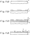
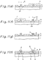
- Fig.1 shows the producing steps of a thin film transistor (TFT) on a glass substrate.
- TFT thin film transistor
- the embodiment is described for a CMOS-FET as an example of a TFT.
- a glass substrate must have the characteristics that it does not contract or reduce dimention at temperature 600°C.
- the size of glass does not reduce more than 5 ⁇ m/30 cm when glass is heated to 600 °C for long time.
- Neo-ceram glass (trade name) manufactured by Nippon Electric Glass Company. That glass has the following compositions.
- lead wires for external connection are provided through the conventional steps of providing thin holes on the insulation film 8, placing and patterning aluminium film.
- the lead wires for a gate electrode G, a source electrode S, and a drain electrode D are provided as shown in Fig.1(h) through the insulation film 8.
- CMOS-FET on a glass substrate through low temperature process is completed.
- One of the features of the present invention is the use of disilane gas for producing an amorphous silicon film which is subject to solid phase growth to change to non single crystal silicon film through heat treatment in nitrogen gas atmosphere.
- the characteristics of the amorphous silicon film with the parameter of gas (disilane gas or conventional silane gas), temperature, heat treatment condition, and film thickness are shown in the table 2, in which the samples 1 through 5 use disilane gas, and the sample 6 uses conventional silane gas.
- the samples 1 through 5 use disilane gas, and the producing conditions are;
- the sample 6 uses silane gas, and the producing conditions are that (20% SiH4/He) gas; 800 SCCM, and the pressure of 0.8 Torr.
- the samples 5 and 6 are out of the present invention, since the sample 5 has too thick film, and the sample 6 uses silane gas (not disilane gas).
- the oxygen density in the amorphous silicon film or the solid phase growth film is high as shown in the table 2.
- the oxygen density in the film 2′ must be less than 2x10¹⁹/cm3.
- the important factor for providing that low oxygen density is the growth rate of the film 2.
- the growth rate of the film 2 in the present invention is higher than 50 ⁇ /minute. The growth rate can be controlled by adjusting concentration of disilane gas, and flow rate of disilane gas.
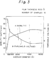
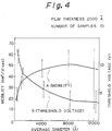
- Figs.2, 3 and 4 show characteristics curves of the mobility and the threshold voltage for each average diameter of a crystal grain in the solid phase growth film 2′.
- Fig.2 shows the case that the film thickness is 500 ⁇
- Fig.3 shows the case that the film thickness is 1000 ⁇
- Fig.4 shows the case that the film thickness is 2000 ⁇ .
- the number of samples in those figures is 10, and the case of P-channel is shown.
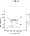
- Fig.5 shows the characteristics of the leak current A which is undesirable current when a transistor is in OFF state, and the threshold voltage B which is necessary gate voltage for switching a transistor, for each film thickness of the film 2′. As shown in Fig.5, when the film thickness is large, the leak currect A increases. As the leak current is preferable less than 1x10 ⁇ 8 (A) in a practical device, the film thickness must be less than 2000 ⁇ as far as the leak current concerns.
- Fig.5 shows the case of an N-channel transistor.
- the film thickness is preferably larger than 500 ⁇ in view of the mobility, and smaller than 2000 ⁇ in view of the leak current.
- the threshold voltage in those conditions of film thickness is less than 8 V as shown in the curve B of Fig.5.
- the film thickness is preferably in the range between 500 ⁇ and 2000 ⁇ , and the diameter of a crystal grain in the film 2′ is preferably in the range between 1/2 times and 4 times of the film thickness.
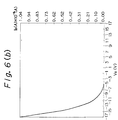
- Fig.6 shows the V G -I D (gate voltage - drain current) characteristics of the present MOS-FET produced on a non single crystal semiconductor film.
- Fig.6(a) shows the case of a N-channel transistor, and the mobility of 50 cm2/V ⁇ sec is obtained.
- Fig.6(b) shows the case of a P-channel transistor, and the mobility of 24 cm2/V ⁇ sec is obtained.
- Fig.7 shows a circuit diagram of a C-MOS inverter, and the operational waveforms of the same. It should be appreciated that the present C-MOS inverter operates with enough switching speed of 500 kHz, which is satisfactory operational speed for the use of an image sensor.
- the glass substrate in Fig.7 is LE30 (trade name) produced by Hoya Glass Company in Japan.
- the present invention which produces a thin film transistor in non single crystal semiconductor film which is produced on a glass substrate through low temperature process using di-silane gas, provides a thin film transistor with high mobility which is higher than 20 cm2/V ⁇ sec in P-channel, and higher than 50 cm2/V ⁇ sec in N-channel, and the threshold voltage is lower than 10 V.
- the present invention is applicable to a high speed switching device, an image sensor, and/or liquid crystal screen.
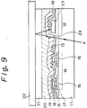
- the numeral 11 is a glass substrate
- 12 is a sensor section
- 13 is an opaque shadow film
- 14 is a thin film transistor section
- 15 is a non single crystal (solid phase growth) silicon section
- 16 is a gate electrode
- 17 is a gate oxide film
- 18 is a conductive (aluminium) electrode
- 19 is a protection film
- 20 is an adhesive
- 21 is a thin transparent plate
- 22 is a document which is subject to read
- 23 is a sensor element
- 24 is an illumination window.
- the image sensor of Fig.9 is a so-called contact type in which an image sensor and a document 22 contact directly.
- a light beam A illuminates the document 22 through the window 24, and the reflection beam reflected by the document 22 is read or converted to electrical signal by the sensor section 12.
- Each cell of the sensor section 12 comprises a sensor element 23, and a plurality of thin film transistors (TFT) which include a switching element for operating said sensor element.
- TFT thin film transistors
- Fig.10 shows a circuit diagram of an image sensor, which comprises a photo-diode Di, a switching transistor T ri for operating said photo-diode, and a flip-flop FFi for operating said switching transistor.
- the outputs of the photo-diodes are obtained at the signal output terminal through an amplifier AMP.
- the photo-diodes (photo sensor), and the related transistors (switching transistors and flip-flops) are produced on a non single crystal silicon film on a glass substrate according to the present invention.
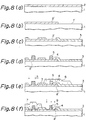
- Fig.8 shows the producing steps of the circuit of Fig.10, and only one photo sensor and a pair of transistors are shown for the sake of the simplicity.
- the glass substrate 1 with the amorphous silicon layer 2 is prepared as is the case of Fig.1(a) (see Fig.8(a)).
- the amorphous silicon film 2 is processed through solid phase growth to the solid phase growth film 2′ as is the case of Fig.1(b).
- the chemical conditions for solid phase growth is the same as that of Fig.1(b).
- the film 2′ is subject to photolithoetching process to provide an islant 2′ on which thin film transistors are provided (see Fig.8(b)).
- the right portion where no film 2′ exists is the section for depositing a photo sensor.
- a conductive film 9 made of chromium (Cr) is deposited on the film 8.
- the conductive film 9 functions both as a shadow film 13, and as one of electrodes of a photo-sensor.
- the SiO2 film 8 is provided with through holes through photolithoetching process, and then, a conductive film 12 which comprises a first chromium film with about 1000 ⁇ thickness and a second aluminium film of about 1 ⁇ m thickness is placed on the insulation film 8.
- the conductive film 12 is shaped to the wiring pattern for coupling each elements on the substrate through wet etching process (Fig.8(i)) so that a wire lead 12′ couples each elements (Fig.8(j)).
- a TFT portion on left half section in the drawing, and a photo sensor section on right half section in the drawing are completed.
Landscapes
- Engineering & Computer Science (AREA)
- Multimedia (AREA)
- Signal Processing (AREA)
- Thin Film Transistor (AREA)
Applications Claiming Priority (4)
| Application Number | Priority Date | Filing Date | Title |
|---|---|---|---|
| JP29412/91 | 1991-01-30 | ||
| JP02941191A JP3575698B2 (ja) | 1991-01-30 | 1991-01-30 | 多結晶半導体装置の製造方法 |
| JP3029412A JPH04245443A (ja) | 1991-01-30 | 1991-01-30 | 完全密着型イメ−ジセンサ |
| JP29411/91 | 1991-01-30 |
Publications (2)
| Publication Number | Publication Date |
|---|---|
| EP0497592A2 true EP0497592A2 (de) | 1992-08-05 |
| EP0497592A3 EP0497592A3 (en) | 1993-07-21 |
Family
ID=26367621
Family Applications (1)
| Application Number | Title | Priority Date | Filing Date |
|---|---|---|---|
| EP19920300787 Ceased EP0497592A3 (en) | 1991-01-30 | 1992-01-30 | Non single crystal semiconductor device and manufacturing method |
Country Status (2)
| Country | Link |
|---|---|
| US (2) | US5298455A (de) |
| EP (1) | EP0497592A3 (de) |
Cited By (7)
| Publication number | Priority date | Publication date | Assignee | Title |
|---|---|---|---|---|
| WO1995018463A1 (en) * | 1993-12-30 | 1995-07-06 | Honeywell Inc. | Single crystal silicon on quartz |
| EP0795202A4 (de) * | 1994-12-02 | 1998-06-24 | Pacific Solar Pty Ltd | Verfahren zur herstellung einer mehrschicht-solarzelle |
| CN100399125C (zh) * | 1993-06-12 | 2008-07-02 | 株式会社半导体能源研究所 | 具有薄膜晶体管的器件 |
| CN100452423C (zh) * | 1993-02-15 | 2009-01-14 | 株式会社半导体能源研究所 | 一种晶体管 |
| CN100521119C (zh) * | 1992-12-04 | 2009-07-29 | 株式会社半导体能源研究所 | 半导体器件及其制造方法 |
| US7622335B2 (en) | 1992-12-04 | 2009-11-24 | Semiconductor Energy Laboratory Co., Ltd. | Method for manufacturing a thin film transistor device |
| US8263926B2 (en) | 2005-05-23 | 2012-09-11 | Semiconductor Energy Laboratory Co., Ltd. | Photoelectric conversion device and manufacturing method thereof |
Families Citing this family (13)
| Publication number | Priority date | Publication date | Assignee | Title |
|---|---|---|---|---|
| US5576222A (en) * | 1992-01-27 | 1996-11-19 | Tdk Corp. | Method of making a semiconductor image sensor device |
| JPH0766424A (ja) * | 1993-08-20 | 1995-03-10 | Semiconductor Energy Lab Co Ltd | 半導体装置およびその作製方法 |
| JP3192546B2 (ja) * | 1994-04-15 | 2001-07-30 | シャープ株式会社 | 半導体装置およびその製造方法 |
| US6278127B1 (en) * | 1994-12-09 | 2001-08-21 | Agere Systems Guardian Corp. | Article comprising an organic thin film transistor adapted for biasing to form a N-type or a P-type transistor |
| US5625199A (en) * | 1996-01-16 | 1997-04-29 | Lucent Technologies Inc. | Article comprising complementary circuit with inorganic n-channel and organic p-channel thin film transistors |
| GB9603052D0 (en) * | 1996-02-14 | 1996-04-10 | Philips Electronics Nv | Image sensor |
| JPH11219133A (ja) * | 1998-02-02 | 1999-08-10 | Tdk Corp | 画像表示装置 |
| US6858898B1 (en) * | 1999-03-23 | 2005-02-22 | Semiconductor Energy Laboratory Co., Ltd. | Semiconductor device and method for manufacturing the same |
| US6461899B1 (en) | 1999-04-30 | 2002-10-08 | Semiconductor Energy Laboratory, Co., Ltd. | Oxynitride laminate “blocking layer” for thin film semiconductor devices |
| US8514165B2 (en) * | 2006-12-28 | 2013-08-20 | Semiconductor Energy Laboratory Co., Ltd. | Semiconductor device |
| EP1970951A3 (de) * | 2007-03-13 | 2009-05-06 | Semiconductor Energy Laboratory Co., Ltd. | Halbleiterbauelement und Herstellungsverfahren dafür |
| US8298887B2 (en) * | 2009-12-03 | 2012-10-30 | Applied Materials, Inc. | High mobility monolithic p-i-n diodes |
| US8836906B2 (en) * | 2010-04-23 | 2014-09-16 | Semiconductor Energy Laboratory Co., Ltd. | Display device with light receiving element under transparent spacer and manufacturing method therefor |
Family Cites Families (11)
| Publication number | Priority date | Publication date | Assignee | Title |
|---|---|---|---|---|
| US4176372A (en) * | 1974-03-30 | 1979-11-27 | Sony Corporation | Semiconductor device having oxygen doped polycrystalline passivation layer |
| JPS51128268A (en) * | 1975-04-30 | 1976-11-09 | Sony Corp | Semiconductor unit |
| US4363828A (en) * | 1979-12-12 | 1982-12-14 | International Business Machines Corp. | Method for depositing silicon films and related materials by a glow discharge in a disiland or higher order silane gas |
| US4727044A (en) * | 1984-05-18 | 1988-02-23 | Semiconductor Energy Laboratory Co., Ltd. | Method of making a thin film transistor with laser recrystallized source and drain |
| JPS6193663A (ja) * | 1984-10-12 | 1986-05-12 | Fujitsu Ltd | アモルフアスシリコントランジスタ |
| CA1239706A (en) * | 1984-11-26 | 1988-07-26 | Hisao Hayashi | Method of forming a thin semiconductor film |
| US4901133A (en) * | 1986-04-02 | 1990-02-13 | Texas Instruments Incorporated | Multilayer semi-insulating film for hermetic wafer passivation and method for making same |
| JPS6310573A (ja) * | 1986-07-02 | 1988-01-18 | Oki Electric Ind Co Ltd | 半導体装置の製造方法 |
| JP2560716B2 (ja) * | 1987-03-25 | 1996-12-04 | 株式会社日本自動車部品総合研究所 | 半導体素子及びその製造方法 |
| EP0585673B1 (de) * | 1987-10-09 | 1999-05-26 | Canon Kabushiki Kaisha | Bildlesegerät |
| EP0598409B1 (de) * | 1989-02-14 | 1998-11-18 | Seiko Epson Corporation | Verfahren zur Herstellung einer Halbleitervorrichtung |
-
1992
- 1992-01-27 US US07/825,552 patent/US5298455A/en not_active Expired - Lifetime
- 1992-01-30 EP EP19920300787 patent/EP0497592A3/en not_active Ceased
-
1994
- 1994-01-31 US US08/189,498 patent/US5442198A/en not_active Expired - Lifetime
Cited By (10)
| Publication number | Priority date | Publication date | Assignee | Title |
|---|---|---|---|---|
| CN100521119C (zh) * | 1992-12-04 | 2009-07-29 | 株式会社半导体能源研究所 | 半导体器件及其制造方法 |
| US7622335B2 (en) | 1992-12-04 | 2009-11-24 | Semiconductor Energy Laboratory Co., Ltd. | Method for manufacturing a thin film transistor device |
| US8062935B2 (en) | 1992-12-04 | 2011-11-22 | Semiconductor Energy Laboratory Co., Ltd. | Semiconductor device and method for manufacturing the same |
| US8278660B2 (en) | 1992-12-04 | 2012-10-02 | Semiconductor Energy Laboratory Co., Ltd. | Semiconductor device and method for manufacturing the same |
| CN100452423C (zh) * | 1993-02-15 | 2009-01-14 | 株式会社半导体能源研究所 | 一种晶体管 |
| CN100399125C (zh) * | 1993-06-12 | 2008-07-02 | 株式会社半导体能源研究所 | 具有薄膜晶体管的器件 |
| WO1995018463A1 (en) * | 1993-12-30 | 1995-07-06 | Honeywell Inc. | Single crystal silicon on quartz |
| EP0795202A4 (de) * | 1994-12-02 | 1998-06-24 | Pacific Solar Pty Ltd | Verfahren zur herstellung einer mehrschicht-solarzelle |
| US5942050A (en) * | 1994-12-02 | 1999-08-24 | Pacific Solar Pty Ltd. | Method of manufacturing a multilayer solar cell |
| US8263926B2 (en) | 2005-05-23 | 2012-09-11 | Semiconductor Energy Laboratory Co., Ltd. | Photoelectric conversion device and manufacturing method thereof |
Also Published As
| Publication number | Publication date |
|---|---|
| US5298455A (en) | 1994-03-29 |
| US5442198A (en) | 1995-08-15 |
| EP0497592A3 (en) | 1993-07-21 |
Similar Documents
| Publication | Publication Date | Title |
|---|---|---|
| EP0497592A2 (de) | Nicht-Einkristall-Halbleiteranordnung und Verfahren zur Herstellung | |
| US4624737A (en) | Process for producing thin-film transistor | |
| US6504175B1 (en) | Hybrid polycrystalline and amorphous silicon structures on a shared substrate | |
| US4351856A (en) | Semiconductor device and method of manufacturing the same | |
| US6087730A (en) | Electronic devices and their manufacture | |
| KR100621488B1 (ko) | 박막 트랜지스터와 이를 포함하는 전자 장치 | |
| WO1997015949A2 (en) | Electronic device manufacture | |
| KR100265871B1 (ko) | 반도체 장치와 그 제조방법 | |
| EP0082783A2 (de) | Verfahren zur Herstellung von Dünnschichttransistoren aus Silizium auf isolierendem Substrat | |
| US6043113A (en) | Method of forming self-aligned thin film transistor | |
| KR100662492B1 (ko) | 비정질막 결정화 방법 및 이를 적용한 액정표시소자의제조방법 | |
| JPH0758793B2 (ja) | 薄膜トランジスタの製造方法 | |
| JP2865284B2 (ja) | 薄膜半導体デバイス | |
| JP3029288B2 (ja) | 液晶表示装置 | |
| US5635707A (en) | Photoelectric conversion device for use in sensing light reflected from medium surface | |
| CA1305398C (en) | Method for producing high yield electrical contacts to n _amorphous silicon | |
| JP2603285B2 (ja) | 光導電型イメージセンサの製造方法 | |
| JP3175390B2 (ja) | 薄膜トランジスタ及びその製造方法 | |
| US20240234619A1 (en) | Method for manufacturing transparent thin film transistor-based photosensitive device | |
| JPH0556027B2 (de) | ||
| JP3229304B2 (ja) | 絶縁ゲート型電界効果トランジスタおよび半導体装置 | |
| JPH04245443A (ja) | 完全密着型イメ−ジセンサ | |
| Kołodziej et al. | Characteristics of hydrogenated amorphous silicon thin film transistors fabricated by dc magnetron sputtering | |
| JP2852919B2 (ja) | 液晶表示装置 | |
| JP3234201B2 (ja) | 半導体装置 |
Legal Events
| Date | Code | Title | Description |
|---|---|---|---|
| PUAI | Public reference made under article 153(3) epc to a published international application that has entered the european phase |
Free format text: ORIGINAL CODE: 0009012 |
|
| 17P | Request for examination filed |
Effective date: 19920221 |
|
| AK | Designated contracting states |
Kind code of ref document: A2 Designated state(s): DE FR GB |
|
| PUAL | Search report despatched |
Free format text: ORIGINAL CODE: 0009013 |
|
| AK | Designated contracting states |
Kind code of ref document: A3 Designated state(s): DE FR GB |
|
| 17Q | First examination report despatched |
Effective date: 19940204 |
|
| 18R | Application refused |
Effective date: 19980529 |