EP0497596B1 - Verfahren zum Herstellen von integrierten Schaltstrukturen - Google Patents
Verfahren zum Herstellen von integrierten Schaltstrukturen Download PDFInfo
- Publication number
- EP0497596B1 EP0497596B1 EP92300795A EP92300795A EP0497596B1 EP 0497596 B1 EP0497596 B1 EP 0497596B1 EP 92300795 A EP92300795 A EP 92300795A EP 92300795 A EP92300795 A EP 92300795A EP 0497596 B1 EP0497596 B1 EP 0497596B1
- Authority
- EP
- European Patent Office
- Prior art keywords
- conductive
- layer
- polycrystalline silicon
- substrate
- silicide
- Prior art date
- Legal status (The legal status is an assumption and is not a legal conclusion. Google has not performed a legal analysis and makes no representation as to the accuracy of the status listed.)
- Expired - Lifetime
Links
Images

Classifications
-
- H—ELECTRICITY
- H10—SEMICONDUCTOR DEVICES; ELECTRIC SOLID-STATE DEVICES NOT OTHERWISE PROVIDED FOR
- H10D—INORGANIC ELECTRIC SEMICONDUCTOR DEVICES
- H10D30/00—Field-effect transistors [FET]
- H10D30/01—Manufacture or treatment
- H10D30/021—Manufacture or treatment of FETs having insulated gates [IGFET]
- H10D30/0212—Manufacture or treatment of FETs having insulated gates [IGFET] using self-aligned silicidation
-
- H—ELECTRICITY
- H10—SEMICONDUCTOR DEVICES; ELECTRIC SOLID-STATE DEVICES NOT OTHERWISE PROVIDED FOR
- H10D—INORGANIC ELECTRIC SEMICONDUCTOR DEVICES
- H10D64/00—Electrodes of devices having potential barriers
- H10D64/01—Manufacture or treatment
- H10D64/011—Manufacture or treatment of electrodes ohmically coupled to a semiconductor
- H10D64/0111—Manufacture or treatment of electrodes ohmically coupled to a semiconductor to Group IV semiconductors
- H10D64/0112—Manufacture or treatment of electrodes ohmically coupled to a semiconductor to Group IV semiconductors using conductive layers comprising silicides
-
- H—ELECTRICITY
- H10—SEMICONDUCTOR DEVICES; ELECTRIC SOLID-STATE DEVICES NOT OTHERWISE PROVIDED FOR
- H10D—INORGANIC ELECTRIC SEMICONDUCTOR DEVICES
- H10D64/00—Electrodes of devices having potential barriers
- H10D64/01—Manufacture or treatment
- H10D64/013—Manufacture or treatment of electrodes having a conductor capacitively coupled to a semiconductor by an insulator
- H10D64/01302—Manufacture or treatment of electrodes having a conductor capacitively coupled to a semiconductor by an insulator the insulator being formed after the semiconductor body, the semiconductor being silicon
- H10D64/01304—Manufacture or treatment of electrodes having a conductor capacitively coupled to a semiconductor by an insulator the insulator being formed after the semiconductor body, the semiconductor being silicon characterised by the conductor
- H10D64/01306—Manufacture or treatment of electrodes having a conductor capacitively coupled to a semiconductor by an insulator the insulator being formed after the semiconductor body, the semiconductor being silicon characterised by the conductor the conductor comprising a layer of silicon contacting the insulator, e.g. polysilicon
- H10D64/01308—Manufacture or treatment of electrodes having a conductor capacitively coupled to a semiconductor by an insulator the insulator being formed after the semiconductor body, the semiconductor being silicon characterised by the conductor the conductor comprising a layer of silicon contacting the insulator, e.g. polysilicon the conductor further comprising a non-elemental silicon additional conductive layer, e.g. a metal silicide layer formed by the reaction of silicon with an implanted metal
- H10D64/0131—Manufacture or treatment of electrodes having a conductor capacitively coupled to a semiconductor by an insulator the insulator being formed after the semiconductor body, the semiconductor being silicon characterised by the conductor the conductor comprising a layer of silicon contacting the insulator, e.g. polysilicon the conductor further comprising a non-elemental silicon additional conductive layer, e.g. a metal silicide layer formed by the reaction of silicon with an implanted metal the additional conductive layer comprising a silicide layer formed by the silicidation reaction between the layer of silicon with a metal layer which is not formed by metal implantation
Definitions
- the present invention relates generally to semiconductor integrated circuit structures, and more specifically to a method for providing low resistance contact and interconnect structures.
- polycrystalline silicon interconnect layers and active areas in the substrate are used for providing electrical interconnections between devices formed within the substrate.
- Use of the active area for interconnect is necessary to achieve the high packing densities required for small geometry, high density circuits.
- SALICIDE Self-Aligned siliCIDE
- This process forms a conductivity enhancing refractory metal silicide layer in the selected active areas of the substrate simultaneously with silicidation of polycrystalline silicon gate and interconnect elements.
- the silicidation steps used to form these silicides are fairly straight forward and reliable, and are compatible with current standard process flows.
- IBM TECHNICAL DISCLOSURE BULLETIN (vol.22, no. 2, July 1979, pp. 598-599) discloses improving the conductivity of poly-Si gate structures using the transition metal silicide NbSi2.
- EP-A-0404372 discloses a semiconductor integrated circuit structure, and a method of manufacturing an integrated circuit, which comprises a first silicon layer, an insulating layer having a contact opening formed over said first silicon layer, a metal silicide layer covering said contact opening and a second polycrystalline silicon layer covering the metal silicide layer and at least a part of the insulating layer.
- the silicidation process does have some drawbacks.
- the process converts underlying silicon to a refractory metal silicide. If the polycrystalline silicon layer used to form the gate is too thin, so that the entire layer is converted to the refractory metal silicide, gate oxide integrities can be degraded. Additionally, the consumption of silicon in the substrate active areas can damage shallow junctions in the substrate. Increasing the thickness of the polycrystalline silicon layer used to form the gates will normally solve any problems relating to the silicidation of the gate and polycrystalline silicon interconnect. However, shallow junction depth is necessary for sub-micron integrated circuits, and the junctions cannot be deepened in most cases.
- the thickness of the silicide layer must be limited. This also limits the thickness of the silicide which can be formed on the polycrystalline silicon gate and interconnect elements. Since conductivity is improved for thicker silicides, it is normally desirable to provide the thickest possible silicide layer on the gate and interconnect layers which is consistent with gate integrity. However, only relatively thin silicides can be formed in the polycrystalline silicon to ensure that the active area junctions are protected.
- the present invention provides a method for forming a conductive interconnect structure for an integrated circuit formed in a silicon substrate having an active area with shallow junction regions therein, comprising the steps of:
- the present invention also provides a conductive interconnect structure consisting of a portion of a semiconductor integrated circuit comprising:
- an integrated circuit is to be formed in a semiconductor substrate 10 . Active areas will be defined between field oxide regions 12, 14 . Between the field oxide regions, a gate oxide layer 16 is grown over exposed portions of the substrate 10 . A layer of polycrystalline silicon 18 is then deposited over the surface of the device. A layer of tungsten silicide 20 is deposited over the polycrystalline silicon layer 18 . Tungsten silicide layer 20 is, as known in the art, highly conductive relative to polycrystalline silicon. Tungsten silicide layer 20 may be deposited, as known in the art, or it may be grown by depositing a tungsten layer over the polycrystalline silicon layer 18 , and heating the integrated circuit device to form the silicide layer 20 . If the latter approach is used, silicide formation is then followed by a wet etch to remove unreacted tungsten. A second polycrystalline silicon layer 22 is then formed over the silicide layer 20 .
- Both of the polycrystalline silicon layers 18, 22 are preferably doped to improve their conductivity.
- the level of doping need not be extremely high, inasmuch as the silicide layer 20 will be the primary current carrying structure.
- the polycrystalline silicon layers 18, 22 will likely make contact with other structures containing silicon, and doping the polycrystalline silicon layers 18, 22 can improve the quality of the contact with these other layers.
- Polycrystalline silicon layers 18, 22 may be initially formed with impurities, or may be doped after deposition by using, for example, ion implantation. If the process herein described is used in the formation of CMOS devices, it may be necessary to dope the polycrystalline silicon layers 18, 22 using ion implantation so that different portions of the layers 18, 22 can be doped P-type and N-type. This doping using different impurities may be necessary to prevent the formation of unwanted PN junctions where polycrystalline silicon layer 18 contacts N-type and P-type regions within the substrate 10 .
- the layers 18,20,22 are patterned and etched to define a gate electrode.
- Gate oxide 16 is typically used as an etch stop for the polycrystalline silicon layer 18, and is not removed at this time.
- Lightly doped drain regions 24 are then implanted by an implant 25 into the substrate 10 as known in the art.
- a layer of oxide (not shown) is deposited over the surface of the device, and antisotropically etched back to form sidewall regions 26. Formation of the sidewall oxide regions 26 generally removes any exposed portions of the oxide layer 16, resulting in the structure shown in Figure 3.
- a high impurity dosage implant 27 is then made to form source/drain regions 28 . These regions 28 fill the active_areas of the device which are not masked by the gate electrode and its sidewalls 26 . In addition to being used as source/drain regions suitable for later contacts, they are also used as current carrying interconnect structures between physically proximate transistors. After formation of the source/drain regions 28 , a layer 30 of refractory metal, preferably titanium, is formed over the surface of the device.
- the titanium layer 30 is then reacted in a nitrogen ambient, as known in the art, to form titanium silicide regions on the gate 32 , and in the active areas 34 .
- the thickness of the titanium layer 30 and the temperature and duration of the anneal period used to form the silicide are chosen so that the silicide regions 34 do not damage the integrity of the junctions underlying the source/drain regions 28 . Although this provides a thinner than normally desirable silicide region 32 on the gate electrode, the relatively thicker silicide region 20 lowers the overall resistivity of the gate electrode to desirable levels.
- any unreacted titanium and titanium nitride are then stripped from the device.
- An additional anneal step in a high temperature may be used, if desired, to provide more stable titanium silicide regions 32, 34, and improve the conductivity of these regions.
- the remainder of the fabrication process from this point is conventional, and may for example, include the formation of second and third level polycrystalline silicon layers, one or more layers of metal interconnect, and device passivation.
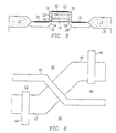
- Field oxide 40 surrounds an active region 42 .
- Gate electrode 44 overlies a portion of the active region 42 , with source/drain regions lying to either side thereof.
- gate electrode 46 overlies the active region 42 with source/drain regions lying to either side.
- the gate electrodes 44, 46 are preferably the same as that shown in Figure 4 ,having two different silicide layers and sidewall oxide spacers as shown in Figure 4 .
- a polycrystalline silicon interconnect lead 48 is formed from a second or third level polycrystalline silicon interconnect layer, and crosses over the active region 42 . Since conductive element 48 is formed at a later stage, active area 42 is continuous underneath it.
- the conductive element 48 is spaced above the active area 42 by at least one level of interlevel oxide, and the active area 42 is highly conductive due to its surface being silicided as described above, no field effect transistor is formed underneath the conductive element 48 where it crosses over the active area 42 .
- Active area 42 defines a conductive interconnect structure between the source/drain regions of the transistors defined by gate electrodes 44 and 46 . Since it is formed in the substrate, conductive element 48 can be formed in second level polysilicon. This allows the illustrated crisscross arrangement, such as might be found with the crosscoupled latches of an SRAM cell, to be easily fabricated.
- the preferred tungsten silicide conductive layer 20 may be replaced by any other conductive layer, such as another refractory silicide layer or a suitable refractory metal layer.
- the titanium silicide regions 32, 34 can be formed instead from other refractory metal silicides in the same manner.
- Another alternative step is to form the source/drain regions 28 after formation of the silicide regions 32 , 34 .
- the implantation of the source/drain regions 28 is simply delayed until after the SALICIDE step, and the source/drain regions 28 implanted through the silicide regions 34 .
- the method described above, and the structure formed thereby, provides a technique for performing a SALICIDE process with improved characteristics.
- a thinner silicide layer is formed over the active areas of the substrate in order to preserve the integrity of shallow junction regions.
- An extra conductive layer such as a tungsten silicide layer, is included in the gate and interconnect electrodes to ensure that their conductivity remains high.
- the preferred method is illustrated as being used with a first level polycrystalline silicon layer, it may also be used with polycrystalline silicon interconnect layer in which it is necessary or desirable to use to the SALICIDE process to form a silicide on the silicon layer simultaneously with one in the substrate, in which only a thin layer may be formed.
- the technique can be practiced when simultaneously siliciding a second or third layer polycrystalline silicon interconnect and the substrate. It can also be used when simultaneous silicidation must be performed of two or more different polycrystalline silicon interconnect layers, wherein at least one of such layers has only a thin layer of polycrystalline silicon and must not be silicided to a greater thickness.
Landscapes
- Electrodes Of Semiconductors (AREA)
- Internal Circuitry In Semiconductor Integrated Circuit Devices (AREA)
- Insulated Gate Type Field-Effect Transistor (AREA)
Claims (14)
- Verfahren zum Ausbilden einer leitenden Zwischenverbindungsstruktur für eine integrierte Schaltung, die in einem Siliziumsubstrat (10) ausgebildet ist, die einen aktiven Bereich (42) mit flachen Verbindungs- bzw. Verzweigungsbereichen darin aufweist, mit den folgenden Schritten:eine erste Schicht aus polykristallinem Silizium (18) wird zumindest über ausgewählten Bereichen der integrierten Schaltung ausgebildet, zu welchen eine Zwischenverbindung herzustellen ist;eine erste leitende Siliziumschicht (20) wird über der ersten polykristallinen Siliziumschicht (18) ausgebildet;eine zweite Schicht (22) aus polykristallinem Silizium wird über der ersten leitenden Siliziumschicht (20) ausgebildet;dadurch gekennzeichnet, daß das Verfahren ferner folgende Schritte aufweist:die erste und die zweite Schicht (18, 22) aus polykristallinem Silizium und die erste leitende Siliziumschicht (20) werden mit einem Muster versehen, um eine mehrschichtige leitende Struktur festzulegen;eine Schicht aus Metall (30) wird ausgebildet, die reagiert, um ein leitendes Silizid über der mehrschichtigen leitenden Struktur und freigelegten Bereichen des Substrats (10) auszubilden, die den aktiven Bereich (42) enthalten, der die darin festgelegten flachen Verbindungs- bzw. Anschlußbereiche aufweist; unddas Substrat (10), die zweite Schicht (22) aus polykristallinem Silizium und die Metallschicht (30) werden erhitzt, wobei die Erhitzung bei einer Temperatur durchgeführt wird, die ausreicht, um ein zweites leitendes Silizid (32, 34) zu erzeugen, das die erste leitende Silizidschicht (20) und das Substrat (10) bis zu einer flachen Tiefe überdeckt, ohne die flachen Verbindungs- bzw. Anschlußbereiche in dem aktiven Bereich (42) des Substrats (10) zu beeinträchtigen.
- Verfahren nach Anspruch 1, in dem der Schritt des Ausbildens einer Metallschicht (30), die reagiert, um ein leitendes Silizid auszubilden, aufweist, daß ein hochschmelzendes Metall bzw. schlecht entflammbares Metall über der Oberfläche der integrierten Schaltung abgeschieden wird, und ferner den Schritt aufweist, nicht durch eine Reaktion verarbeitetes hochschmelzendes bzw. schwer entflammbares Metall nach dem Erhitzungsschritt zu entfernen.
- Verfahren nach Anspruch 2, in dem das hochschmelzende bzw. schwer entflammbare Metall Titan aufweist und in dem die erste leitende Silizidschicht (20) Wolframsilizid aufweist.
- Verfahren nach Anspruch 1, das ferner folgenden Schritt aufweist:
vor dem Schritt zum Ausbilden der ersten Schicht aus polykristallinem Silizium wird eine Gateoxidschicht (16) über zumindest Abschnitten der integrierten Schaltung ausgebildet, wobei ein Abschnitt der mehrschichtigen leitenden Struktur ein Gate für eine Feldeffekteinrichtung zur Verfügung stellt. - Verfahren nach Anspruch 4, in dem der Schritt zum Ausbilden eines Musters Bereiche des Substrats (10) freilegt, die die Gateoxidschicht (16) unterlegen und ferner folgende Schritte aufweist:nach dem Schritt zur Ausbildung eines Musters werden Verunreinigungen bzw. Dotierungsstoffe (25) in das Substrat (10) implantiert, um leicht dotierte Drainbereiche (24) der Feldeffekteinrichtungen auszubilden; undSeitenwandoxidbereiche (26) werden entlang der Seiten bzw. Kanten vertikaler Seiten des Gates ausgebildet.
- Verfahren nach Anspruch 5, das ferner folgenden Schritt aufweist:
Verunreinigungen bzw. Dotierstoffe (27) werden in das Substrat (10) implantiert, um Source-/Drainbereiche (28) für die Feldeffekteinrichtung auszubilden, wobei die Implantierung nach dem Schritt zum Ausbilden der Seitenwandoxidbereiche (26) oder nach dem Erhitzungsschritt vorgesehen ist. - Verfahren nach Anspruch 1, in dem die ersten und zweiten leitenden Silizide (20, 32, 34) ein hochschmelzendes bzw. schwer entflammbares Metallsilizid aufweisen.
- Verfahren nach Anspruch 7, in dem die ersten und zweiten leitenden Silizide (20, 32, 34) leitende Metailsilizide sind, die verschiedene hochschmelzende bzw. schwer entflammbare Metalle enthalten.
- Leitende Zwischenverbindungs- bzw. Zwischenanschlußstruktur, die aus einem Abschnitt einer integrierten Halbleiterschaltung besteht, die aufweist:eine mehrschichtige leitende Struktur, die eine erste Schicht (18) aus polykristallinem Silizium, eine erste leitende Silizidschicht (20) auf der ersten polykristallinen Siliziumschicht (18) und eine zweite Schicht (22) aus polykristallinem Silizium auf der ersten leitenden Silizidschicht (20) aufweist;dadurch gekennzeichnet, daß die leitende Zwischenverbindungs- bzw. Zwischenanschlußstruktur ferner einen ersten leitenden Bereich enthält, der eine leitende Silizidschicht (34), die eine erste Dicke hat, darauf aufweist, wobei die mehrschichtige leitende Struktur eine zweite leitende Silizidschicht (32) auf der zweiten Schicht (22) aus polykristallinem Silizium hat, und die zweite leitende Silizidschicht (32) im wesentlichen die erste Dicke hat und von dem gleichen Material ausgebildet ist, wie die leitende Silizidschicht (34) auf dem ersten leitenden Bereich.
- Struktur nach Anspruch 9, in der die mehrschichtige leitende Struktur ein Gate für eine Feldeffekteinrichtung festlegt.
- Struktur nach Anspruch 10, die Seitenwandoxidabstandshalter (26) auf vertikalen Seiten des Gates aufweist.
- Struktur nach Anspruch 11, die ferner aufweist:einen zweiten leitenden Bereich, der eine leitende Silizidschicht (34) darauf aufweist, die eine erste Dicke hat;wobei die erste und die zweite leitende Schicht aktive Bereich in einem Substrat (10) festlegen und auf gegenüberliegenden Seiten des Gates zueinander beabstandet sind, um Source-/Drainbereiche zu definieren.
- Struktur nach Anspruch 9, in der der erste leitende Bereich in einem Substrat (10) liegt und einen leitenden Pfad zwischen zwei Feldeffekteinrichtungen festlegt.
- Struktur nach Anspruch 13, die ferner aufweist:
ein leitendes Zwischenverbindungs- bzw. Zwischenanschlußelement (48) aus polykristallinem Silizium, das den ersten leitenden Bereich (34) überkreuzt bzw. überquert und davon durch eine isolierende Schicht getrennt ist.
Applications Claiming Priority (2)
| Application Number | Priority Date | Filing Date | Title |
|---|---|---|---|
| US64865091A | 1991-01-31 | 1991-01-31 | |
| US648650 | 1991-01-31 |
Publications (3)
| Publication Number | Publication Date |
|---|---|
| EP0497596A2 EP0497596A2 (de) | 1992-08-05 |
| EP0497596A3 EP0497596A3 (en) | 1992-10-28 |
| EP0497596B1 true EP0497596B1 (de) | 1996-01-10 |
Family
ID=24601646
Family Applications (1)
| Application Number | Title | Priority Date | Filing Date |
|---|---|---|---|
| EP92300795A Expired - Lifetime EP0497596B1 (de) | 1991-01-31 | 1992-01-30 | Verfahren zum Herstellen von integrierten Schaltstrukturen |
Country Status (4)
| Country | Link |
|---|---|
| EP (1) | EP0497596B1 (de) |
| JP (1) | JPH0563189A (de) |
| KR (1) | KR920015622A (de) |
| DE (1) | DE69207442T2 (de) |
Families Citing this family (7)
| Publication number | Priority date | Publication date | Assignee | Title |
|---|---|---|---|---|
| KR950011983B1 (ko) * | 1992-11-23 | 1995-10-13 | 삼성전자주식회사 | 반도체 장치의 제조방법 |
| KR100250744B1 (ko) * | 1996-06-21 | 2000-05-01 | 김영환 | 반도체 소자의 폴리사이드층 형성 방법 |
| GB2319658B (en) * | 1996-09-21 | 2001-08-22 | United Microelectronics Corp | Method of fabricating a word line |
| TW316326B (en) * | 1996-09-21 | 1997-09-21 | United Microelectronics Corp | Manufacturing method of word line |
| KR100463597B1 (ko) * | 1997-09-29 | 2005-02-28 | 주식회사 하이닉스반도체 | 반도체소자의제조방법 |
| JPH11307765A (ja) * | 1998-04-20 | 1999-11-05 | Nec Corp | 半導体装置及びその製造方法 |
| US6630718B1 (en) * | 1999-07-26 | 2003-10-07 | Micron Technology, Inc. | Transistor gate and local interconnect |
Family Cites Families (3)
| Publication number | Priority date | Publication date | Assignee | Title |
|---|---|---|---|---|
| US4128670A (en) * | 1977-11-11 | 1978-12-05 | International Business Machines Corporation | Fabrication method for integrated circuits with polysilicon lines having low sheet resistance |
| US4389257A (en) * | 1981-07-30 | 1983-06-21 | International Business Machines Corporation | Fabrication method for high conductivity, void-free polysilicon-silicide integrated circuit electrodes |
| US4470189A (en) * | 1983-05-23 | 1984-09-11 | International Business Machines Corporation | Process for making polycide structures |
-
1992
- 1992-01-10 KR KR1019920000373A patent/KR920015622A/ko not_active Withdrawn
- 1992-01-30 JP JP4015474A patent/JPH0563189A/ja active Pending
- 1992-01-30 DE DE69207442T patent/DE69207442T2/de not_active Expired - Fee Related
- 1992-01-30 EP EP92300795A patent/EP0497596B1/de not_active Expired - Lifetime
Also Published As
| Publication number | Publication date |
|---|---|
| EP0497596A3 (en) | 1992-10-28 |
| DE69207442D1 (de) | 1996-02-22 |
| EP0497596A2 (de) | 1992-08-05 |
| DE69207442T2 (de) | 1996-06-27 |
| JPH0563189A (ja) | 1993-03-12 |
| KR920015622A (ko) | 1992-08-27 |
Similar Documents
| Publication | Publication Date | Title |
|---|---|---|
| US5480814A (en) | Process of making a polysilicon barrier layer in a self-aligned contact module | |
| US5757045A (en) | CMOS device structure with reduced risk of salicide bridging and reduced resistance via use of a ultra shallow, junction extension, ion implantation | |
| US6388296B1 (en) | CMOS self-aligned strapped interconnection | |
| US5744395A (en) | Low resistance, self-aligned, titanium silicide structures, using a single rapid thermal anneal procedure | |
| US6709950B2 (en) | Semiconductor device and method of manufacturing the same | |
| US6744104B1 (en) | Semiconductor integrated circuit including insulated gate field effect transistor and method of manufacturing the same | |
| US5798278A (en) | Method of forming raised source/drain regions in an integrated circuit | |
| US20080242013A1 (en) | Semiconductor device and a method of manufacturing the same | |
| EP0622844B1 (de) | Herstellungsverfahren von Kontakten mit niedrigem Widerstand an den Übergang zwischen Gebieten mit verschiedenen Leitungstypen | |
| US5918130A (en) | Transistor fabrication employing formation of silicide across source and drain regions prior to formation of the gate conductor | |
| EP0603360A1 (de) | Verfahren zur herstellung einer lokalen verbindung und eines hohen polisiliziumwiderstands | |
| US5891771A (en) | Recessed structure for shallow trench isolation and salicide process | |
| EP0404372B1 (de) | Verfahren zur Herstellung von polykristallinen Siliziumkontakten | |
| US6495408B1 (en) | Local interconnection process for preventing dopant cross diffusion in shared gate electrodes | |
| EP0497596B1 (de) | Verfahren zum Herstellen von integrierten Schaltstrukturen | |
| EP0526244B1 (de) | Verfahren zur Herstellung eines vergrabenen Kontaktes aus Polysilizium | |
| US5888875A (en) | Diffusion resistor structure with silicided contact areas, and methods of fabrication thereof | |
| US6162689A (en) | Multi-depth junction formation tailored to silicide formation | |
| US6284610B1 (en) | Method to reduce compressive stress in the silicon substrate during silicidation | |
| US6291890B1 (en) | Semiconductor device having a silicide structure | |
| KR100255134B1 (ko) | 반도체 장치 및 그 제조 방법 | |
| US6426533B2 (en) | Semiconductor device and manufacturing method thereof | |
| US5146309A (en) | Method for forming polycrystalline silicon contacts | |
| US6211000B1 (en) | Method of making high performance mosfets having high conductivity gate conductors | |
| KR19980014188A (ko) | 플럭 이온주입을 이용한 반도체장치 및 그 제조방법 |
Legal Events
| Date | Code | Title | Description |
|---|---|---|---|
| PUAI | Public reference made under article 153(3) epc to a published international application that has entered the european phase |
Free format text: ORIGINAL CODE: 0009012 |
|
| AK | Designated contracting states |
Kind code of ref document: A2 Designated state(s): DE FR GB IT |
|
| PUAL | Search report despatched |
Free format text: ORIGINAL CODE: 0009013 |
|
| AK | Designated contracting states |
Kind code of ref document: A3 Designated state(s): DE FR GB IT |
|
| 17P | Request for examination filed |
Effective date: 19930416 |
|
| 17Q | First examination report despatched |
Effective date: 19931116 |
|
| GRAA | (expected) grant |
Free format text: ORIGINAL CODE: 0009210 |
|
| AK | Designated contracting states |
Kind code of ref document: B1 Designated state(s): DE FR GB IT |
|
| ITF | It: translation for a ep patent filed | ||
| REF | Corresponds to: |
Ref document number: 69207442 Country of ref document: DE Date of ref document: 19960222 |
|
| ET | Fr: translation filed | ||
| PLBE | No opposition filed within time limit |
Free format text: ORIGINAL CODE: 0009261 |
|
| 26N | No opposition filed | ||
| PGFP | Annual fee paid to national office [announced via postgrant information from national office to epo] |
Ref country code: FR Payment date: 19980109 Year of fee payment: 7 |
|
| PGFP | Annual fee paid to national office [announced via postgrant information from national office to epo] |
Ref country code: GB Payment date: 19980121 Year of fee payment: 7 |
|
| PGFP | Annual fee paid to national office [announced via postgrant information from national office to epo] |
Ref country code: DE Payment date: 19980206 Year of fee payment: 7 |
|
| PG25 | Lapsed in a contracting state [announced via postgrant information from national office to epo] |
Ref country code: GB Free format text: LAPSE BECAUSE OF NON-PAYMENT OF DUE FEES Effective date: 19990130 |
|
| GBPC | Gb: european patent ceased through non-payment of renewal fee |
Effective date: 19990130 |
|
| PG25 | Lapsed in a contracting state [announced via postgrant information from national office to epo] |
Ref country code: FR Free format text: LAPSE BECAUSE OF NON-PAYMENT OF DUE FEES Effective date: 19990930 |
|
| PG25 | Lapsed in a contracting state [announced via postgrant information from national office to epo] |
Ref country code: DE Free format text: LAPSE BECAUSE OF NON-PAYMENT OF DUE FEES Effective date: 19991103 |
|
| REG | Reference to a national code |
Ref country code: FR Ref legal event code: ST |
|
| PG25 | Lapsed in a contracting state [announced via postgrant information from national office to epo] |
Ref country code: IT Free format text: LAPSE BECAUSE OF NON-PAYMENT OF DUE FEES Effective date: 20050130 |