EP0497644A1 - Lithografisches Verfahren für Halbleitersubstrat, insbesondere für die lokalisierte Behandlung eines hervorstehenden Teiles - Google Patents
Lithografisches Verfahren für Halbleitersubstrat, insbesondere für die lokalisierte Behandlung eines hervorstehenden Teiles Download PDFInfo
- Publication number
- EP0497644A1 EP0497644A1 EP92400105A EP92400105A EP0497644A1 EP 0497644 A1 EP0497644 A1 EP 0497644A1 EP 92400105 A EP92400105 A EP 92400105A EP 92400105 A EP92400105 A EP 92400105A EP 0497644 A1 EP0497644 A1 EP 0497644A1
- Authority
- EP
- European Patent Office
- Prior art keywords
- resin
- zone
- ablation
- creep
- window
- Prior art date
- Legal status (The legal status is an assumption and is not a legal conclusion. Google has not performed a legal analysis and makes no representation as to the accuracy of the status listed.)
- Granted
Links
Images

Classifications
-
- H—ELECTRICITY
- H10—SEMICONDUCTOR DEVICES; ELECTRIC SOLID-STATE DEVICES NOT OTHERWISE PROVIDED FOR
- H10P—GENERIC PROCESSES OR APPARATUS FOR THE MANUFACTURE OR TREATMENT OF DEVICES COVERED BY CLASS H10
- H10P76/00—Manufacture or treatment of masks on semiconductor bodies, e.g. by lithography or photolithography
- H10P76/20—Manufacture or treatment of masks on semiconductor bodies, e.g. by lithography or photolithography of masks comprising organic materials
- H10P76/204—Manufacture or treatment of masks on semiconductor bodies, e.g. by lithography or photolithography of masks comprising organic materials of organic photoresist masks
- H10P76/2041—Photolithographic processes
-
- G—PHYSICS
- G03—PHOTOGRAPHY; CINEMATOGRAPHY; ANALOGOUS TECHNIQUES USING WAVES OTHER THAN OPTICAL WAVES; ELECTROGRAPHY; HOLOGRAPHY
- G03F—PHOTOMECHANICAL PRODUCTION OF TEXTURED OR PATTERNED SURFACES, e.g. FOR PRINTING, FOR PROCESSING OF SEMICONDUCTOR DEVICES; MATERIALS THEREFOR; ORIGINALS THEREFOR; APPARATUS SPECIALLY ADAPTED THEREFOR
- G03F7/00—Photomechanical, e.g. photolithographic, production of textured or patterned surfaces, e.g. printing surfaces; Materials therefor, e.g. comprising photoresists; Apparatus specially adapted therefor
- G03F7/26—Processing photosensitive materials; Apparatus therefor
- G03F7/40—Treatment after imagewise removal, e.g. baking
-
- H—ELECTRICITY
- H10—SEMICONDUCTOR DEVICES; ELECTRIC SOLID-STATE DEVICES NOT OTHERWISE PROVIDED FOR
- H10P—GENERIC PROCESSES OR APPARATUS FOR THE MANUFACTURE OR TREATMENT OF DEVICES COVERED BY CLASS H10
- H10P95/00—Generic processes or apparatus for manufacture or treatments not covered by the other groups of this subclass
- H10P95/08—Planarisation of organic insulating materials
-
- Y—GENERAL TAGGING OF NEW TECHNOLOGICAL DEVELOPMENTS; GENERAL TAGGING OF CROSS-SECTIONAL TECHNOLOGIES SPANNING OVER SEVERAL SECTIONS OF THE IPC; TECHNICAL SUBJECTS COVERED BY FORMER USPC CROSS-REFERENCE ART COLLECTIONS [XRACs] AND DIGESTS
- Y10—TECHNICAL SUBJECTS COVERED BY FORMER USPC
- Y10S—TECHNICAL SUBJECTS COVERED BY FORMER USPC CROSS-REFERENCE ART COLLECTIONS [XRACs] AND DIGESTS
- Y10S438/00—Semiconductor device manufacturing: process
- Y10S438/94—Laser ablative material removal
-
- Y—GENERAL TAGGING OF NEW TECHNOLOGICAL DEVELOPMENTS; GENERAL TAGGING OF CROSS-SECTIONAL TECHNOLOGIES SPANNING OVER SEVERAL SECTIONS OF THE IPC; TECHNICAL SUBJECTS COVERED BY FORMER USPC CROSS-REFERENCE ART COLLECTIONS [XRACs] AND DIGESTS
- Y10—TECHNICAL SUBJECTS COVERED BY FORMER USPC
- Y10S—TECHNICAL SUBJECTS COVERED BY FORMER USPC CROSS-REFERENCE ART COLLECTIONS [XRACs] AND DIGESTS
- Y10S438/00—Semiconductor device manufacturing: process
- Y10S438/942—Masking
- Y10S438/948—Radiation resist
Definitions
- the present invention relates to the realization of a localized treatment such as, in particular, the formation of a window through a coating layer above a zone forming a projection on a substrate.
- said coating layer is a thin layer whose thickness is typically between 50 nm and 1000 nm, and when said substrate has a generally planar surface on which said zone has a height typically between 500 nm and 0.05 mm and a transverse dimension typically between 100 nm and 0.1 mm, approximately.
- the substrate consists of a semiconductor material
- the coating layer consists of a dielectric material and when a window has to be formed through this layer to allow contact to be made electric located on the substrate. This is particularly the case during the manufacture of certain semiconductor lasers to locate an electric current ensuring the injection of charge carriers in an active layer in the form of a ribbon which is internal to this laser.
- the present invention aims in particular to allow the formation of a window whose edges are more precisely aligned with those of a projection on which this window must be formed. And, for this purpose, it relates to a treatment process located on the surface, in particular lithography on a semiconductor substrate, process in which a protective resin is deposited outside a projecting area on which a treatment must be carried out, then a treatment means is applied to this resin and to this zone against which this resin constitutes protection, this process being characterized in that, before applying said treatment means, said protective resin is brought to moving by creep towards said projecting zone to at least increase its thickness in the immediate vicinity of this zone.
- Such displacement by creep makes it possible to constitute or reinforce a protective layer at the outer edge of the protruding zone by using for this purpose forces, such as surface tension or gravity forces, which are capable, in the absence of any spatially selective command, to limit their action at the edge of the protruding area, thanks to the profile of the sides of this area and possibly to a suitable choice of the wettability of the various areas of the substrate by the protective resin.
- forces such as surface tension or gravity forces
- FIG. 1 represents views along a transverse plane of a first substrate at successive stages of the implementation of a method according to the present invention.
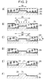
- FIG. 2 represents similar views of a second substrate at analogous stages of such a method.
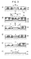
- FIG. 3 represents similar views of a third substrate at analogous stages of such a method.
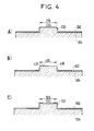
- FIG. 4 represents views of this second substrate, one after application of the method of the present invention and the others after application of lithography methods which are analogous but which do not use this invention.
- said anti-wetting condition is that the protective resin is non-wetting for said coating material.
- this same resin must have a certain adhesion to this same coating material during said resin deposition operation. This adhesion can in particular result from the fact that, during this deposition, this resin comprises a large proportion of a solvent which is volatile and which is then removed during annealing operations.
- This arrangement has the advantage that, to implement it, it suffices to choose a suitable resin. However, this requires that such a resin be available.
- an alternative arrangement would be, for example, that after the ablation of resin, one deposits on the coating layer, in the tray of the projecting area but not on the projecting sides, a product in a very thin layer which would oppose wetting by the resin.
- the effective width of the additional awareness strip may deviate from one theoretical width W1 which would be obtained in the absence of error. If we consider the maximum error that can affect this positioning, this effective width can be located randomly between a lower limit equal to the theoretical width minus the maximum error and an upper limit equal to the theoretical width plus the maximum error. We therefore choose a theoretical width greater than the maximum error. However, an excessively large theoretical width should not be chosen, which would require the resin to move by creep over a large distance, and would therefore unnecessarily oblige to create creep conditions which are relatively difficult to obtain.
- the width W2 of the awareness zone is advantageously chosen in the interval 2W0 ⁇ W2 ⁇ 3W0, W0 being the width of the protruding zone, which results in W0 / 2 ⁇ W1 ⁇ W0 (see Figure 2C).
- said spatially selective sensitization is exposure made by radiation 122 (FIG. 1B) through a removable mask 124.
- This arrangement has the advantage of using a photolithography process which is well known and which does not present of particular difficulty in the context of the present invention.
- a complete ablation of the resin is carried out by a second resin ablation process.
- said substrate is typically a semiconductor substrate and said coating layer is a dielectric layer.
- a conductive material is deposited to allow the passage of an electric current through the window formed. This deposit of conductive material is not shown.
- Figures 2 and 3 show elements homologous to those which have been mentioned with reference to Figure 1.
- their three reference numbers include the same tens and units digits, the hundreds digits being equal to the numbers of the corresponding figures.
- the substrate 104 is intended for the manufacture of a so-called buried ribbon semiconductor laser whose active layer 2 in the form of a ribbon extends perpendicular to the plane of the figure.
- This layer is framed by two isolation channels 4 and 6 which have been etched in this substrate over a limited width with a distance between axes D and a depth P. These channels leave between them the projecting area 106 whose width is close to 0.005 mm.
- Such lasers are known by the acronyms FBH or PBH, SIBC, DCPBH.
- W2 ⁇ D and H0 ⁇ P / 2 H0 being the thickness of resin deposited, during said resin deposition operation, on the unetched part of the substrate.
- the thickness of resin H1 removed during the gentle ablation operation of resin is then greater than H0 but less than H0 + P / 2.
- the formation of a projection results from an etching of the substrate 204 over the entire surface thereof except on the protruding area 206 whose width W0 is of the order of 0.002 mm.
- the method according to the present invention allows the localization of the injection of current into a laser crest known internationally as "laser ridge" and constituted by the projecting area 206 which extends perpendicular to the plane of the sheet (see FIG. 2C).
- H0 the thickness of resin deposited at a distance from the protruding area 206 and E the height of the plate of this area relative to the surrounding surface, it is advantageous for H0 to be at least equal to 2E.
- a projecting zone 306 results from the deposition of a filler material 8 on a substrate 304.
- This filler material was deposited in the form of a layer and then etched to form a ribbon which extends perpendicular to the plane of the figure and which has a width of the order of 0.001 mm.
- FIG. 4A corresponds to FIG. 2F, that is to say that it represents the result obtained by the method of the invention. It appears that the covering layer 202 remains, on the side such as 230 of the projecting zone 206, up to the vicinity of the plate 232 of this zone.
- the coating layer 402 is removed on the side 430 of the projecting area 406 to a relatively great distance from the plate 432 of this area.
- the coating layer 502 remains on the edges of the plate 532 of this zone.
- the coating layer 102 was made of silicon nitride and had a thickness H0 of 200 nm and the projecting zone 106 had a height P, for relative to the surrounding areas of the substrate 104, of the order of 2000 nm.
- the protective resin 208 a photosensitive resin of the genus novolaque sold under the reference TF20 and the trademark Microposit by the American firm Shipley. During the resin deposition operation, this resin was spread on a spinner at 5000 rpm for 30 seconds and then at 10,000 rpm for 3 seconds. Annealing at 90 ° C for 20 minutes was then carried out. The thickness obtained was 0.005 mm above the protruding area. The sunning operation lasted 25 seconds with a power of 20 mW / cm2. The ablation operation was done in two times fifteen seconds using a developer sold by the same company under the reference 351 and diluted in six volumes of water. It was checked with an optical microscope.
- the resin creep operation resulted from a annealing at a creep temperature of 150 ° C for 15 minutes.
- Window drilling through the dielectric coating (Si3N4) was done using a CF4 plasma (100 W, 15 minutes).
- the complete ablation of resin was done using a solvent sold by the American company General Chemical under the reference A20 Stripper.
- An important advantage of the method according to the present invention is that it dispenses with precise alignment of the exposure mask with respect to the projecting zones which it is desired to release.
- This process in fact provides "automatic" alignment (self-alignment) of the edges of the protective resin layer with those of the protruding zone during the creep operation.
- This self-alignment improves the quality of a component such as a semiconductor laser, the manufacture of which involves the implementation of this process.
- a second advantage is that a precise definition of the edge of the window does not require the support of a hard insolation mask on the surface of the substrate. It follows from the fact that the definition of the edge of the awareness zone can be relatively imprecise. It is important when working on fragile substrates such as those which consist of gallium arsenide GaAs or indium phosphorus InP.
Landscapes
- Physics & Mathematics (AREA)
- General Physics & Mathematics (AREA)
- Crystals, And After-Treatments Of Crystals (AREA)
- Drying Of Semiconductors (AREA)
- Semiconductor Lasers (AREA)
- Exposure And Positioning Against Photoresist Photosensitive Materials (AREA)
- Formation Of Insulating Films (AREA)
- Micromachines (AREA)
- Manufacture Or Reproduction Of Printing Formes (AREA)
- Encapsulation Of And Coatings For Semiconductor Or Solid State Devices (AREA)
Applications Claiming Priority (2)
| Application Number | Priority Date | Filing Date | Title |
|---|---|---|---|
| FR9100505A FR2671909B1 (fr) | 1991-01-17 | 1991-01-17 | Procede de lithogravure sur saillie notamment sur substrat semiconducteur. |
| FR9100505 | 1991-01-17 |
Publications (2)
| Publication Number | Publication Date |
|---|---|
| EP0497644A1 true EP0497644A1 (de) | 1992-08-05 |
| EP0497644B1 EP0497644B1 (de) | 1998-06-24 |
Family
ID=9408787
Family Applications (1)
| Application Number | Title | Priority Date | Filing Date |
|---|---|---|---|
| EP92400105A Expired - Lifetime EP0497644B1 (de) | 1991-01-17 | 1992-01-15 | Lithografisches Verfahren für Halbleitersubstrat, insbesondere für die lokalisierte Behandlung eines hervorstehenden Teiles |
Country Status (6)
| Country | Link |
|---|---|
| US (1) | US5283209A (de) |
| EP (1) | EP0497644B1 (de) |
| JP (1) | JPH04302489A (de) |
| DE (1) | DE69225985T2 (de) |
| ES (1) | ES2118119T3 (de) |
| FR (1) | FR2671909B1 (de) |
Cited By (1)
| Publication number | Priority date | Publication date | Assignee | Title |
|---|---|---|---|---|
| EP0614215A1 (de) * | 1993-03-05 | 1994-09-07 | Alcatel N.V. | Verfahren zur Herstellung eines Metallkontaktes auf einem Reliefmuster eines Halbleitersubstrates, mit einer Stufe zum plastischen Fliessen einer lichtempfindlichen Harzschicht |
Families Citing this family (1)
| Publication number | Priority date | Publication date | Assignee | Title |
|---|---|---|---|---|
| FR2695761B1 (fr) * | 1992-09-11 | 1994-12-30 | Slimane Loualiche | Procédé de fabrication de dispositifs électro-optiques à ruban, notamment de lasers, et dispositifs ainsi obtenus. |
Citations (2)
| Publication number | Priority date | Publication date | Assignee | Title |
|---|---|---|---|---|
| EP0300563A2 (de) * | 1987-07-20 | 1989-01-25 | Koninklijke Philips Electronics N.V. | Verfahren zur Herstellung von Halbleiterbauelementen wobei eine Oberfläche einer Halbleiterstruktur selektiv behandelt wird |
| WO1990001796A1 (de) * | 1988-08-04 | 1990-02-22 | Siemens Aktiengesellschaft | Verfahren zur einbettung und stufenabflachung von strukturierten oberflächen |
Family Cites Families (4)
| Publication number | Priority date | Publication date | Assignee | Title |
|---|---|---|---|---|
| US4722910A (en) * | 1986-05-27 | 1988-02-02 | Analog Devices, Inc. | Partially self-aligned metal contact process |
| JPS63104425A (ja) * | 1986-10-09 | 1988-05-09 | インタ−ナショナル・ビジネス・マシ−ンズ・コ−ポレ−ション | バイアの形成方法 |
| US5135891A (en) * | 1988-01-19 | 1992-08-04 | Mitsubishi Denki Kabushiki Kaisha | Method for forming film of uniform thickness on semiconductor substrate having concave portion |
| US5093225A (en) * | 1990-09-14 | 1992-03-03 | Gte Laboratories Incorporated | Processing method for fabricating electrical contacts to mesa structures in semiconductor devices |
-
1991
- 1991-01-17 FR FR9100505A patent/FR2671909B1/fr not_active Expired - Fee Related
-
1992
- 1992-01-15 EP EP92400105A patent/EP0497644B1/de not_active Expired - Lifetime
- 1992-01-15 ES ES92400105T patent/ES2118119T3/es not_active Expired - Lifetime
- 1992-01-15 DE DE69225985T patent/DE69225985T2/de not_active Expired - Fee Related
- 1992-01-17 US US07/824,259 patent/US5283209A/en not_active Expired - Fee Related
- 1992-01-17 JP JP4006854A patent/JPH04302489A/ja active Pending
Patent Citations (2)
| Publication number | Priority date | Publication date | Assignee | Title |
|---|---|---|---|---|
| EP0300563A2 (de) * | 1987-07-20 | 1989-01-25 | Koninklijke Philips Electronics N.V. | Verfahren zur Herstellung von Halbleiterbauelementen wobei eine Oberfläche einer Halbleiterstruktur selektiv behandelt wird |
| WO1990001796A1 (de) * | 1988-08-04 | 1990-02-22 | Siemens Aktiengesellschaft | Verfahren zur einbettung und stufenabflachung von strukturierten oberflächen |
Non-Patent Citations (2)
| Title |
|---|
| IBM TECHNICAL DISCLOSURE BULLETIN. vol. 32, no. 8B, Janvier 1990, NEW YORK US pages 443 - 445; ANONYME: 'Postsloped vias' * |
| MICROELECTRONIC ENGINEERING. vol. 9, no. 1-4, Mai 1989, AMSTERDAM NL pages 585 - 589; PANIEZ ET AL: 'Thermal flow properties of novolak polymers' * |
Cited By (2)
| Publication number | Priority date | Publication date | Assignee | Title |
|---|---|---|---|---|
| EP0614215A1 (de) * | 1993-03-05 | 1994-09-07 | Alcatel N.V. | Verfahren zur Herstellung eines Metallkontaktes auf einem Reliefmuster eines Halbleitersubstrates, mit einer Stufe zum plastischen Fliessen einer lichtempfindlichen Harzschicht |
| FR2702306A1 (fr) * | 1993-03-05 | 1994-09-09 | Alcatel Nv | Procédé d'auto-alignement d'un contact métallique sur un substrat de matériau semi-conducteur. |
Also Published As
| Publication number | Publication date |
|---|---|
| DE69225985T2 (de) | 1998-11-12 |
| EP0497644B1 (de) | 1998-06-24 |
| JPH04302489A (ja) | 1992-10-26 |
| FR2671909B1 (fr) | 1999-01-22 |
| ES2118119T3 (es) | 1998-09-16 |
| US5283209A (en) | 1994-02-01 |
| FR2671909A1 (fr) | 1992-07-24 |
| DE69225985D1 (de) | 1998-07-30 |
Similar Documents
| Publication | Publication Date | Title |
|---|---|---|
| EP0801419B1 (de) | Herstellungsverfahren von einem dünnen Halbleiterfilm, der elektronische Anordnungen enthält | |
| EP0660140B1 (de) | Herstellungsverfahren für eine Reliefstruktur auf einem Substrat aus Halbleitermaterial | |
| EP1114446B1 (de) | Herstellung einer dünnen membran | |
| FR3094573A1 (fr) | Procede de preparation d’une couche mince de materiau ferroelectrique | |
| FR2503457A1 (fr) | Systeme de cellules solaires connectees en serie sur un substrat unique | |
| CH678378A5 (de) | ||
| EP0221798A1 (de) | Verfahren zum Herstellen eines metallischen Verbindungsmusters für hochintegrierte Schaltungsbauelemente | |
| EP4309216A1 (de) | Verfahren zum übertragen einer schicht einer heterostruktur | |
| FR2969378A1 (fr) | Structure composite tridimensionnelle comportant plusieurs couches de microcomposants en alignement | |
| EP3948940A1 (de) | Verfahren zur übertragung von blöcken von einem donorsubstrat auf ein empfängersubstrat | |
| EP0199638A1 (de) | Verfahren zur Herstellung auf einem Isoliersubstrat eines gerichteten einkristallinen Siliziumfilms mit lokalisierten Fehlern | |
| EP0497644B1 (de) | Lithografisches Verfahren für Halbleitersubstrat, insbesondere für die lokalisierte Behandlung eines hervorstehenden Teiles | |
| EP0190243B1 (de) | Verfahren zur herstellung einer integrierten schaltung vom mis-typ | |
| FR2842647A1 (fr) | Procede de transfert de couche | |
| EP3678168B1 (de) | Ausheilverfahren vor dem transfer einer halbleiterschicht | |
| EP3453787A1 (de) | Herstellungsverfahren eines loses von mehrstufigen mikromechanischen metallteilen | |
| WO2004059386A1 (fr) | Procede de lithographie par pressage d'un substrat mettant en oeuvre une nano-impression | |
| EP0202977B1 (de) | Verfahren zur Herstellung auf einem Isoliersubstrat eines gerichteten einkristallinen Siliziumfilms mit lokalisierten Fehlern | |
| WO2024165363A1 (fr) | Structure integree comprenant une couche ferroelectrique a polarisation selective reportee sur un substrat et procede de fabrication | |
| EP3520132B1 (de) | Struktur mit einzelkristallhalbleiterinseln und verfahren zur herstellung solch einer struktur | |
| EP3503173A1 (de) | Übertragungsverfahren einer nutzschicht | |
| EP4060716A1 (de) | Verfahren zur veränderung eines spannungszustandes von mindestens einer halbleiterschicht | |
| FR3063834A1 (fr) | Procede de fabrication d'un dispositif semi-conducteur tridimensionnel | |
| EP4513269B1 (de) | Verfahren zur strukturierung eines substrats | |
| EP0550726B1 (de) | Verfahren zur herstellung einer ladungsübertragungsanordnung mit einem überlaufsystem |
Legal Events
| Date | Code | Title | Description |
|---|---|---|---|
| PUAI | Public reference made under article 153(3) epc to a published international application that has entered the european phase |
Free format text: ORIGINAL CODE: 0009012 |
|
| AK | Designated contracting states |
Kind code of ref document: A1 Designated state(s): DE ES FR GB IT NL SE |
|
| 17P | Request for examination filed |
Effective date: 19930108 |
|
| 17Q | First examination report despatched |
Effective date: 19941011 |
|
| GRAG | Despatch of communication of intention to grant |
Free format text: ORIGINAL CODE: EPIDOS AGRA |
|
| GRAG | Despatch of communication of intention to grant |
Free format text: ORIGINAL CODE: EPIDOS AGRA |
|
| GRAH | Despatch of communication of intention to grant a patent |
Free format text: ORIGINAL CODE: EPIDOS IGRA |
|
| GRAH | Despatch of communication of intention to grant a patent |
Free format text: ORIGINAL CODE: EPIDOS IGRA |
|
| GRAA | (expected) grant |
Free format text: ORIGINAL CODE: 0009210 |
|
| RAP1 | Party data changed (applicant data changed or rights of an application transferred) |
Owner name: ALCATEL ALSTHOM COMPAGNIE GENERALE D'ELECTRICITE |
|
| AK | Designated contracting states |
Kind code of ref document: B1 Designated state(s): DE ES FR GB IT NL SE |
|
| ITF | It: translation for a ep patent filed | ||
| REF | Corresponds to: |
Ref document number: 69225985 Country of ref document: DE Date of ref document: 19980730 |
|
| GBT | Gb: translation of ep patent filed (gb section 77(6)(a)/1977) |
Effective date: 19980723 |
|
| REG | Reference to a national code |
Ref country code: ES Ref legal event code: FG2A Ref document number: 2118119 Country of ref document: ES Kind code of ref document: T3 |
|
| RAP4 | Party data changed (patent owner data changed or rights of a patent transferred) |
Owner name: ALCATEL |
|
| RAP4 | Party data changed (patent owner data changed or rights of a patent transferred) |
Owner name: ALCATEL |
|
| PLBE | No opposition filed within time limit |
Free format text: ORIGINAL CODE: 0009261 |
|
| STAA | Information on the status of an ep patent application or granted ep patent |
Free format text: STATUS: NO OPPOSITION FILED WITHIN TIME LIMIT |
|
| 26N | No opposition filed | ||
| REG | Reference to a national code |
Ref country code: FR Ref legal event code: CD |
|
| PGFP | Annual fee paid to national office [announced via postgrant information from national office to epo] |
Ref country code: GB Payment date: 19991213 Year of fee payment: 9 |
|
| PGFP | Annual fee paid to national office [announced via postgrant information from national office to epo] |
Ref country code: NL Payment date: 19991216 Year of fee payment: 9 |
|
| PGFP | Annual fee paid to national office [announced via postgrant information from national office to epo] |
Ref country code: DE Payment date: 19991217 Year of fee payment: 9 |
|
| PGFP | Annual fee paid to national office [announced via postgrant information from national office to epo] |
Ref country code: SE Payment date: 19991220 Year of fee payment: 9 |
|
| PGFP | Annual fee paid to national office [announced via postgrant information from national office to epo] |
Ref country code: FR Payment date: 19991221 Year of fee payment: 9 |
|
| PGFP | Annual fee paid to national office [announced via postgrant information from national office to epo] |
Ref country code: ES Payment date: 20000121 Year of fee payment: 9 |
|
| PG25 | Lapsed in a contracting state [announced via postgrant information from national office to epo] |
Ref country code: GB Free format text: LAPSE BECAUSE OF NON-PAYMENT OF DUE FEES Effective date: 20010115 |
|
| PG25 | Lapsed in a contracting state [announced via postgrant information from national office to epo] |
Ref country code: SE Free format text: LAPSE BECAUSE OF NON-PAYMENT OF DUE FEES Effective date: 20010116 Ref country code: ES Free format text: LAPSE BECAUSE OF NON-PAYMENT OF DUE FEES Effective date: 20010116 |
|
| PG25 | Lapsed in a contracting state [announced via postgrant information from national office to epo] |
Ref country code: NL Free format text: LAPSE BECAUSE OF NON-PAYMENT OF DUE FEES Effective date: 20010801 |
|
| GBPC | Gb: european patent ceased through non-payment of renewal fee |
Effective date: 20010115 |
|
| EUG | Se: european patent has lapsed |
Ref document number: 92400105.0 |
|
| PG25 | Lapsed in a contracting state [announced via postgrant information from national office to epo] |
Ref country code: FR Free format text: LAPSE BECAUSE OF NON-PAYMENT OF DUE FEES Effective date: 20010928 |
|
| NLV4 | Nl: lapsed or anulled due to non-payment of the annual fee |
Effective date: 20010801 |
|
| PG25 | Lapsed in a contracting state [announced via postgrant information from national office to epo] |
Ref country code: DE Free format text: LAPSE BECAUSE OF NON-PAYMENT OF DUE FEES Effective date: 20011101 |
|
| REG | Reference to a national code |
Ref country code: FR Ref legal event code: ST |
|
| REG | Reference to a national code |
Ref country code: ES Ref legal event code: FD2A Effective date: 20020916 |
|
| PG25 | Lapsed in a contracting state [announced via postgrant information from national office to epo] |
Ref country code: IT Free format text: LAPSE BECAUSE OF NON-PAYMENT OF DUE FEES;WARNING: LAPSES OF ITALIAN PATENTS WITH EFFECTIVE DATE BEFORE 2007 MAY HAVE OCCURRED AT ANY TIME BEFORE 2007. THE CORRECT EFFECTIVE DATE MAY BE DIFFERENT FROM THE ONE RECORDED. Effective date: 20050115 |