EP0499100A2 - Procédé pour la fabrication des résistances confectionnées - Google Patents
Procédé pour la fabrication des résistances confectionnées Download PDFInfo
- Publication number
- EP0499100A2 EP0499100A2 EP92101601A EP92101601A EP0499100A2 EP 0499100 A2 EP0499100 A2 EP 0499100A2 EP 92101601 A EP92101601 A EP 92101601A EP 92101601 A EP92101601 A EP 92101601A EP 0499100 A2 EP0499100 A2 EP 0499100A2
- Authority
- EP
- European Patent Office
- Prior art keywords
- ptc element
- support
- ptc
- connecting wires
- cover
- Prior art date
- Legal status (The legal status is an assumption and is not a legal conclusion. Google has not performed a legal analysis and makes no representation as to the accuracy of the status listed.)
- Granted
Links
Images


Classifications
-
- H—ELECTRICITY
- H01—ELECTRIC ELEMENTS
- H01C—RESISTORS
- H01C17/00—Apparatus or processes specially adapted for manufacturing resistors
- H01C17/28—Apparatus or processes specially adapted for manufacturing resistors adapted for applying terminals
-
- H—ELECTRICITY
- H01—ELECTRIC ELEMENTS
- H01C—RESISTORS
- H01C1/00—Details
- H01C1/14—Terminals or tapping points specially adapted for resistors; Arrangements of terminals or tapping points on resistors
- H01C1/1406—Terminals or electrodes formed on resistive elements having positive temperature coefficient
-
- Y—GENERAL TAGGING OF NEW TECHNOLOGICAL DEVELOPMENTS; GENERAL TAGGING OF CROSS-SECTIONAL TECHNOLOGIES SPANNING OVER SEVERAL SECTIONS OF THE IPC; TECHNICAL SUBJECTS COVERED BY FORMER USPC CROSS-REFERENCE ART COLLECTIONS [XRACs] AND DIGESTS
- Y10—TECHNICAL SUBJECTS COVERED BY FORMER USPC
- Y10T—TECHNICAL SUBJECTS COVERED BY FORMER US CLASSIFICATION
- Y10T29/00—Metal working
- Y10T29/49—Method of mechanical manufacture
- Y10T29/49002—Electrical device making
- Y10T29/49082—Resistor making
- Y10T29/49085—Thermally variable
-
- Y—GENERAL TAGGING OF NEW TECHNOLOGICAL DEVELOPMENTS; GENERAL TAGGING OF CROSS-SECTIONAL TECHNOLOGIES SPANNING OVER SEVERAL SECTIONS OF THE IPC; TECHNICAL SUBJECTS COVERED BY FORMER USPC CROSS-REFERENCE ART COLLECTIONS [XRACs] AND DIGESTS
- Y10—TECHNICAL SUBJECTS COVERED BY FORMER USPC
- Y10T—TECHNICAL SUBJECTS COVERED BY FORMER US CLASSIFICATION
- Y10T29/00—Metal working
- Y10T29/49—Method of mechanical manufacture
- Y10T29/49002—Electrical device making
- Y10T29/49082—Resistor making
- Y10T29/49101—Applying terminal
Definitions
- the invention relates to a method for producing assembled self-stabilizing resistors, in particular for use on coil windings, such as for electric motors, two opposite side faces of a PTC element being electrically connected to connecting wires, and to a assembled self-stabilizing resistor, in particular for use on coil windings, such as for electric motors. with a flat PTC element and with this electrically connected connecting wires.
- Self-stabilizing resistors which have PTC elements, are used to monitor electrotechnical devices, in particular to monitor coil windings, such as those of electric motors or the like. with which electrical connection wires are connected.
- the resistors are partially wrapped in close thermal contact with the electrical device, such as the coil, for example by the coil winding wire.
- the connecting wires are soldered directly to the PTC elements, which are provided with a solderable metallic contact surface, such as a vapor-deposited silver coating.
- the connecting wires are usually soldered by hand.
- the invention is therefore based on the object of providing a method of the type mentioned at the outset which enables economical and inexpensive production of such assembled self-stabilizing resistors.
- the stated object is achieved by a method of the type mentioned at the outset, which is characterized in that support and cover surfaces for the PTC elements are punched out on a metallic carrier tape, that a PTC element is placed and fastened on each support surface in such a way that the cover surface is bent over the PTC element, the support and cover surfaces are provided with connecting wires, and the cover and support surfaces are separated from the rest of the carrier tape.
- a New assembled self-stabilizing resistor differs from the known resistors in that on opposite end faces of the PTC element sheet metal plates (support and cover surfaces) are soldered, which have superior approaches to the PTC element, to which the connecting wires are attached.
- the method according to the invention provides that the PTC elements, which form individual parts that are difficult to process by hand, are held and conveyed by a quasi-endless carrier tape during the assembly process - at least until the PTC elements are connected to connecting wires, which then can in turn be strapped in a manner known per se, whereupon the further automatic conveying can take place in a defined form and with a defined relative distance of the PTC elements through the straps engaging on the connecting wires.
- the PTC elements are kept defined and all machining and processing operations can be carried out fully automatically in the stations of a processing device.
- the PTC elements can be fed to the endless carrier belt from a vibrating pot either via a slide with a locking slide.
- the slide ends directly in front of the support surface for a PTC element on the carrier tape. If such a support surface was conveyed in front of the slide, the locking slide can release a PTC element so that it can slide onto the support surface. The others are then held back by the slide or corresponding slide.
- Positioning pins can be provided which center the PTC element on the contact surface.
- grippers can be provided which grip the PTC elements and place them on the support surface.
- a cover surface is brought over it, so that the PTC element is sandwiched between the support surface and the cover surface. If solder was previously applied to the support and cover surface, the PTC elements can now be soldered to the support and cover surface.
- PTC elements are also used here, which are provided with a metallic contact. The soldering can be done by high frequency. The PTC elements are then firmly connected to the carrier tape and are therefore conveyed through this to the further processing and processing stations.
- protruding approaches for fixing the connecting wires are punched out from the support and cover surface. This facilitates the attachment, preferably welding, of the connecting wires to the support and cover surface for producing electrical connection contacts to the PTC element.
- edges of the approaches are bent perpendicular to them.
- the cover surface comes to lie flat on the PTC element can be provided in advance that the top surface is first bent before it is bent over the PTC element from the plane of the carrier tape while maintaining its parallel extension to this.
- the offset of the top surface to the level of the carrier tape essentially corresponds to the thickness of the PTC element.
- the approaches to which the connecting wires are later attached show their usefulness, in particular if they are aligned parallel to one another, but are arranged offset from one another in plan view.
- contact pins can be pressed against the lugs in parallel from top to bottom. This makes it possible to guide the carrier tape through the temperature bath in a horizontal orientation. It is not necessary for a contact pin to pass through the bottom of the temperature bath tub from below is performed, which would require difficult sealing. Furthermore, it is also not necessary to connect the carrier tape in any way in order to bring it in a vertical direction, so that contact pins could run in a horizontal direction from both sides against the support and cover surface. Connecting the carrier tape or conveying it vertically, at least over partial areas, would also cause problems, among other things due to the inherent rigidity of the carrier tape.
- PTC elements identified as defective in the above checking step can then be removed from the carrier tape and thus eliminated by providing a punching device at an appropriate clock step distance from the testing device and the corresponding number of conveying cycles later the corresponding PTC element by punching the connecting tab from the carrier tape is eliminated.
- a single connecting wire can be attached to each of the approaches on the support and top surface.
- two or more PTC elements can also be connected in series.
- one end of a piece of wire is connected to the top surface of the first PTC element and the other end of the piece of wire is connected to the contact surface of the immediately following PTC element and that the contact surface of the first PTC element and the top surface of the second PTC element are each provided with individual wires or that for the series connection of three PTC elements in each case the first end of a connecting wire with the top surface of a preceding PTC element and the second end of the connecting wire in each case with the immediately following PTC element. element are connected and that the contact surface of the first PTC element and the top surface of the third PTC element are provided with individual connecting wires.
- the connecting wires are strapped after fastening.
- the ready-made resistors are conveyed for further processing, which may consist in that the PTC elements connected to the support and cover surface and provided with connecting wires are provided with an insulation layer, in particular in that the PTC elements connected to the support and cover surface Elements can be provided with a powder coating. Furthermore, a shrink sleeve can be pushed on and shrunk on.
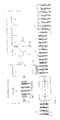
- the method according to the invention for producing self-stabilizing resistors for use on coil windings, such as for electric motors, is based on an endless carrier tape 1 made of thin sheet metal. Support surfaces 2 and cover surfaces 3 for PTC elements 4 are punched out of the carrier tape and are further held on a narrow holding strip 6 via connecting sections 7, 8 extending therefrom (method step A). On the cover and support surface 2, 3 extend essentially tangential lugs 9, 11 for later receiving and fixing connecting wires.
- Openings 12 are also punched out of the holding strip 6, by means of which, during further processing, an exact positioning of the holding strip 6 and thus also the cover and support surfaces 2, 3 can be effected.
- edges 13 (FIGS. 2a, b) of the projections 9, 11 are bent upwards in the plan view of FIG. 1.
- the top surface 3 is offset approximately as far from the plane of the carrier tape 6, but still lying parallel to it, as corresponds to the thickness of the PTC element 4.
- Cover and support surface 2, 3 can also be plate-shaped or bowl-shaped, as can be seen in FIG. 2b, so that edges 14 are formed which can encompass and center the PTC element 4 around its circumference.
- solder 16 is applied to the support and cover surface 2, 3.
- a PTC element in the form of a PTC pill is placed on the soldered support surface.
- the PTC elements can be conveyed on a vibrating pot 17 and either taken over by a gripper and placed on the support surface 2 or conveyed to the support surfaces 2 by means of a slide and an exposed stop.
- positioning pins 18 can be provided in addition to the contact surface 2, which, when a new contact surface 2 comes into their area, are moved upwards and hold the PTC element 4 between them.
- step E the tab 7 carrying the top surface 3 is bent in such a way that the top surface 3 is brought exactly over the PTC element 4. The result of this step is shown on the one hand in FIGS.
- the PTC element 4 and the support and cover surface 2, 3 are soldered to the previously applied solder 16.
- the soldering is preferably carried out at high frequency, that is to say by means of a high-frequency generator.
- the PTC element 4 has been fastened in this way to the support surface 2 and thus also the cover surface 3 has been fixed via the PTC element 4
- its carrier tab 7 can be separated from the carrier tape 6, for example at the point indicated by 19 (FIG. 2b). This takes place in method step G.
- the support surface 2 with the carrier tape 6 and the cover surface 3 are electrically separated from one another, so they no longer form a short-circuit connection.
- step J a cutting of defective PTC elements takes place, the faultiness being determined in the above-mentioned test process.
- the lugs 9, 11 are then provided with corresponding connecting wires 23, 24 (FIG. 3).
- a plurality of PTC elements 4 are to be interconnected in series, for example two PTC elements in a twin circuit or three PTC elements in a triplet circuit, as shown in FIG. 3, the connection ends 26, 27 of a U -shaped wire 23 connected on the one hand to the shoulder 11 of the cover part 3 of a PTC element (end 27) and on the other hand (end 26) to the shoulder 9 of the support part 2.
- the wire ends 26, 27 are preferably welded to the lugs 9, 11 (step K1). In step K1 'it can be seen how three successive PTC elements are connected in series with one another by two U-shaped connecting wires.
- step K2 the individual connecting strands 24 are attached to the free lugs 9 and 11, respectively.
- the connecting wires 23 are prepared in such a way that they are pulled off a wire roll, first of all at a front end in a stripping block 28 there is sufficient stripping of the front wire end, and then the wire is conveyed along two aligned grippers 29 that are pivotable relative to one another. After the required wire length has been reached, the piece of wire 23 is separated from the remaining wire and stripping is also carried out at the rear end (26).
- the grippers 29 pivot against one another and thereby bend the piece of wire 23 into the U-shape shown at the beginning of FIG. 3, in which the start (27) and end 26 of the wire reach the parallel orientation shown.
- connection wires 23, 24 After the connection wires 23, 24 have been attached, they are preferably taped, for example sandwiched between two adhesive tapes, which can be done in a conventional manner (step L). After the connecting wires 23, 24 and then the PTC elements are held by the belts 31, the PTC elements can be completely separated from the carrier tape 6 by a complete separation at 32 (FIG. 2b) (step M).
- the self-stabilizing resistors produced in this way can now be fed to further processing steps.
- Coating can be carried out, for example casting or powder coating.
- step N the initially horizontally conveyed resistors 33 are pivoted through 90 °, so that the connecting wires point upwards. This is done by passing the belt 31 between rollers 34, 36, which are provided in pairs and are perpendicular to one another.
- the resistors 33 are passed through a powder bath.
- the adhesion of the powders is then melted by heat that can be generated by a radiator 37, cools down again and forms a tight coating (step O).
- step O a shrink cap 3 can be pushed over the resistors 33.
- step P an endless hose 39
- step Q possibly closed in its free end and provided with a label
- It can be supported on a circular conveyor 39.
- step R the self-stabilizing Resistors 33 pushed on (step R), whereupon a shrinking process can finally follow in step S, so that the shrink cap 38 tightly envelops the resistor 33.
- step S the connecting wires 23, 24 can be shortened.
Landscapes
- Engineering & Computer Science (AREA)
- Microelectronics & Electronic Packaging (AREA)
- Manufacturing & Machinery (AREA)
- Apparatuses And Processes For Manufacturing Resistors (AREA)
- Thermistors And Varistors (AREA)
- Details Of Resistors (AREA)
- Non-Adjustable Resistors (AREA)
- Non-Insulated Conductors (AREA)
- Electronic Switches (AREA)
Priority Applications (1)
| Application Number | Priority Date | Filing Date | Title |
|---|---|---|---|
| EP95105563A EP0677855B1 (fr) | 1991-02-15 | 1992-01-31 | Résistance |
Applications Claiming Priority (2)
| Application Number | Priority Date | Filing Date | Title |
|---|---|---|---|
| DE4104709A DE4104709A1 (de) | 1991-02-15 | 1991-02-15 | Verfahren zum herstellen konfektionierter selbststabilisierender widerstaende und derartige widerstaende |
| DE4104709 | 1991-02-15 |
Related Child Applications (2)
| Application Number | Title | Priority Date | Filing Date |
|---|---|---|---|
| EP95105563.1 Division-Into | 1992-01-31 | ||
| EP95105563A Division EP0677855B1 (fr) | 1991-02-15 | 1992-01-31 | Résistance |
Publications (3)
| Publication Number | Publication Date |
|---|---|
| EP0499100A2 true EP0499100A2 (fr) | 1992-08-19 |
| EP0499100A3 EP0499100A3 (en) | 1993-04-21 |
| EP0499100B1 EP0499100B1 (fr) | 1996-05-08 |
Family
ID=6425140
Family Applications (2)
| Application Number | Title | Priority Date | Filing Date |
|---|---|---|---|
| EP92101601A Expired - Lifetime EP0499100B1 (fr) | 1991-02-15 | 1992-01-31 | Procédé pour la fabrication des résistances confectionnées |
| EP95105563A Expired - Lifetime EP0677855B1 (fr) | 1991-02-15 | 1992-01-31 | Résistance |
Family Applications After (1)
| Application Number | Title | Priority Date | Filing Date |
|---|---|---|---|
| EP95105563A Expired - Lifetime EP0677855B1 (fr) | 1991-02-15 | 1992-01-31 | Résistance |
Country Status (5)
| Country | Link |
|---|---|
| US (1) | US5239745A (fr) |
| EP (2) | EP0499100B1 (fr) |
| JP (1) | JP3270097B2 (fr) |
| AT (2) | ATE162332T1 (fr) |
| DE (3) | DE4104709A1 (fr) |
Cited By (1)
| Publication number | Priority date | Publication date | Assignee | Title |
|---|---|---|---|---|
| WO1998044516A1 (fr) * | 1997-03-27 | 1998-10-08 | Littelfuse, Inc. | Dispositif de protection de circuit automobile rearmable |
Families Citing this family (11)
| Publication number | Priority date | Publication date | Assignee | Title |
|---|---|---|---|---|
| JPH0831606A (ja) * | 1994-07-19 | 1996-02-02 | Murata Mfg Co Ltd | 電子部品 |
| DE29521353U1 (de) * | 1994-12-21 | 1997-02-06 | Renk Ag, 86159 Augsburg | Gleitlager |
| US5835004A (en) * | 1995-04-21 | 1998-11-10 | Raychem Corporation | Electrical devices and assemblies |
| GB9613216D0 (en) * | 1996-06-25 | 1996-08-28 | Bowthorpe Components Ltd | Thermistor device |
| US6058004A (en) * | 1997-09-08 | 2000-05-02 | Delaware Capital Formation, Inc. | Unitized discrete electronic component arrays |
| US6091317A (en) * | 1998-07-06 | 2000-07-18 | Ford Motor Company | Temperature sensor assembly |
| TW463184B (en) * | 1999-04-09 | 2001-11-11 | Murata Manufacturing Co | Temperature sensor, method of producing same and method of mounting same to a circuit board |
| US9587848B2 (en) | 2013-12-11 | 2017-03-07 | Honeywell International Inc. | Building automation controller with rear projecting light |
| US10488062B2 (en) | 2016-07-22 | 2019-11-26 | Ademco Inc. | Geofence plus schedule for a building controller |
| US10895883B2 (en) | 2016-08-26 | 2021-01-19 | Ademco Inc. | HVAC controller with a temperature sensor mounted on a flex circuit |
| CN119446694B (zh) * | 2024-12-10 | 2025-06-10 | 业展电子(惠州市)有限公司 | 合金电阻冲压装置、电阻生产工艺及合金电阻 |
Family Cites Families (10)
| Publication number | Priority date | Publication date | Assignee | Title |
|---|---|---|---|---|
| US3117297A (en) * | 1964-01-07 | figure | ||
| GB411512A (en) * | 1932-12-06 | 1934-06-06 | Pye Radio Ltd | Improvements in and relating to electric resistances |
| US2659871A (en) * | 1949-10-03 | 1953-11-17 | Aircraft Marine Prod Inc | Electrical connector strip having laterally displaced strip feeding edges |
| US3322655A (en) * | 1963-08-12 | 1967-05-30 | United Aircraft Corp | Method of making terminated microwafers |
| DE1490246B2 (de) * | 1964-06-23 | 1974-07-04 | Resista Fabrik Elektrischer Widerstaende Gmbh, 8300 Landshut | Verfahren zum Anbringen von Kontaktierangsteilen an elektrischen Bauelementen |
| DE2623606A1 (de) * | 1976-05-26 | 1977-12-08 | Draloric Electronic | Verfahren zur herstellung eines elektrischen schichtwiderstandes |
| JPH0690964B2 (ja) * | 1986-03-31 | 1994-11-14 | 日本メクトロン株式会社 | Ptc素子の製造法 |
| DE3703465C2 (de) * | 1987-02-05 | 1998-02-19 | Behr Thomson Dehnstoffregler | Verfahren zum Herstellen eines elektrischen Schaltgerätes und elektrisches Schaltgerät |
| US4926542A (en) * | 1988-08-26 | 1990-05-22 | Dale Electronic, Inc. | Method of making a surface mount wirewound resistor |
| JPH0311701A (ja) * | 1989-06-09 | 1991-01-21 | Murata Mfg Co Ltd | 正特性サーミスタ装置 |
-
1991
- 1991-02-15 DE DE4104709A patent/DE4104709A1/de not_active Withdrawn
-
1992
- 1992-01-31 AT AT95105563T patent/ATE162332T1/de not_active IP Right Cessation
- 1992-01-31 EP EP92101601A patent/EP0499100B1/fr not_active Expired - Lifetime
- 1992-01-31 AT AT92101601T patent/ATE137883T1/de not_active IP Right Cessation
- 1992-01-31 EP EP95105563A patent/EP0677855B1/fr not_active Expired - Lifetime
- 1992-01-31 DE DE59206205T patent/DE59206205D1/de not_active Expired - Fee Related
- 1992-01-31 DE DE59209141T patent/DE59209141D1/de not_active Expired - Fee Related
- 1992-02-14 JP JP02792192A patent/JP3270097B2/ja not_active Expired - Fee Related
- 1992-02-14 US US07/835,352 patent/US5239745A/en not_active Expired - Lifetime
Cited By (1)
| Publication number | Priority date | Publication date | Assignee | Title |
|---|---|---|---|---|
| WO1998044516A1 (fr) * | 1997-03-27 | 1998-10-08 | Littelfuse, Inc. | Dispositif de protection de circuit automobile rearmable |
Also Published As
| Publication number | Publication date |
|---|---|
| EP0499100A3 (en) | 1993-04-21 |
| DE59209141D1 (de) | 1998-02-19 |
| ATE137883T1 (de) | 1996-05-15 |
| DE59206205D1 (de) | 1996-06-13 |
| JP3270097B2 (ja) | 2002-04-02 |
| US5239745A (en) | 1993-08-31 |
| ATE162332T1 (de) | 1998-01-15 |
| EP0677855A1 (fr) | 1995-10-18 |
| JPH05226121A (ja) | 1993-09-03 |
| DE4104709A1 (de) | 1992-08-20 |
| EP0499100B1 (fr) | 1996-05-08 |
| EP0677855B1 (fr) | 1998-01-14 |
Similar Documents
| Publication | Publication Date | Title |
|---|---|---|
| EP0499100B1 (fr) | Procédé pour la fabrication des résistances confectionnées | |
| DE2444892C3 (de) | Verfahren zur Herstellung von streifenförmigen Anschlußelementen | |
| DE2315711A1 (de) | Verfahren zum kontaktieren von in einem halbleiterkoerper untergebrachten integrierten schaltungen mit hilfe eines ersten kontaktierungsrahmens | |
| DE4013391C2 (fr) | ||
| DE3304263A1 (de) | Glasschmelzsicherungen sowie verfahren zu ihrer herstellung | |
| DE69006114T2 (de) | Wicklungsträger und Verfahren zur Bildung eines Gefüges mit einer elektrischen Spule und einem elektronischen Bauteil mit Hilfe dieses Wicklungsträgers. | |
| DE69429899T2 (de) | Verfahren und Vorrichtung zum Aufwickelen eines Heizdrahtes | |
| DE69703720T2 (de) | Vorrichtung zur Herstellung von Kabelbäumen | |
| DE69401481T2 (de) | Flexibles Befestigungselement und Herstellungsverfahren | |
| DE2948319C2 (de) | Verfahren zum Anbringen und Befestigen von Stromzuführungsdrähten an elektrischen Bauelementen | |
| DE2346291A1 (de) | Verfahren und vorrichtung zum herstellen von leiterverbindungen und leiterendverbindungen durch aufbringen von verbindungsklemmen im schmelz-schweissverfahren | |
| EP0042137B1 (fr) | Procédé pour la fixation de fils d'interconnexion parallèles aux faces opposées de composants électriques | |
| WO2002031922A1 (fr) | Procede de connexion de cables plats | |
| DE69207622T2 (de) | Vorrichtung zur Herstellung von in leitender Folie gewickelten elektronischen Bauteilen | |
| DE2360360A1 (de) | Verbindungsklemme fuer isolierte leiter und verfahren zur herstellung einer solchen klemme | |
| DE2435399A1 (de) | Anschlussdraehte zum anloeten an flache schaltungstraeger | |
| DE3132965C2 (de) | Verfahren zum partiellen Abisolieren von isolierten Drähten | |
| DE2138083A1 (de) | Verfahren zum Anlöten von Ausgangsverbindungen an Kondensatoren und Nadel zur Herstellung der Ausgangsverbindungen | |
| DE60221723T2 (de) | Vorrichtung zur Zuführung von Verbindern und die damit ausgerüstete Krimpstation | |
| DE569830C (de) | Verfahren zur Herstellung von elektrischen Gluehdrahtzuendern | |
| DE2544770C2 (de) | Vorrichtung zum Anschlagen von Steckerstiften an elektrische Leitungen | |
| DE2527615A1 (de) | Verfahren und vorrichtung zur fixierung von kleinteilen | |
| DE2404825C3 (de) | Verfahren zur Herstellung von Bandleitungen kurzer Länge | |
| EP0081668B1 (fr) | Dispositif pour ceindre des composants électriques | |
| DE3308678A1 (de) | Verfahren zur herstellung elektromechanischer kontaktbauteile |
Legal Events
| Date | Code | Title | Description |
|---|---|---|---|
| PUAI | Public reference made under article 153(3) epc to a published international application that has entered the european phase |
Free format text: ORIGINAL CODE: 0009012 |
|
| AK | Designated contracting states |
Kind code of ref document: A2 Designated state(s): AT DE FR GB IT |
|
| PUAL | Search report despatched |
Free format text: ORIGINAL CODE: 0009013 |
|
| AK | Designated contracting states |
Kind code of ref document: A3 Designated state(s): AT DE FR GB IT |
|
| 17P | Request for examination filed |
Effective date: 19930403 |
|
| 17Q | First examination report despatched |
Effective date: 19941216 |
|
| RAP1 | Party data changed (applicant data changed or rights of an application transferred) |
Owner name: ERBENGEMEINSCHAFT PETER HOFSAESS: HOFSAESS, U. HOF |
|
| RIN1 | Information on inventor provided before grant (corrected) |
Inventor name: HOFSAESS, PETER |
|
| GRAH | Despatch of communication of intention to grant a patent |
Free format text: ORIGINAL CODE: EPIDOS IGRA |
|
| GRAA | (expected) grant |
Free format text: ORIGINAL CODE: 0009210 |
|
| AK | Designated contracting states |
Kind code of ref document: B1 Designated state(s): AT DE FR GB IT |
|
| REF | Corresponds to: |
Ref document number: 137883 Country of ref document: AT Date of ref document: 19960515 Kind code of ref document: T |
|
| XX | Miscellaneous (additional remarks) |
Free format text: TEILANMELDUNG 95105563.1 EINGEREICHT AM 28/07/95. |
|
| ITF | It: translation for a ep patent filed | ||
| REF | Corresponds to: |
Ref document number: 59206205 Country of ref document: DE Date of ref document: 19960613 |
|
| ET | Fr: translation filed | ||
| GBT | Gb: translation of ep patent filed (gb section 77(6)(a)/1977) |
Effective date: 19960725 |
|
| PLBE | No opposition filed within time limit |
Free format text: ORIGINAL CODE: 0009261 |
|
| STAA | Information on the status of an ep patent application or granted ep patent |
Free format text: STATUS: NO OPPOSITION FILED WITHIN TIME LIMIT |
|
| 26N | No opposition filed | ||
| REG | Reference to a national code |
Ref country code: GB Ref legal event code: IF02 |
|
| PGFP | Annual fee paid to national office [announced via postgrant information from national office to epo] |
Ref country code: GB Payment date: 20080124 Year of fee payment: 17 Ref country code: IT Payment date: 20080125 Year of fee payment: 17 |
|
| PGFP | Annual fee paid to national office [announced via postgrant information from national office to epo] |
Ref country code: AT Payment date: 20080116 Year of fee payment: 17 |
|
| PGFP | Annual fee paid to national office [announced via postgrant information from national office to epo] |
Ref country code: FR Payment date: 20080111 Year of fee payment: 17 |
|
| PGFP | Annual fee paid to national office [announced via postgrant information from national office to epo] |
Ref country code: DE Payment date: 20090224 Year of fee payment: 18 |
|
| GBPC | Gb: european patent ceased through non-payment of renewal fee |
Effective date: 20090131 |
|
| PG25 | Lapsed in a contracting state [announced via postgrant information from national office to epo] |
Ref country code: AT Free format text: LAPSE BECAUSE OF NON-PAYMENT OF DUE FEES Effective date: 20090131 |
|
| REG | Reference to a national code |
Ref country code: FR Ref legal event code: ST Effective date: 20091030 |
|
| PG25 | Lapsed in a contracting state [announced via postgrant information from national office to epo] |
Ref country code: GB Free format text: LAPSE BECAUSE OF NON-PAYMENT OF DUE FEES Effective date: 20090131 |
|
| PG25 | Lapsed in a contracting state [announced via postgrant information from national office to epo] |
Ref country code: FR Free format text: LAPSE BECAUSE OF NON-PAYMENT OF DUE FEES Effective date: 20090202 |
|
| PG25 | Lapsed in a contracting state [announced via postgrant information from national office to epo] |
Ref country code: DE Free format text: LAPSE BECAUSE OF NON-PAYMENT OF DUE FEES Effective date: 20100803 |
|
| PG25 | Lapsed in a contracting state [announced via postgrant information from national office to epo] |
Ref country code: IT Free format text: LAPSE BECAUSE OF NON-PAYMENT OF DUE FEES Effective date: 20090131 |