EP0499114A2 - Interne Getterung von Sauerstoff in III-V-Verbindungshalbleitern - Google Patents
Interne Getterung von Sauerstoff in III-V-Verbindungshalbleitern Download PDFInfo
- Publication number
- EP0499114A2 EP0499114A2 EP92101763A EP92101763A EP0499114A2 EP 0499114 A2 EP0499114 A2 EP 0499114A2 EP 92101763 A EP92101763 A EP 92101763A EP 92101763 A EP92101763 A EP 92101763A EP 0499114 A2 EP0499114 A2 EP 0499114A2
- Authority
- EP
- European Patent Office
- Prior art keywords
- iii
- reactive element
- oxygen
- dopant
- oxygen reactive
- Prior art date
- Legal status (The legal status is an assumption and is not a legal conclusion. Google has not performed a legal analysis and makes no representation as to the accuracy of the status listed.)
- Withdrawn
Links
Images


Classifications
-
- H—ELECTRICITY
- H10—SEMICONDUCTOR DEVICES; ELECTRIC SOLID-STATE DEVICES NOT OTHERWISE PROVIDED FOR
- H10P—GENERIC PROCESSES OR APPARATUS FOR THE MANUFACTURE OR TREATMENT OF DEVICES COVERED BY CLASS H10
- H10P30/00—Ion implantation into wafers, substrates or parts of devices
- H10P30/20—Ion implantation into wafers, substrates or parts of devices into semiconductor materials, e.g. for doping
- H10P30/202—Ion implantation into wafers, substrates or parts of devices into semiconductor materials, e.g. for doping characterised by the semiconductor materials
- H10P30/206—Ion implantation into wafers, substrates or parts of devices into semiconductor materials, e.g. for doping characterised by the semiconductor materials into Group III-V semiconductors
-
- H—ELECTRICITY
- H10—SEMICONDUCTOR DEVICES; ELECTRIC SOLID-STATE DEVICES NOT OTHERWISE PROVIDED FOR
- H10P—GENERIC PROCESSES OR APPARATUS FOR THE MANUFACTURE OR TREATMENT OF DEVICES COVERED BY CLASS H10
- H10P30/00—Ion implantation into wafers, substrates or parts of devices
- H10P30/20—Ion implantation into wafers, substrates or parts of devices into semiconductor materials, e.g. for doping
- H10P30/208—Ion implantation into wafers, substrates or parts of devices into semiconductor materials, e.g. for doping of electrically inactive species
-
- H—ELECTRICITY
- H10—SEMICONDUCTOR DEVICES; ELECTRIC SOLID-STATE DEVICES NOT OTHERWISE PROVIDED FOR
- H10P—GENERIC PROCESSES OR APPARATUS FOR THE MANUFACTURE OR TREATMENT OF DEVICES COVERED BY CLASS H10
- H10P30/00—Ion implantation into wafers, substrates or parts of devices
- H10P30/20—Ion implantation into wafers, substrates or parts of devices into semiconductor materials, e.g. for doping
- H10P30/21—Ion implantation into wafers, substrates or parts of devices into semiconductor materials, e.g. for doping of electrically active species
-
- H—ELECTRICITY
- H10—SEMICONDUCTOR DEVICES; ELECTRIC SOLID-STATE DEVICES NOT OTHERWISE PROVIDED FOR
- H10P—GENERIC PROCESSES OR APPARATUS FOR THE MANUFACTURE OR TREATMENT OF DEVICES COVERED BY CLASS H10
- H10P30/00—Ion implantation into wafers, substrates or parts of devices
- H10P30/20—Ion implantation into wafers, substrates or parts of devices into semiconductor materials, e.g. for doping
- H10P30/28—Ion implantation into wafers, substrates or parts of devices into semiconductor materials, e.g. for doping characterised by an annealing step, e.g. for activation of dopants
-
- H—ELECTRICITY
- H10—SEMICONDUCTOR DEVICES; ELECTRIC SOLID-STATE DEVICES NOT OTHERWISE PROVIDED FOR
- H10P—GENERIC PROCESSES OR APPARATUS FOR THE MANUFACTURE OR TREATMENT OF DEVICES COVERED BY CLASS H10
- H10P95/00—Generic processes or apparatus for manufacture or treatments not covered by the other groups of this subclass
- H10P95/40—Treatments of semiconductor bodies to modify their internal properties, e.g. to produce internal imperfections
- H10P95/408—Treatments of semiconductor bodies to modify their internal properties, e.g. to produce internal imperfections of Group III-V semiconductors, e.g. to render them semi-insulating
-
- Y—GENERAL TAGGING OF NEW TECHNOLOGICAL DEVELOPMENTS; GENERAL TAGGING OF CROSS-SECTIONAL TECHNOLOGIES SPANNING OVER SEVERAL SECTIONS OF THE IPC; TECHNICAL SUBJECTS COVERED BY FORMER USPC CROSS-REFERENCE ART COLLECTIONS [XRACs] AND DIGESTS
- Y10—TECHNICAL SUBJECTS COVERED BY FORMER USPC
- Y10S—TECHNICAL SUBJECTS COVERED BY FORMER USPC CROSS-REFERENCE ART COLLECTIONS [XRACs] AND DIGESTS
- Y10S148/00—Metal treatment
- Y10S148/024—Defect control-gettering and annealing
Definitions
- the technical field to which this invention relates is a method of placing an n-dopant in a III-V compound with an added oxygen reactive element to form a semiconductor with improved activation and electron mobility.
- the invention also relates to gettering oxygen from a III-V compound, especially a III-V compound semiconductor by means of an added oxygen reactive element to obtain this improvement.
- U.S. Patent 3,974,002 describes the use of aluminum as a gettering agent in MBE fabrication of heterostructure junction lasers based on GaAs compounds.
- Figure 3B of Casey illustrates alternating regions of GaAs and Al 0.25 Ga 0.75 As, i.e. a structure in which the aluminum gettering agent is employed in doses of about 25%.
- U.S. Patent 4,426,237 describes a method for growing GaAs by molecular beam epitaxy wherein Al is added to the Ga source crucible in order to improve Mg doping efficiency. No more than about 0.1% Al is included in the Ga source material e.g. 10 ⁇ 3 mole Al/mole GaAs.
- the patentees note that aluminum contamination of the GaAs region that is formed does not present a problem since the aluminum is used in such small amounts.
- Castl et a l. in IBM Technical Disclosure Bulletin Vol. 12, No. 11 April 1970 describe a method for gettering fast diffusing impurities from semiconductor materials by depositing aluminum on the back of a silicon wafer after the opposite side is processed to form an integrated circuit or similar device.
- the resultant structure is heat treated at a temperature of about 600°C for about one-half hour and during heat treatment the fast diffusing impurities within the silicon, such as copper, are removed by the gettering action of the aluminum film.
- Poponiak et al ., IBM Technical Disclosure Bulletin, Vol. 16, No. 4 September 1973 describe a gettering technique by which a damaged region or region is created in a semiconductor body for gettering purposes without materially disturbing the device regions.
- Nonconductive impurities such as Ge and Sn are ion implanted into a monocrystalline semiconductor body at an energy sufficient to cause penetration to a distance significantly below the surface.
- a damaged region or region is formed thereby, and afterwards the semiconductor is heated at a temperature and for a time sufficient to anneal the defects above the damaged region.
- Impurities are gettered in a silicon semiconductor wafer of a given conductivity type having an oxide region, such as a doped silicon oxide region disposed on a first or front surface of the wafer.
- a damaged region is formed by implanting ions into the wafer through the second or back surface of the wafer to a depth no closer to the first surface than the deepest depletion region of devices such as field-effect transistors, to be later formed in the first surface.
- Ions which may be implanted include B +, P+, Ar+, O+, Xe+, Si+, N+ or As+.
- the present invention as claimed provides a method for manufacturing a III-V semiconductor material MESFET having improved electrical activation and mobility of electrons in the channel region and an article of manufacture obtained thereby, the III-V semiconductor material being preferably a III-V semiconductor material based on GaAs.
- the present invention further obtains the foregoing advantages with a III-V semiconductor material that has been doped with an n-type material, the n-type material being preferably silicon.
- the present invention comprises a method for improving both the electrical activation and mobility of electrons in semiconductor materials such as III-V materials and the article of manufacture obtained thereby. It has been found that when n-type dopants are introduced into a III-V semiconductor crystal having minor amounts of oxygen as an impurity, and an oxygen reactive element co-implanted in a region opposite the dopant region, that both the electrical activation and mobility of the electrons in the semiconductor device thus produced improves markedly and in some instances by more than 20% compared to a control sample where a III-V crystal was implanted with an n-dopant without a co-implanted oxygen reactive element.
- the implanted oxygen reactive element acts as a gettering agent for the oxygen, to form an oxygen depleted zone between the n-dopant region and the implanted oxygen reactive element region.
- the implanted element employed in this respect will be referred to as an implanted oxygen reactive element and comprises any element that may be implanted or otherwise added to the III-V crystal or its equivalents, and will have an affinity for, or chemical reactivity with oxygen that is greater than the affinity or chemical reactivity of the III-V constituent atoms with oxygen or the dopant with oxygen.
- the implanted oxygen reactive element will be chosen so that it is more competitive than the III-V constituent atoms or dopant in the reaction with oxygen, i.e.
- the oxygen will selectively react with the implanted oxygen reactive element exclusively or to a greater degree than with the III-V constituent atoms with oxygen or the dopant with oxygen. Additionally, the implanted oxygen reactive element and the concentration employed, is selected so that it will not interfere with the electrical properties of the substrate (but in fact improve them) and must also be compatible with the process or processes used for forming the article of manufacture made according to the invention.
- the present invention also relates to a method of gettering oxygen from such a III-V compound by placing a dopant in the compound to form a dopant region and an oxygen reactive element to form an opposed region so that the implanted oxygen reactive element acts as a gettering agent to combine with the oxygen to form an oxygen depleted zone between the regions.
- the depth of, and space between the regions is sufficient so that oxygen combined with the implanted oxygen reactive element will not substantially interfere with the electrical properties of the dopant.
- the dopant and implanted oxygen reactive element are in a sufficiently low dose so that they will improve the electrical properties of the III-V semiconductor thus obtained, the implanted oxygen reactive element, in one embodiment being at a lower dose than the dopant.
- the dopant region, implanted oxygen reactive element region and oxygen depleted zone are formed so that the oxygen depleted zone also extends from the surface of the dopant region that is opposite the implanted oxygen reactive element region.
- the dopant region and the implanted oxygen reactive element region may be ion implanted into the III-V compound.
- a novel III-V semiconductor article of manufacture is also obtained containing minor amounts of oxygen, a dopant region and an opposed implanted oxygen element region with an oxygen depleted zone between the regions where the regions are spaced and the doses of dopant and implanted oxygen reactive element are as noted above.
- Metal - semiconductor - field - effect - transistors may be constructed from III-V materials such as gallium arsenide doped with an n-type material such as silicon to produce a source and a drain region straddling a channel operatively associated with a gate electrode.
- Source and drain electrodes are similarly associated with the source and drain regions.
- the flow of current between the source and the drain electrodes is controlled by the channel and the gate electrode associated with it, which operates in a manner analogous to a switch.
- the speed with which the device can be switched on and off by the appropriate application of current to the gate electrode depends on the amount of electrical charge and the mobility of the carriers [electrons in the case of n-dopants] in the channel region.
- the MESFET speed of operation can be increased which has significant commercial applications.
- higher speed switching allows for the faster processing of data which is to say an increased output of the computer.
- the method and article of manufacture of the present invention which comprises substantially increasing the electrical activation and mobility of the electrons in a III-V semiconductor material by doping a III-V crystalline material with an n-type dopant and adding or implanting an oxygen reactive element in the III-V material where the doses of dopant and implanted oxygen reactive element are low enough to improve the electrical activation and mobility of the electrons in the III-V semiconductor, especially where these doses do not exceed about 1E13 cm ⁇ 2.
- the added or implanted oxygen reactive element is at a dose substantially less than the n-type dopant and especially at a dose of from about 0.75 to about 0.2 times the dose of the n-type dopant.
- III-V semiconductor material may be employed although GaAs and InAs materials are preferred, especially GaAs materials and similarly any added or implanted oxygen reactive element may be used according to the invention but especially Al.
- both the electrical activation and mobility of the electrons improved markedly (more than 20%) compared to a control sample where Si was implanted without Al.
- the speed of a MESFET device is dependent to a great degree on the channel region of the device and the electric charge and mobility in this channel region.
- This channel region is semiconductive and in III-V devices typically comprises a Si doped region.
- the electric charge and the mobility in the channel region thus produced is improved in that the charge can be oscillated at a greater rate, the rate of this oscillation being correlated to the speed with which the device can be switched.
- the present invention in the channel region of a MESFET device higher speed switching can be obtained which, as noted before, has significant commercial application in computer devices in that the data processing speed and capacity of the device is thereby increased.
- the added or implanted oxygen reactive element that is used according to the invention acts as a gettering agent in semiconductor grades III-V crystalline materials such as GaAs which contains minor amounts of oxygen as an impurity.
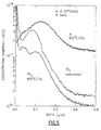
- III-V crystals such as GaAs are implanted with 18O and an oxygen reactive element such as Al, that a zone is produced in the GaAs crystal during annealing subsequent to implantation that has a reduced oxygen content i.e. an oxygen depleted zone results.
- Additional data, also reported herein indicate that the oxygen depleted zone created by the oxygen movement toward the aluminum where the alumunium concentration is the highest.
- the inventors do not wish to be limited by any theory, it appears that the electrical activation and mobility of the electrons is improved according to the invention where the n-type dopant is introduced into the III-V crystal to form a dopant region and the implanted oxygen reactive element similarly introduced into the III-V compound to form an implanted oxygen reactive region separate from and opposed to the dopant region.
- the implanted oxygen reactive element is introduced through the surface of the III-V compound to form a region beneath the surface.
- the dopant may then be introduced into the surface above the peak of the implanted oxygen reactive element region.
- the zone between the two regions is substantially oxygen depleted.
- this oxygen depleted zone also extends from the surface of the dopant region that is opposite the implanted oxygen reactive element region towards and optionally contiguous with the surface of the III-V compound. It is also within the scope of the invention to reverse the order of placement of the dopant and implanted oxygen reactive element or to add or implant them simultaneously.
- the implanted oxygen reactive element region is greater than or approximately twice the depth of the dopant layer.
- the dopant region may be implanted in the device anywhere from about 30 nm to about 500 nm (300 ⁇ to about 5,000 ⁇ ) and especially from about 20 nm to about 100 nm (200 ⁇ to about 1,000 ⁇ ) beneath the surface of the III-V compound.
- the oxygen depleted zone extending from the surface of the dopant layer opposite the gettering layer may be anywhere from about 0 nm to about 500 nm (0 ⁇ to about 5,000 ⁇ ), and especially from about 0nm to about 300 nm (0 ⁇ to about 3,000 ⁇ ).
- the invention is not to be limited to the separation of the two dosage peaks of the dopant and implanted oxygen reaction element, since some preliminary data also suggest that these two peaks can overlap or abut one another and some comparable electrical activation and mobility of the electrons in the channel obtained, provided that the oxygen reactive element such as Al is kept low i.e. within the ranges set forth herein. In the preferred embodiment of the invention, however, the regions of peak dose of each are maintained at a distance from one another, especially the range of distances specified herein.
- the preferred method of forming the implanted oxygen reactive element region and the dopant region is by ion implantation employing conventional operating conditions and apparatus for this process.
- the depth of the implanted regions are dependent on the energy which the ions of the implanted oxygen reactive element or dopant are injected into the III-V compound. The higher the voltage of the ion implantation apparatus (which can be adjusted), the deeper the implant of the implanted oxygen reactive element or dopant.
- the III-V compound is annealed in order to repair any damage to the crystalline structure of the III-V compound that results from the ion implantation process. It is believed that the oxygen in the III-V compound is mobile such as shown in Fig. 5 during annealing and will be brought into contact with and react with the implanted oxygen reactive element during this process.
- the annealing may be conducted preferably in one step or after each region is formed (whether implanted oxygen reactive element region or dopant region). In any event, annealing temperatures greater than about 600°C are utilized over a period of time from about 2 to about 60 seconds and especially a temperature from about 600°C to about 1000°C for a period of time from about 2 to about 10 seconds is employed.
- III-V compounds that may be treated according to the method of the invention are those based on Group IIIA of the Periodic Table of the Elements and Group VA from the Periodic Table of the Elements such as GaAs, InAs, GaP or InP and their art known equivalents.
- the various dopants that may be employed comprise, Si, Ge, Sn, Se and Te and at a range of doses from about 1E12 cm ⁇ 2 to about ⁇ 2E13 cm ⁇ 2 and especially from about 4E12 cm ⁇ 2 to about ⁇ 1E13 cm ⁇ 2.
- the implanted oxygen reactive element suitable for practicing the method of the present invention include B, Mg, Al, Be, Ti, Cr, Fe and Mn.
- the implanted oxygen reactive element dose should be less than about 1E13 cm ⁇ 2 and especially from less than about 4.5E12 cm ⁇ 2 to about 1.5E12 cm ⁇ 2.
- implanted oxygen reactive elements are especially effective according to the present invention where the concentration of oxygen in the III-V compound is from about 1E15 cm ⁇ 3 to about 1E17 cm ⁇ 3 and especially from about 1E15 cm ⁇ 3 to about 1E16 cm ⁇ 3, i.e. minor amounts of oxygen.
- the invention is especially useful in the preparation of III-V semiconductor materials having oxygen concentrations at a level of about ⁇ 1E17 cm ⁇ 3 as is found in semiconductor grades of GaAs.
- aluminum dosages slightly less than 1E13 cm ⁇ 2 are ion implanted at 160keV and up to a depth of about 0.2-0.3 micrometers in a GaAs substrate followed by implantation of Si at a voltage of less than 50 keV form an oxygen reactive element region and a dopant region in the GaAs compound.
- the implanted substrate is then subjected to a rapid thermal anneal without a cap at 900°C or below for a period of time from about 10 to about 60 seconds.
- the dopant region such as Si may be at the surface of the III-V compound or from about 50 nm to about 200 nm (500 ⁇ to about 2,000 ⁇ ) from the implanted oxygen reactive element region so that an oxygen depleted zone also extends from the surface of said dopant opposite the implanted oxygen reactive element region.
- Carrier concentrations-depth profile data measured by the C-V method were obtained by implanting Si and Si with Al in a GaAs crystal by ion beam implantation followed by capless RTA, the experimental conditions and results being reported by way of Fig. 1 which demonstrates that an addition of Al at 160 keV to a dose of 4.5E12 cm ⁇ 2 show a marked improvement in peak carrier concentration.
- the peak dose improves from about 4E17 cm ⁇ 3 for Si alone to about 5.5.E17 cm ⁇ 3 for the co-implantation of Si with Al. This is significant in that with Si in combination with Al, lower doses of Si are sufficient to achieve the same threshold voltage as with higher Si doses without Al.
- the lowering of the Si dose yields higher mobility in the channel region i.e. the gate and with the higher mobility, a higher speed device is obtained.
- Silicon and Al were co-implanted in a GaAs crystal by ion beam implantation and the Si and Al atomic concentration along with the relative depth distributions determined employing the SIMS method, the results of which are reported in Fig. 2 which also sets forth the ion implantation conditions, concentrations and RTA conditions.
- the peak concentration of the Al implant is at about 0.2 ⁇ m whereas the peak concentration of the Si is at about 0.05 ⁇ m.
- concentrations are obtained by employing different ion beam voltages for the Si and Al implants and consequently the so-called regions of Si dopant can be maintained at one level of peak concentration and the regions of Al dopant region obtained at a different concentration, but the regions are separate from one another which is to say that the regions of peak concentration of n-dopant such as Si and the region of peak concentration of the implanted oxygen reactive element are opposite one another and spaced by a measurable difference.
- the region of peak concentration of the Si dopant is spaced about 0.15 ⁇ m from the region of peak concentration of the implanted Al even though there is some overlap between the two.
- the maximum carrier concentration is obtained at a depth of about 0.05 ⁇ m which is not the maximum concentration of implanted Al which is at about 0.2 ⁇ m.
- Example 2 The method of Example 2 was repeated at different Al doses to determine the concentration limit of the Al co-implants.
- the carrier concentration increases with Al doses of 1.5E12 cm ⁇ 2 and 4.5E12 cm ⁇ 2 at 160 keV but then deteriorates at higher Al doses i.e. at 1E13 cm ⁇ 2.
- the experimental conditions and results are set forth in Fig. 3 where all curves are for Si co-implanted with Al. This is in agreement with the Farley, et al . ( supra ) data where the Al doses are higher than 1E13 cm ⁇ 2.
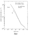
- Example 2 The method of Example 2 was repeated using Se as a n-dopant the experimental conditions employed and the results being set forth in Fig. 4.
- the increase in carrier concentration is improved by about one order of magnitude by the co-implantation of Al (4.5E12 cm ⁇ 2) with Se (7E12 cm ⁇ 2) as compared to Se alone.
- Additional data indicate that when the GaAs crystal is implanted with Si by ion implantation at 30 keV and a dose of 7.9E12 cm ⁇ 2 and co-implantation of Al at 160 keV at doses ranging from 1.5E12 cm ⁇ 2, 4.5E12 cm ⁇ 2, 1.0E13 cm ⁇ 2 and 5.0E13 cm ⁇ 2 that the sheet resistance increases unacceptably at the two highest Al doses. Accordingly the upper limit of the implanted oxygen reactive element appears to be about 4.5E12 cm ⁇ 2 at these n-dopant levels.
- regions under the source and drain electrode can be doped with Si in doses of about 4.5E13 cm ⁇ 2 whereas the channel region (i.e. the gate region) in between the source and drain regions can be doped with Si at lower doses e.g. about 4-7E12 cm ⁇ 2.
- a blanket Al implant over the gate region can be effected within the limits of the present invention to obtain increased electrical activation and mobility of the electrons in the channel without disturbing the electrical activation and mobility of the source region and the drain region.
Landscapes
- Junction Field-Effect Transistors (AREA)
Applications Claiming Priority (2)
| Application Number | Priority Date | Filing Date | Title |
|---|---|---|---|
| US07/655,512 US5183767A (en) | 1991-02-14 | 1991-02-14 | Method for internal gettering of oxygen in iii-v compound semiconductors |
| US655512 | 1996-05-30 |
Publications (2)
| Publication Number | Publication Date |
|---|---|
| EP0499114A2 true EP0499114A2 (de) | 1992-08-19 |
| EP0499114A3 EP0499114A3 (en) | 1992-12-09 |
Family
ID=24629192
Family Applications (1)
| Application Number | Title | Priority Date | Filing Date |
|---|---|---|---|
| EP19920101763 Withdrawn EP0499114A3 (en) | 1991-02-14 | 1992-02-04 | Internal gettering of oxygen in iii-v compound semiconductors |
Country Status (3)
| Country | Link |
|---|---|
| US (1) | US5183767A (de) |
| EP (1) | EP0499114A3 (de) |
| JP (1) | JPH05226343A (de) |
Families Citing this family (6)
| Publication number | Priority date | Publication date | Assignee | Title |
|---|---|---|---|---|
| JP2666757B2 (ja) * | 1995-01-09 | 1997-10-22 | 日本電気株式会社 | Soi基板の製造方法 |
| US5653801A (en) * | 1995-04-06 | 1997-08-05 | University Of Maryland Baltimore County | Method for reducing contamination in semiconductor by selenium doping |
| US5773356A (en) * | 1996-02-20 | 1998-06-30 | Micron Technology, Inc. | Gettering regions and methods of forming gettering regions within a semiconductor wafer |
| US5831513A (en) * | 1997-02-04 | 1998-11-03 | United Microelectronics Corp. | Magnetic field sensing device |
| US6146973A (en) * | 1997-12-12 | 2000-11-14 | Advanced Micro Devices, Inc. | High density isolation using an implant as a polish stop |
| US6335562B1 (en) | 1999-12-09 | 2002-01-01 | The United States Of America As Represented By The Secretary Of The Navy | Method and design for the suppression of single event upset failures in digital circuits made from GaAs and related compounds |
Family Cites Families (10)
| Publication number | Priority date | Publication date | Assignee | Title |
|---|---|---|---|---|
| DE2004849B2 (de) * | 1970-02-03 | 1975-06-05 | Siemens Ag, 1000 Berlin Und 8000 Muenchen | Verfahren zum Herstellen eines mit Silicium oder Germanium dotierten Galliumarsenidkristalls durch Kristallisation |
| DE2021345A1 (de) * | 1970-04-30 | 1972-01-13 | Siemens Ag | Verfahren zum Herstellen von sauerstoffarmen Galliumarsenid unter Verwendung von Silicium oder Germanium als Dotierstoff |
| US3647389A (en) * | 1970-05-11 | 1972-03-07 | Bell Telephone Labor Inc | Method of group iii-v semiconductor crystal growth using getter dried boric oxide encapsulant |
| US3974002A (en) * | 1974-06-10 | 1976-08-10 | Bell Telephone Laboratories, Incorporated | MBE growth: gettering contaminants and fabricating heterostructure junction lasers |
| JPS56155531A (en) * | 1980-04-30 | 1981-12-01 | Fujitsu Ltd | Manufacture of semiconductor device |
| US4383869A (en) * | 1981-06-15 | 1983-05-17 | Rca Corporation | Method for enhancing electron mobility in GaAs |
| US4426237A (en) * | 1981-10-13 | 1984-01-17 | International Business Machines Corporation | Volatile metal oxide suppression in molecular beam epitaxy systems |
| US4602965A (en) * | 1984-03-13 | 1986-07-29 | Communications Satellite Corporation | Method of making FETs in GaAs by dual species implantation of silicon and boron |
| JPS60235799A (ja) * | 1984-05-08 | 1985-11-22 | Nec Corp | 半絶縁性GaAs結晶の成長方法 |
| JPS61256675A (ja) * | 1985-05-09 | 1986-11-14 | Sumitomo Electric Ind Ltd | シヨツトキゲ−ト電界効果トランジスタの製造方法 |
-
1991
- 1991-02-14 US US07/655,512 patent/US5183767A/en not_active Expired - Fee Related
-
1992
- 1992-02-04 EP EP19920101763 patent/EP0499114A3/en not_active Withdrawn
- 1992-02-13 JP JP4026427A patent/JPH05226343A/ja active Pending
Also Published As
| Publication number | Publication date |
|---|---|
| EP0499114A3 (en) | 1992-12-09 |
| JPH05226343A (ja) | 1993-09-03 |
| US5183767A (en) | 1993-02-02 |
Similar Documents
| Publication | Publication Date | Title |
|---|---|---|
| US5318915A (en) | Method for forming a p-n junction in silicon carbide | |
| US9159783B2 (en) | Semiconductor device and substrate with chalcogen doped region | |
| US6992355B2 (en) | Semiconductor-on-insulator constructions | |
| EP0269349A2 (de) | Verfahren zur Herstellung eines Bauelementes mit einer tiefen Schicht aus Si02 | |
| Garcia et al. | High-quality CMOS in thin (100 nm) silicon on sapphire | |
| US4602965A (en) | Method of making FETs in GaAs by dual species implantation of silicon and boron | |
| JPH0677473A (ja) | ダイヤモンド電界効果トランジスタ及びその製造方法 | |
| US4816893A (en) | Low leakage CMOS/insulator substrate devices and method of forming the same | |
| US4383869A (en) | Method for enhancing electron mobility in GaAs | |
| Eisen | Ion implantation in III–V compounds | |
| Rao et al. | Be+/P+, Be+/Ar+, and Be+/N+ coimplantations into InP: Fe | |
| US4489480A (en) | Method of manufacturing field effect transistors of GaAs by ion implantation | |
| EP0508679A1 (de) | Verfahren zur Herstellung einer Silizidschicht durch Ionenimplantation und so hergestelltes Halbleiterelement | |
| US6372585B1 (en) | Semiconductor device method | |
| US5183767A (en) | Method for internal gettering of oxygen in iii-v compound semiconductors | |
| US5141895A (en) | Semiconductor device process using diffusant penetration and source layers for shallow regions | |
| Jousse et al. | Grain-boundary states and hydrogenation of fine-grained polycrystalline silicon films deposited by molecular beams | |
| US5272373A (en) | Internal gettering of oxygen in III-V compound semiconductors | |
| Boudinov et al. | Enhanced electrical activation of indium coimplanted with carbon in a silicon substrate | |
| US3936321A (en) | Method of making a compound semiconductor layer of high resistivity | |
| US10957788B2 (en) | Semiconductor devices with superjunction structures | |
| Sugitani et al. | Phosphorus coimplantation effects on optimum annealing temperature in Si‐implanted GaAs | |
| EP4123686A1 (de) | Verfahren zum kontrollieren der donorkonzentration in einem silizium-einkristallsubstrat | |
| Sharma | Ion implantation into GaAs | |
| CA1120607A (en) | Contacts to shallow p-n junctions |
Legal Events
| Date | Code | Title | Description |
|---|---|---|---|
| PUAI | Public reference made under article 153(3) epc to a published international application that has entered the european phase |
Free format text: ORIGINAL CODE: 0009012 |
|
| AK | Designated contracting states |
Kind code of ref document: A2 Designated state(s): DE FR GB |
|
| PUAL | Search report despatched |
Free format text: ORIGINAL CODE: 0009013 |
|
| AK | Designated contracting states |
Kind code of ref document: A3 Designated state(s): DE FR GB |
|
| STAA | Information on the status of an ep patent application or granted ep patent |
Free format text: STATUS: THE APPLICATION IS DEEMED TO BE WITHDRAWN |
|
| 18D | Application deemed to be withdrawn |
Effective date: 19930611 |