EP0499149B1 - Antriebsvorrichtung und Aufnahme- und Wiedergabegerät unter Verwendung derselben Vorrichtung - Google Patents
Antriebsvorrichtung und Aufnahme- und Wiedergabegerät unter Verwendung derselben Vorrichtung Download PDFInfo
- Publication number
- EP0499149B1 EP0499149B1 EP92102009A EP92102009A EP0499149B1 EP 0499149 B1 EP0499149 B1 EP 0499149B1 EP 92102009 A EP92102009 A EP 92102009A EP 92102009 A EP92102009 A EP 92102009A EP 0499149 B1 EP0499149 B1 EP 0499149B1
- Authority
- EP
- European Patent Office
- Prior art keywords
- piezoelectric elements
- pair
- driving
- supporting member
- voltage
- Prior art date
- Legal status (The legal status is an assumption and is not a legal conclusion. Google has not performed a legal analysis and makes no representation as to the accuracy of the status listed.)
- Expired - Lifetime
Links
Images


Classifications
-
- H—ELECTRICITY
- H02—GENERATION; CONVERSION OR DISTRIBUTION OF ELECTRIC POWER
- H02N—ELECTRIC MACHINES NOT OTHERWISE PROVIDED FOR
- H02N2/00—Electric machines in general using piezoelectric effect, electrostriction or magnetostriction
- H02N2/02—Electric machines in general using piezoelectric effect, electrostriction or magnetostriction producing linear motion, e.g. actuators; Linear positioners ; Linear motors
- H02N2/028—Electric machines in general using piezoelectric effect, electrostriction or magnetostriction producing linear motion, e.g. actuators; Linear positioners ; Linear motors along multiple or arbitrary translation directions, e.g. XYZ stages
-
- G—PHYSICS
- G01—MEASURING; TESTING
- G01Q—SCANNING-PROBE TECHNIQUES OR APPARATUS; APPLICATIONS OF SCANNING-PROBE TECHNIQUES, e.g. SCANNING PROBE MICROSCOPY [SPM]
- G01Q10/00—Scanning or positioning arrangements, i.e. arrangements for actively controlling the movement or position of the probe
- G01Q10/04—Fine scanning or positioning
-
- G—PHYSICS
- G11—INFORMATION STORAGE
- G11B—INFORMATION STORAGE BASED ON RELATIVE MOVEMENT BETWEEN RECORD CARRIER AND TRANSDUCER
- G11B9/00—Recording or reproducing using a method not covered by one of the main groups G11B3/00 - G11B7/00; Record carriers therefor
- G11B9/12—Recording or reproducing using a method not covered by one of the main groups G11B3/00 - G11B7/00; Record carriers therefor using near-field interactions; Record carriers therefor
- G11B9/14—Recording or reproducing using a method not covered by one of the main groups G11B3/00 - G11B7/00; Record carriers therefor using near-field interactions; Record carriers therefor using microscopic probe means, i.e. recording or reproducing by means directly associated with the tip of a microscopic electrical probe as used in Scanning Tunneling Microscopy [STM] or Atomic Force Microscopy [AFM] for inducing physical or electrical perturbations in a recording medium; Record carriers or media specially adapted for such transducing of information
- G11B9/1418—Disposition or mounting of heads or record carriers
- G11B9/1427—Disposition or mounting of heads or record carriers with provision for moving the heads or record carriers relatively to each other or for access to indexed parts without effectively imparting a relative movement
- G11B9/1436—Disposition or mounting of heads or record carriers with provision for moving the heads or record carriers relatively to each other or for access to indexed parts without effectively imparting a relative movement with provision for moving the heads or record carriers relatively to each other
-
- H—ELECTRICITY
- H02—GENERATION; CONVERSION OR DISTRIBUTION OF ELECTRIC POWER
- H02N—ELECTRIC MACHINES NOT OTHERWISE PROVIDED FOR
- H02N2/00—Electric machines in general using piezoelectric effect, electrostriction or magnetostriction
- H02N2/02—Electric machines in general using piezoelectric effect, electrostriction or magnetostriction producing linear motion, e.g. actuators; Linear positioners ; Linear motors
- H02N2/06—Drive circuits; Control arrangements or methods
- H02N2/065—Large signal circuits, e.g. final stages
-
- G—PHYSICS
- G01—MEASURING; TESTING
- G01Q—SCANNING-PROBE TECHNIQUES OR APPARATUS; APPLICATIONS OF SCANNING-PROBE TECHNIQUES, e.g. SCANNING PROBE MICROSCOPY [SPM]
- G01Q60/00—Particular types of SPM [Scanning Probe Microscopy] or microscopes; Essential components thereof
- G01Q60/10—STM [Scanning Tunnelling Microscopy] or apparatus therefor, e.g. STM probes
- G01Q60/16—Probes, their manufacture, or their related instrumentation, e.g. holders
-
- G—PHYSICS
- G01—MEASURING; TESTING
- G01Q—SCANNING-PROBE TECHNIQUES OR APPARATUS; APPLICATIONS OF SCANNING-PROBE TECHNIQUES, e.g. SCANNING PROBE MICROSCOPY [SPM]
- G01Q80/00—Applications, other than SPM, of scanning-probe techniques
Definitions
- the present invention relates to a driving apparatus and a recording and/or reproducing apparatus using the driving apparatus, which is preferably suited for a scanning type tunnel microscope and other apparatuses which require a precise positioning control.
- a conventionally known fine movement driving apparatus is structured, as disclosed in U.S. Patent 3,786,332, for example, to drive a portion to be driven in such a manner that one of the piezoelectric elements provided before and after the driven portion in its driving direction is contracted while the other is extended.
- a fine movement driving mechanism is constructed to sandwich a movable portion 2 by arranging in series a pair of polarized piezoelectric elements 1a and 1b having the same characteristics in forward direction.
- each one driving signal is amplified by two amplifiers 3a and 3b having opposite output polarity to each other to superimpose the driving signals thus obtained each having opposite phases, whereby the applied voltages are increased or decreased so that the directions in which the two piezoelectric elements 1a and 1b are extended in such an amount are made opposite to each other, thus enabling the movable portion 2 to be moved.
- a similar driving mechanism is known from GB-A-2 232 294, which discloses a sample moving mechanism in microscopes, using a pair of first direction piezoelectric elements, expansible and contractible in opposite directions to each other and further pairs of piezoelectric elements. This mechanism suffers from the same drawbacks as that disclosed in US-A-3,786,332.
- a driving apparatus of the embodiments given below is characterized in that a pair of piezoelectric elements capable of extension and contraction are arranged before and after a driven portion in its driving direction, and that a constant potential is applied to each of outer electrodes of the piezoelectric elements, and a driving voltage is applied to inner electrodes to vary the driving potential, thereby causing the extension and contraction of the pair of piezoelectric elements to be opposite to each other.
- the sum of the voltages applied to the respective piezoelectric elements is always equal to the constant voltage. Therefore, it is possible to increase or decrease the voltages applied to the two piezoelectric elements by varying only one driving voltage, and the increased amount of a voltage applied to one of the piezoelectric elements is exactly identical to the decreased amount of the voltage applied to the other.
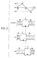
- Fig. 2 is a view illustrating the principles of a first embodiment according to the present invention, in which piezoelectric elements 13a and 13b are arranged on both sides of a movable portion 12 slidably mounted on a guide mechanism 11. Both elements are polarized in the same direction so that, for example, positive pole appears in the left end sides of both elements.
- a negative pole electrode of the piezoelectric element 13b on the right hand side thus arranged, for example, is grounded with a standard potential, and a constant voltage of an X(V), for example, is applied to a positive pole electrode of the other piezoelectric element 13a.
- the applied voltage is divided into an intermediate potential of an X/2 (V) which can be obtained by two resistors 14a and 14b having the same resistance value R.
- a driving voltage of a ⁇ X (V) is obtained on the basis of the driving signals derived from an amplifier 15.
- X/2 + ⁇ X (V) which is obtained by adding both of them by an adder 16, is applied between the respective remaining electrodes of the piezoelectric elements 13a and 13b.
- the driving voltage ⁇ X is varied according to the variation of driving signal
- the voltages applied between the electrodes on both sides of the respective two piezoelectric elements 13a and 13b are increased/decreased as center of X/2, respectively. Therefore, the applied potentials to the piezoelectric elements 13a and 13b are increased on one side and decreased on the other side, respectively. As a result, one of the piezoelectric elements 13a and 13b is extended while the other is contracted.
- Fig. 3 which shows the voltage variations
- the driving voltages ⁇ X are zero in an equilibrium state as in the cases (a), (c), and (e)
- the output of the adder 16 is an X/2 (V). Therefore, the same voltage of X/2 is applied to both piezoelectric elements 13a and 13b, respectively, so that each piezoelectric elements is extended by the same amount to cause the movable portion 12 to be positioned in the center.
- the output of the adder 16 is X/2 + ⁇ X (V), so that the X/2 + ⁇ X (V) is applied to the piezoelectric element 13b on the grounded side while a voltage of an X/2 - ⁇ X (V) is applied to the other piezoelectric element 13a.
- the piezoelectric elements 13a and 13b are symmetrically contracted and extended, respectively, by the amount corresponding to the ⁇ X (V) as the extension amount in the case of X/2 is made reference.
- only one amplifier 15 is used for varying the driving voltages applied to the two piezoelectric elements 13a and 13b each arranged on the right and left hand sides, respectively. It is therefore possible to reverse the extension and contraction of the piezoelectric elements 13a and 13b easily and highly precisely, hence enabling to realize the accurate driving of the movable portion 12. It may be possible to drive the movable portion 12 by reversing the left and right side relationship of the piezoelectric elements 13a and 13b to the movable portion 12 without changing the above-mentioned wiring. In this case, the driving direction of the movable portion 12 becomes opposite to the direction set forth above.
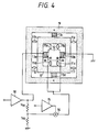
- Fig. 4 is a view showing the structure of the present embodiment, in which the same reference numerals in Fig. 2 designate the same members.
- the movable portion 12 which can be driven in the left and right hand directions of the drawing is arranged in the center of a first frame 17 by a guide mechanism comprising resilient hinge springs 11a, 11b, 11c and 11d.
- the piezoelectric elements 13a and 13b of a sensitivity 0.1(»m/V), for example, are arranged in the left and right side spaces between the movable portion 12 and the frame 17 so as to be extended ⁇ 5 (»m), respectively, each time a voltage of ⁇ 50 (V) is applied.
- each resistance value R of the resistors 14a and 14b is equal and is 10 k ⁇ , for example.
- the gain of the amplifier 15 is 10 times.
- a constant voltage X 100 (V) is applied by a high voltage amplifier 18.
- a second frame 19 is arranged outside the first frame 17, and the first frame 17 is supported by the second frame 19 through the guide mechanism comprising resilient hinge springs 11e, 11f, 11g and 11h so as to be movable in the vertical direction in Fig. 4.
- the frame 17 and the movable portion 12 can be driven relatively in the vertical direction in Fig. 4.
- the power supply circuit for driving the piezoelectric elements 13c and 13d are structured so as to be the same circuit as that shown in Fig. 4 to drive the piezoelectric elements 13a and 13b, but it is not shown in Fig. 4 to avoid any complication.
- the second frame 19 is fixedly arranged.
- the piezoelectric element 13a is extended by 4 (»m) and the piezoelectric element 13b by 6 (»m) from the initial length, respectively, thus enabling the movable portion 12 to be displaced from the center to the left side by one (1) (»m) against the frame 17.
- ⁇ X +10 (V)
- the output of the adder 16 becomes 40 (V). Consequently, the movable portion 12 is displaced from the center to the right side by one (1) (»m).
- the driving control is given to the piezoelectric elements 13c and 13d in the same manner to perform the fine movement of the movable portion 12 in the vertical direction.
- the position of the movable portion 12 can freely be controlled within a range of 5 (»m) from the center to the left and right sides and upper and lower sides each. To this end, it suffices if only the driving signal to be input into the amplifier 15 is varied within a range of -5 (V) to +5 (V). It is also possible to oscillate the movable portion 12 easily without any distortion by inputting triangular wave signals or sinusoidal wave signals.
- the resistance value for the resistors 14a and 14b is selected to the equal, but it may be possible to divide the resistance value unequally into 7:3 or the like so that the reference position is displaced from the center when the driving voltage ⁇ X is zero.
- Fig. 5 is a view illustrating a second embodiment according to the present invention.
- the present embodiment differs from the first embodiment in only a point that the high voltage amplifier 18 is replaced with a high voltage amplifier 18a capable of varying amplification and that an amplification factor controller 20 is newly provided to control the amplification factor of the amplifier 18a.
- the fluctuation will result in approximately ⁇ 10 (kgf) in terms of the preload and ⁇ 0.1 (»m) in terms of the displacement amount of the piezoelectric element.
- an adjustment can be made by varying the voltage applied to the electrode on the positive side of the piezoelectric element 13a by the high voltage amplifier 18a through the amplification factor controller 20 which is operated by a manufacturer of the apparatus. More specifically, with the fluctuation of approximately ⁇ 5 (V) the preload given to the piezoelectric elements can be adjusted to regulate the displacement amounts.
- the amplification factor is reduced by the controller 20 so that the voltage applied to the electrode on the positive side of the piezoelectric element 13a is reduced.
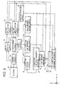
- Fig. 6 is a diagrammatic view showing the structure of the information recording and reproducing apparatus, in which a recording medium 22 is mounted on an x-y direction rough movement driving mechanism 21 to enable the rough movement within the x-y plane.
- a z-direction fine rough movements driving mechanism 23 is arranged above the medium 22.
- An x-y direction fine movement driving mechanism 24 is mounted on the driven portion of lower surface of the mechanism 23 to drivingly support a tangusten probe electrode 25 produced by an electrolytic polishing. The tip edge of the probe electrode 25 is placed close to the surface of the recording medium 22.
- the recording medium 22 is formed in such a manner that on a substrate 26 produced by polishing glass, a base electrode 27 is formed with gold (Au) on a chrome base layer by a vacuum deposition, and a recording layer 28 of graphite (HOPG) is bonded by a conductive adhesive agent thereon.
- the recording/reproducing area of the surface of the recording layer 28 is smoothed by cleavage in atomic order.
- an interface 29 which serves as a connection to upstream side apparatus of the information recording/reproducing apparatus is connected to the above-mentioned driving mechanisms, recording medium 22 and probe electrode 25 through the electric circuits given below.
- a control circuit 30 to perform central control of interrelated operations between the respective blocks in the information recording/reproducing apparatus; a write/readout circuit 31 to write or readout the write/readout data in accordance with command from the control circuit 30; a voltage application circuit 32 to write data by applying a pulse voltage between the probe electrode 25 and the base electrode 27 in accordance with signal from the write/readout circuit 31 or to apply a readout voltage when performing a readout; a voltage amplification circuit 33 to amplify the current flowing between the probe electrode 25 and recording medium 22 and to transmit this current to the write/readout circuit 31 as readout information signal when performing readout; a positioning circuit 34 to determine positions in the x-direction or y-direction in accordance with command from the control circuit 30 and others on the basis of signals from the voltage amplification circuit 33 or a position detecting circuit which will be described later; a servo circuit 35 to perform servo controls of the positions in the x-direction or y-direction on the basis
- the x-y direction fine movement driving mechanism 24 and the x-y direction fine movement driving circuit 37f are structured as shown in Fig. 4 or Fig. 5, and the command signals from the servo circuit 35 are input into the amplifier 15 of each circuit for x and y-direction drivings to perform the aforesaid driving controls.
- the probe electrode 25 is initially positioned slightly above the medium 22 in order to avoid any contact with the recording medium 22, and when in use, it is caused to be positioned close to the recording medium 22 by means of the z-direction rough movement driving mechanism 23.
- a 200 mV read voltage is applied by the voltage application circuit 32 between the probe electrode 25 and the base electrode 27 of the recording medium 22.
- the electrodes are caused to approach each other until the current being detected by the voltage amplification circuit 33 becomes 100 pA, and the z-direction fine/rough movements driving mechanism 23 is held.
- scanning is performed over the recording medium 22 to record information or reproduce recorded information.
- Recording is performed by applying the pulse voltage from the voltage application circuit 32 at write positions commanded by the control circuit 30 while the probe electrode 25 is caused to scan the recording area of the recording medium 22 line by line.
- This pulse voltage is 4 (V) of pulse height and one (1) (»s) of pulse width, which is a threshold value for which the portion of the graphite layer where a voltage is applied is changed into a concavity.
- Reproducing is performed by reading the change in current in the voltage amplification circuit 33 by scanning the recording area with the probe electrode 25 using the x-y direction fine movement driving mechanism 24 while a 200 (mV) readout voltage is being applied from the voltage application circuit 32 between the probe electrode 25 and base electrode 27.
- the above-mentioned apparatus is a recording/reproducing apparatus, but it is needless to mention that the apparatus can be either for recording or for reproducing only. It should be noted that the conditions required for writing and reading are not confined to the above-mentioned example. Also, the x-y direction fine movement driving circuit and x-y fine movement driving mechanism which are provided on the probe electrode side, may be arranged on the recording medium side.
Landscapes
- Physics & Mathematics (AREA)
- Health & Medical Sciences (AREA)
- General Health & Medical Sciences (AREA)
- General Physics & Mathematics (AREA)
- Nuclear Medicine, Radiotherapy & Molecular Imaging (AREA)
- Radiology & Medical Imaging (AREA)
- Control Of Position Or Direction (AREA)
- Signal Processing Not Specific To The Method Of Recording And Reproducing (AREA)
- Automatic Disk Changers (AREA)
- General Electrical Machinery Utilizing Piezoelectricity, Electrostriction Or Magnetostriction (AREA)
Claims (11)
- Antriebsvorrichtung zum Antrieb eines Objektes (12),
mit- einem ersten Paar piezoelektrischer Elemente (13a, 13b), wobei eines des Paares piezoelektrischer Elemente auf einer Seite des Objektes (12) und das andere des Paares piezoelektrischer Elemente auf der anderen Seite des Objektes angeordnet ist und jedes der piezoelektrischen Elemente eine innere und eine äußere Elektrode aufweist,- wobei jede Elektrodenanordnungsrichtung des Paares piezoelektrischer Elemente (13a, 13b) im wesentlichen identisch mit der anderen ist, und- einer ersten Steuerschaltung (14a, 14b, 15, 16; 18; 18a, 20), wobei die Steuerschaltung eine vorbestimmte Spannung zwischen die inneren und äußeren Elektroden des Paares piezoelektrischer Elemente anlegt und dadurch bewirkt, daß das Paar piezoelektrischer Elemente das Objekt (12) antreibt,dadurch gekennzeichnet, daß
die Steuerschaltung (14a, 14b, 15, 16; 18; 18a, 20) eine Variation der Werte des an die inneren Elektroden angelegten Potentials erlaubt. - Vorrichtung nach Anspruch 1, wobei
das der inneren Elektrode gegebene Potential durch Addition eines vorbestimmten Potentials zu einem mittleren Potential erhalten wird, welch letzteres durch Widerstandsteilung einer zwischen die äußeren Elektroden angelegten vorbestimmten Spannung erhalten wird. - Vorrichtung nach Anspruch 1 oder 2, wobei
jede Außenseite des Paares piezoelektrischer Elemente (13a, 13b) an einem Rahmenteil befestigt ist, welches das Objekt (12) umgibt. - Vorrichtung nach Anspruch 3,
die weiter ein Verbindungsglied (11a-11d) zur Verbindung des Rahmenteils (17, 19) und des Objektes (12) derart, daß es in der Richtung relativ bewegbar ist, aufweist. - Vorrichtung nach einem der Ansprüche 1 bis 4,
die weiter Mittel (14a, 14b) zum Einstellen der zwischen die äußeren Elektroden anzulegenden Spannung aufweist. - Vorrichtung nach einem der Ansprüche 1 bis 5
zum Antrieb eines Objektes, welche weiter aufweist:- ein Tragglied (17) zum Tragen des jeweils äußeren Abschnittes des ersten Paares piezoelektrischer Elemente (13a, 13b),- ein zweites Paar piezoelektrischer Elemente (13c, 13d), wobei eines des zweiten Paares piezoelektrischer Elemente auf einer Seite einer zweiten Richtung, die sich von der ersten Richtung des Traggliedes (17) unterscheidet, angeordnet ist und das andere des zweiten Paares piezoelektrischer Elemente in der zweiten Richtung auf der anderen Seite des Traggliedes angeordnet ist, wobei jede Elektrodenanordnungsrichtung des zweiten Paares piezoelektrischer Elemente (13c, 13d) im wesentlichen mit der zweiten Richtung übereinstimmt, und- eine zweite Steuerschaltung, wobei die zweite Steuerschaltung eine vorbestimmte Spannung zwischen die innere und die äußere Elektrode des zweiten Paares piezoelektrischer Elemente anlegt, wobei die zweite Steuerschaltung eine Variation des den inneren Elektroden verliehenen Potentials erlaubt, wodurch bewirkt wird, daß das zweite Paar piezoelektrischer Elemente (13c, 13d) das Tragglied (17) in die zweite Richtung antreibt, und weiter bewirkt wird, daß das Objekt (12) in die zweite Richtung angetrieben wird. - Vorrichtung nach Anspruch 6, wobei
jede Außenseite des zweiten Paares piezoelektrischer Elemente (13c, 13d) an einem Rahmenteil (19) befestigt ist, welches das Tragglied (17) umgibt. - Vorrichtung nach Anspruch 7,
die weiter ein Verbindungsglied (11e-11h) zum Verbinden des Rahmenteils (19) des Traggliedes (17) derart, daß dieses in die zweite Richtung bewegbar ist, aufweist. - Vorrichtung nach einem der Ansprüche 6 bis 8,
die weiter ein Verbindungsglied (11a-11d) zum Verbinden des Objektes (12) und des Traggliedes (17) derart, daß das Tragglied und das Objekt so verbunden sind, daß dieses in die erste Richtung bewegbar ist, aufweist. - Gerät zum Aufzeichnen und/oder Wiedergeben von Information auf ein/von einem Aufzeichnungsmedium, mit:- einem Tragglied zum Tragen des Aufzeichnungsmediums,- einer Sonde zum Aufzeichnen und/oder Wiedergeben von Information auf das/von dem Informationsaufzeichnungsmedium, das durch das Tragglied getragen wird, und- einer Anordnung, an der entweder das Tragglied oder die Sonde angebracht ist,dadurch gekennzeichnet, daß
die Anordnung entsprechend einem der Ansprüche 1 bis 9 ausgebildet ist. - Vorrichtung nach einem der Ansprüche 1 bis 10, bei der die Steuerschaltung (14a, 14b, 15, 16, 18, 18a, 20) jeder inneren Elektrode des Paares piezoelektrischer Elemente (13a, 13b, 13c, 13d) ein gleiches Potential verleiht.
Applications Claiming Priority (2)
| Application Number | Priority Date | Filing Date | Title |
|---|---|---|---|
| JP37746/91 | 1991-02-08 | ||
| JP3774691 | 1991-02-08 |
Publications (2)
| Publication Number | Publication Date |
|---|---|
| EP0499149A1 EP0499149A1 (de) | 1992-08-19 |
| EP0499149B1 true EP0499149B1 (de) | 1995-05-03 |
Family
ID=12506045
Family Applications (1)
| Application Number | Title | Priority Date | Filing Date |
|---|---|---|---|
| EP92102009A Expired - Lifetime EP0499149B1 (de) | 1991-02-08 | 1992-02-06 | Antriebsvorrichtung und Aufnahme- und Wiedergabegerät unter Verwendung derselben Vorrichtung |
Country Status (5)
| Country | Link |
|---|---|
| US (1) | US5297130A (de) |
| EP (1) | EP0499149B1 (de) |
| AT (1) | ATE122141T1 (de) |
| CA (1) | CA2060674C (de) |
| DE (1) | DE69202261T2 (de) |
Families Citing this family (34)
| Publication number | Priority date | Publication date | Assignee | Title |
|---|---|---|---|---|
| JP2895694B2 (ja) * | 1992-12-08 | 1999-05-24 | シャープ株式会社 | 情報記録・再生用スライダー、情報記録・再生用スライダーの製造方法および情報記録・再生装置 |
| US5751683A (en) * | 1995-07-24 | 1998-05-12 | General Nanotechnology, L.L.C. | Nanometer scale data storage device and associated positioning system |
| US6339217B1 (en) * | 1995-07-28 | 2002-01-15 | General Nanotechnology Llc | Scanning probe microscope assembly and method for making spectrophotometric, near-field, and scanning probe measurements |
| US6337479B1 (en) * | 1994-07-28 | 2002-01-08 | Victor B. Kley | Object inspection and/or modification system and method |
| US6507553B2 (en) | 1995-07-24 | 2003-01-14 | General Nanotechnology Llc | Nanometer scale data storage device and associated positioning system |
| JPH10105243A (ja) | 1996-09-10 | 1998-04-24 | Hewlett Packard Co <Hp> | 位置決め機構、位置決め装置及び情報記録装置 |
| JP3563247B2 (ja) | 1997-10-31 | 2004-09-08 | 日立建機株式会社 | 走査型プローブ顕微鏡 |
| US6802646B1 (en) * | 2001-04-30 | 2004-10-12 | General Nanotechnology Llc | Low-friction moving interfaces in micromachines and nanomachines |
| US6752008B1 (en) | 2001-03-08 | 2004-06-22 | General Nanotechnology Llc | Method and apparatus for scanning in scanning probe microscopy and presenting results |
| US6923044B1 (en) | 2001-03-08 | 2005-08-02 | General Nanotechnology Llc | Active cantilever for nanomachining and metrology |
| US7196328B1 (en) | 2001-03-08 | 2007-03-27 | General Nanotechnology Llc | Nanomachining method and apparatus |
| US6787768B1 (en) | 2001-03-08 | 2004-09-07 | General Nanotechnology Llc | Method and apparatus for tool and tip design for nanomachining and measurement |
| US6297937B1 (en) * | 1998-02-24 | 2001-10-02 | Seagate Technology Llc | Suspension with adjustable preload |
| DE19902413C1 (de) * | 1999-01-22 | 2000-05-31 | Daimler Chrysler Ag | Verfahren zur Kalibrierung eines piezoelektrischen Stellantriebes |
| AU6061100A (en) * | 1999-07-01 | 2001-01-22 | General Nanotechnology, Llc | Object inspection and/or modification system and method |
| US6931710B2 (en) * | 2001-01-30 | 2005-08-23 | General Nanotechnology Llc | Manufacturing of micro-objects such as miniature diamond tool tips |
| US7253407B1 (en) | 2001-03-08 | 2007-08-07 | General Nanotechnology Llc | Active cantilever for nanomachining and metrology |
| US7053369B1 (en) | 2001-10-19 | 2006-05-30 | Rave Llc | Scan data collection for better overall data accuracy |
| US6813937B2 (en) | 2001-11-28 | 2004-11-09 | General Nanotechnology Llc | Method and apparatus for micromachines, microstructures, nanomachines and nanostructures |
| WO2004023490A2 (en) | 2002-09-09 | 2004-03-18 | General Nanotechnology Llc | Fluid delivery for scanning probe microscopy |
| JP3792675B2 (ja) * | 2003-06-05 | 2006-07-05 | ファナック株式会社 | 微細位置決め装置及び工具補正方法 |
| JP2005004921A (ja) * | 2003-06-13 | 2005-01-06 | Alps Electric Co Ltd | 高精度位置決め装置 |
| DE102004011724B4 (de) * | 2004-02-06 | 2006-08-10 | Physik Instrumente (Pi) Gmbh & Co. Kg | Miniaturisierte Zweiachsen-Piezo-Betätigungseinrichtung |
| JP2007171021A (ja) * | 2005-12-22 | 2007-07-05 | Canon Inc | 走査プローブ装置及び走査プローブ装置用の駆動ステージ |
| US8001831B2 (en) * | 2007-05-31 | 2011-08-23 | Sii Nano Technology Inc. | Positioning apparatus and scanning probe microscope employing the same |
| DE102008049647B4 (de) * | 2008-09-30 | 2011-11-24 | Technische Universität Dresden | Mikromechanisches Element und Verfahren zum Betreiben eines mikromechanischen Elements |
| CN105094147B (zh) * | 2014-04-23 | 2017-12-19 | 中国科学院物理研究所 | 精密致动装置 |
| CN103990998B (zh) * | 2014-05-20 | 2017-01-25 | 广东工业大学 | 基于应力刚化原理的刚度频率可调二维微动平台 |
| GB2539869A (en) * | 2015-05-07 | 2017-01-04 | Elektron Tech Uk Ltd | Nanopositioner |
| CN107833594B (zh) * | 2017-09-13 | 2020-02-21 | 南京航空航天大学 | 一种用于高精度定位和测量的二维三自由度微动平台结构 |
| US10564553B2 (en) * | 2017-09-26 | 2020-02-18 | Guangdong University Of Technology | Large load-bearing guide mechanism and multi-DOF large-stroke high-precision motion platform system |
| US12025788B2 (en) * | 2021-05-06 | 2024-07-02 | The Regents Of The University Of California | System and method for simultaneous longitudinal biological imaging |
| CN114512579B (zh) * | 2022-02-18 | 2022-10-11 | 广东工业大学 | 一种Mini/micro芯片柔性飞行刺晶装置 |
| CN119028899B (zh) * | 2024-08-16 | 2025-12-19 | 广东工业大学 | 位移解耦并联驱动柔性铰链二维平台 |
Family Cites Families (14)
| Publication number | Priority date | Publication date | Assignee | Title |
|---|---|---|---|---|
| US3786332A (en) * | 1969-03-19 | 1974-01-15 | Thomson Houston Comp Francaise | Micro positioning apparatus |
| US4169276A (en) * | 1977-10-17 | 1979-09-25 | Ampex Corporation | Drive circuit for controlling a movable magnetic head |
| GB2179212B (en) * | 1985-08-13 | 1989-05-10 | Marconi Co Ltd | Bimorph drive circuit |
| US4798989A (en) * | 1986-09-26 | 1989-01-17 | Research Development Corporation | Scanning tunneling microscope installed in electron microscope |
| EP0292562A4 (de) * | 1986-12-03 | 1990-05-14 | Jgc Corp | Antriebseinheit und motoranordnung unter verwendung dieser einheit. |
| US4841191A (en) * | 1987-02-20 | 1989-06-20 | Hitachi, Ltd. | Piezoelectric actuator control apparatus |
| JPH01287403A (ja) * | 1988-05-16 | 1989-11-20 | Nippon Telegr & Teleph Corp <Ntt> | 走査型トンネル顕微鏡 |
| JP2896794B2 (ja) * | 1988-09-30 | 1999-05-31 | キヤノン株式会社 | 走査型トンネル電流検出装置,走査型トンネル顕微鏡,及び記録再生装置 |
| JP2547869B2 (ja) * | 1988-11-09 | 1996-10-23 | キヤノン株式会社 | プローブユニット,該プローブの駆動方法及び該プローブユニットを備えた走査型トンネル電流検知装置 |
| JPH0625642B2 (ja) * | 1988-11-29 | 1994-04-06 | 工業技術院長 | 走査型トンネル顕微鏡装置 |
| JPH02240977A (ja) * | 1989-03-14 | 1990-09-25 | Toshiba Corp | 変位発生装置 |
| JP2686645B2 (ja) * | 1989-05-08 | 1997-12-08 | キヤノン株式会社 | 走査型トンネル電流検出装置 |
| US5075548A (en) * | 1989-07-17 | 1991-12-24 | Olympus Optical Co., Ltd. | Tunnel current probe moving mechanism having parallel cantilevers |
| US4992659A (en) * | 1989-07-27 | 1991-02-12 | International Business Machines Corporation | Near-field lorentz force microscopy |
-
1992
- 1992-02-05 CA CA002060674A patent/CA2060674C/en not_active Expired - Lifetime
- 1992-02-06 EP EP92102009A patent/EP0499149B1/de not_active Expired - Lifetime
- 1992-02-06 DE DE69202261T patent/DE69202261T2/de not_active Expired - Lifetime
- 1992-02-06 AT AT92102009T patent/ATE122141T1/de not_active IP Right Cessation
- 1992-02-07 US US07/832,595 patent/US5297130A/en not_active Expired - Lifetime
Also Published As
| Publication number | Publication date |
|---|---|
| CA2060674C (en) | 1996-10-01 |
| ATE122141T1 (de) | 1995-05-15 |
| CA2060674A1 (en) | 1992-08-09 |
| EP0499149A1 (de) | 1992-08-19 |
| DE69202261T2 (de) | 1995-11-23 |
| DE69202261D1 (de) | 1995-06-08 |
| US5297130A (en) | 1994-03-22 |
Similar Documents
| Publication | Publication Date | Title |
|---|---|---|
| EP0499149B1 (de) | Antriebsvorrichtung und Aufnahme- und Wiedergabegerät unter Verwendung derselben Vorrichtung | |
| US5412641A (en) | Information recording/reproducing apparatus for recording/reproducing information with probes | |
| US5107112A (en) | Scanning tunnel-current-detecting device and method for detecting tunnel current and scanning tunnelling microscope and recording/reproducing device using thereof | |
| US5220555A (en) | Scanning tunnel-current-detecting device and method for detecting tunnel current and scanning tunnelling microscope and recording/reproducing device using thereof | |
| US5043577A (en) | Distance-controlled tunneling transducer | |
| EP0534406B1 (de) | Mechanismus zum parallelen Halten einer Fläche und Apparat zur Verwendung eines solchen Mechanismus | |
| EP0391429B1 (de) | Vorrichtung zur Erfassung von Mikroverschiebungen, Piezo-Stellantrieb unter Verwendung der Vorrichtung und Abtastmikroskop unter Verwendung des Piezo-Stellantriebes | |
| US5717680A (en) | Information processing apparatus with mechanism for adjusting interval between substrate for supporting a plurality of probes and recording medium | |
| US4169276A (en) | Drive circuit for controlling a movable magnetic head | |
| JPH04157640A (ja) | 情報記録担体及びこれを使用する情報処理装置 | |
| JP2744346B2 (ja) | 情報記録ユニットと情報記録及び/又は再生装置と情報記録及び/又は再生方法と情報記録媒体 | |
| EP0452851B1 (de) | Informationsaufzeichnungs-und Wiedergabegerät | |
| US5371727A (en) | Scanning tunnel microscopy information processing system with noise detection to correct the tracking mechanism | |
| US5210714A (en) | Distance-controlled tunneling transducer and direct access storage unit employing the transducer | |
| GB2235052A (en) | Tunnel current probe moving mechanism having parallel cantilevers | |
| USRE36603E (en) | Distance-controlled tunneling transducer and direct access storage unit employing the transducer | |
| JP3105987B2 (ja) | 微動装置及びそれを用いた情報記録及び/又は再生装置 | |
| JPH0250333A (ja) | 記録再生装置 | |
| JP3126527B2 (ja) | 情報処理装置 | |
| JP3053971B2 (ja) | トンネル電流発生用三次元変位素子、該トンネル電流発生用三次元変位素子を用いたマルチ探針ユニット、および情報処理装置 | |
| JP3023901B2 (ja) | 情報記録再生装置 | |
| JPH07191756A (ja) | 微動駆動装置及びそれを用いた情報記録及び/又は再生装置 | |
| NL1000815C2 (nl) | XY-verplaatsingsinrichting. | |
| JP3313757B2 (ja) | 粗動微動機構 | |
| JP2962612B2 (ja) | 走査顕微鏡 |
Legal Events
| Date | Code | Title | Description |
|---|---|---|---|
| PUAI | Public reference made under article 153(3) epc to a published international application that has entered the european phase |
Free format text: ORIGINAL CODE: 0009012 |
|
| AK | Designated contracting states |
Kind code of ref document: A1 Designated state(s): AT BE CH DE DK ES FR GB GR IT LI LU MC NL PT SE |
|
| 17P | Request for examination filed |
Effective date: 19921221 |
|
| 17Q | First examination report despatched |
Effective date: 19940124 |
|
| GRAA | (expected) grant |
Free format text: ORIGINAL CODE: 0009210 |
|
| AK | Designated contracting states |
Kind code of ref document: B1 Designated state(s): AT BE CH DE DK ES FR GB GR IT LI LU MC NL PT SE |
|
| PG25 | Lapsed in a contracting state [announced via postgrant information from national office to epo] |
Ref country code: IT Free format text: LAPSE BECAUSE OF FAILURE TO SUBMIT A TRANSLATION OF THE DESCRIPTION OR TO PAY THE FEE WITHIN THE PRESCRIBED TIME-LIMIT;WARNING: LAPSES OF ITALIAN PATENTS WITH EFFECTIVE DATE BEFORE 2007 MAY HAVE OCCURRED AT ANY TIME BEFORE 2007. THE CORRECT EFFECTIVE DATE MAY BE DIFFERENT FROM THE ONE RECORDED. Effective date: 19950503 Ref country code: GR Free format text: LAPSE BECAUSE OF FAILURE TO SUBMIT A TRANSLATION OF THE DESCRIPTION OR TO PAY THE FEE WITHIN THE PRESCRIBED TIME-LIMIT Effective date: 19950503 Ref country code: LI Effective date: 19950503 Ref country code: NL Free format text: LAPSE BECAUSE OF FAILURE TO SUBMIT A TRANSLATION OF THE DESCRIPTION OR TO PAY THE FEE WITHIN THE PRESCRIBED TIME-LIMIT Effective date: 19950503 Ref country code: MC Free format text: LAPSE BECAUSE OF NON-PAYMENT OF DUE FEES Effective date: 19950503 Ref country code: CH Effective date: 19950503 Ref country code: BE Effective date: 19950503 Ref country code: AT Effective date: 19950503 Ref country code: ES Free format text: THE PATENT HAS BEEN ANNULLED BY A DECISION OF A NATIONAL AUTHORITY Effective date: 19950503 Ref country code: DK Effective date: 19950503 |
|
| REF | Corresponds to: |
Ref document number: 122141 Country of ref document: AT Date of ref document: 19950515 Kind code of ref document: T |
|
| REF | Corresponds to: |
Ref document number: 69202261 Country of ref document: DE Date of ref document: 19950608 |
|
| PG25 | Lapsed in a contracting state [announced via postgrant information from national office to epo] |
Ref country code: SE Effective date: 19950803 Ref country code: PT Effective date: 19950803 |
|
| ET | Fr: translation filed | ||
| REG | Reference to a national code |
Ref country code: CH Ref legal event code: PL |
|
| NLV1 | Nl: lapsed or annulled due to failure to fulfill the requirements of art. 29p and 29m of the patents act | ||
| PG25 | Lapsed in a contracting state [announced via postgrant information from national office to epo] |
Ref country code: LU Free format text: LAPSE BECAUSE OF NON-PAYMENT OF DUE FEES Effective date: 19960229 |
|
| PLBE | No opposition filed within time limit |
Free format text: ORIGINAL CODE: 0009261 |
|
| STAA | Information on the status of an ep patent application or granted ep patent |
Free format text: STATUS: NO OPPOSITION FILED WITHIN TIME LIMIT |
|
| 26N | No opposition filed | ||
| REG | Reference to a national code |
Ref country code: GB Ref legal event code: IF02 |
|
| PGFP | Annual fee paid to national office [announced via postgrant information from national office to epo] |
Ref country code: FR Payment date: 20090223 Year of fee payment: 18 |
|
| PGFP | Annual fee paid to national office [announced via postgrant information from national office to epo] |
Ref country code: GB Payment date: 20100219 Year of fee payment: 19 Ref country code: DE Payment date: 20100228 Year of fee payment: 19 |
|
| REG | Reference to a national code |
Ref country code: FR Ref legal event code: ST Effective date: 20101029 |
|
| PG25 | Lapsed in a contracting state [announced via postgrant information from national office to epo] |
Ref country code: FR Free format text: LAPSE BECAUSE OF NON-PAYMENT OF DUE FEES Effective date: 20100301 |
|
| GBPC | Gb: european patent ceased through non-payment of renewal fee |
Effective date: 20110206 |
|
| REG | Reference to a national code |
Ref country code: DE Ref legal event code: R119 Ref document number: 69202261 Country of ref document: DE Effective date: 20110901 |
|
| PG25 | Lapsed in a contracting state [announced via postgrant information from national office to epo] |
Ref country code: GB Free format text: LAPSE BECAUSE OF NON-PAYMENT OF DUE FEES Effective date: 20110206 |
|
| PG25 | Lapsed in a contracting state [announced via postgrant information from national office to epo] |
Ref country code: DE Free format text: LAPSE BECAUSE OF NON-PAYMENT OF DUE FEES Effective date: 20110901 |