EP0499986A2 - Multilayer wiring structure and method for forming multilayer construction - Google Patents
Multilayer wiring structure and method for forming multilayer construction Download PDFInfo
- Publication number
- EP0499986A2 EP0499986A2 EP92102530A EP92102530A EP0499986A2 EP 0499986 A2 EP0499986 A2 EP 0499986A2 EP 92102530 A EP92102530 A EP 92102530A EP 92102530 A EP92102530 A EP 92102530A EP 0499986 A2 EP0499986 A2 EP 0499986A2
- Authority
- EP
- European Patent Office
- Prior art keywords
- thermal
- low
- polyimide
- expansivity
- film
- Prior art date
- Legal status (The legal status is an assumption and is not a legal conclusion. Google has not performed a legal analysis and makes no representation as to the accuracy of the status listed.)
- Granted
Links
- 0 C*(CC*)CCC(C*1C*(*2)C2C1)C(C)(C)*(*)* Chemical compound C*(CC*)CCC(C*1C*(*2)C2C1)C(C)(C)*(*)* 0.000 description 4
- NAXSWNILAQOXOP-UHFFFAOYSA-N c1c2OOOc2cc(-c(cc2)cc3c2OOO3)c1 Chemical compound c1c2OOOc2cc(-c(cc2)cc3c2OOO3)c1 NAXSWNILAQOXOP-UHFFFAOYSA-N 0.000 description 1
Images

Classifications
-
- H—ELECTRICITY
- H05—ELECTRIC TECHNIQUES NOT OTHERWISE PROVIDED FOR
- H05K—PRINTED CIRCUITS; CASINGS OR CONSTRUCTIONAL DETAILS OF ELECTRIC APPARATUS; MANUFACTURE OF ASSEMBLAGES OF ELECTRICAL COMPONENTS
- H05K3/00—Apparatus or processes for manufacturing printed circuits
- H05K3/46—Manufacturing multilayer circuits
-
- H—ELECTRICITY
- H05—ELECTRIC TECHNIQUES NOT OTHERWISE PROVIDED FOR
- H05K—PRINTED CIRCUITS; CASINGS OR CONSTRUCTIONAL DETAILS OF ELECTRIC APPARATUS; MANUFACTURE OF ASSEMBLAGES OF ELECTRICAL COMPONENTS
- H05K3/00—Apparatus or processes for manufacturing printed circuits
- H05K3/46—Manufacturing multilayer circuits
- H05K3/4644—Manufacturing multilayer circuits by building the multilayer layer by layer, i.e. build-up multilayer circuits
- H05K3/4652—Adding a circuit layer by laminating a metal foil or a preformed metal foil pattern
- H05K3/4655—Adding a circuit layer by laminating a metal foil or a preformed metal foil pattern by using a laminate characterized by the insulating layer
-
- H—ELECTRICITY
- H05—ELECTRIC TECHNIQUES NOT OTHERWISE PROVIDED FOR
- H05K—PRINTED CIRCUITS; CASINGS OR CONSTRUCTIONAL DETAILS OF ELECTRIC APPARATUS; MANUFACTURE OF ASSEMBLAGES OF ELECTRICAL COMPONENTS
- H05K1/00—Printed circuits
- H05K1/02—Details
- H05K1/03—Use of materials for the substrate
- H05K1/0313—Organic insulating material
- H05K1/032—Organic insulating material consisting of one material
- H05K1/0346—Organic insulating material consisting of one material containing N
-
- H—ELECTRICITY
- H05—ELECTRIC TECHNIQUES NOT OTHERWISE PROVIDED FOR
- H05K—PRINTED CIRCUITS; CASINGS OR CONSTRUCTIONAL DETAILS OF ELECTRIC APPARATUS; MANUFACTURE OF ASSEMBLAGES OF ELECTRICAL COMPONENTS
- H05K3/00—Apparatus or processes for manufacturing printed circuits
- H05K3/46—Manufacturing multilayer circuits
- H05K3/4644—Manufacturing multilayer circuits by building the multilayer layer by layer, i.e. build-up multilayer circuits
- H05K3/4673—Application methods or materials of intermediate insulating layers not specially adapted to any one of the previous methods of adding a circuit layer
-
- H—ELECTRICITY
- H05—ELECTRIC TECHNIQUES NOT OTHERWISE PROVIDED FOR
- H05K—PRINTED CIRCUITS; CASINGS OR CONSTRUCTIONAL DETAILS OF ELECTRIC APPARATUS; MANUFACTURE OF ASSEMBLAGES OF ELECTRICAL COMPONENTS
- H05K3/00—Apparatus or processes for manufacturing printed circuits
- H05K3/46—Manufacturing multilayer circuits
- H05K3/4644—Manufacturing multilayer circuits by building the multilayer layer by layer, i.e. build-up multilayer circuits
- H05K3/4673—Application methods or materials of intermediate insulating layers not specially adapted to any one of the previous methods of adding a circuit layer
- H05K3/4676—Single layer compositions
-
- H—ELECTRICITY
- H10—SEMICONDUCTOR DEVICES; ELECTRIC SOLID-STATE DEVICES NOT OTHERWISE PROVIDED FOR
- H10W—GENERIC PACKAGES, INTERCONNECTIONS, CONNECTORS OR OTHER CONSTRUCTIONAL DETAILS OF DEVICES COVERED BY CLASS H10
- H10W70/00—Package substrates; Interposers; Redistribution layers [RDL]
- H10W70/60—Insulating or insulated package substrates; Interposers; Redistribution layers
- H10W70/67—Insulating or insulated package substrates; Interposers; Redistribution layers characterised by their insulating layers or insulating parts
- H10W70/69—Insulating materials thereof
-
- H—ELECTRICITY
- H05—ELECTRIC TECHNIQUES NOT OTHERWISE PROVIDED FOR
- H05K—PRINTED CIRCUITS; CASINGS OR CONSTRUCTIONAL DETAILS OF ELECTRIC APPARATUS; MANUFACTURE OF ASSEMBLAGES OF ELECTRICAL COMPONENTS
- H05K2201/00—Indexing scheme relating to printed circuits covered by H05K1/00
- H05K2201/01—Dielectrics
- H05K2201/0137—Materials
- H05K2201/0154—Polyimide
-
- H—ELECTRICITY
- H05—ELECTRIC TECHNIQUES NOT OTHERWISE PROVIDED FOR
- H05K—PRINTED CIRCUITS; CASINGS OR CONSTRUCTIONAL DETAILS OF ELECTRIC APPARATUS; MANUFACTURE OF ASSEMBLAGES OF ELECTRICAL COMPONENTS
- H05K2201/00—Indexing scheme relating to printed circuits covered by H05K1/00
- H05K2201/01—Dielectrics
- H05K2201/0183—Dielectric layers
- H05K2201/0195—Dielectric or adhesive layers comprising a plurality of layers, e.g. in a multilayer structure
-
- H—ELECTRICITY
- H05—ELECTRIC TECHNIQUES NOT OTHERWISE PROVIDED FOR
- H05K—PRINTED CIRCUITS; CASINGS OR CONSTRUCTIONAL DETAILS OF ELECTRIC APPARATUS; MANUFACTURE OF ASSEMBLAGES OF ELECTRICAL COMPONENTS
- H05K2201/00—Indexing scheme relating to printed circuits covered by H05K1/00
- H05K2201/06—Thermal details
- H05K2201/068—Thermal details wherein the coefficient of thermal expansion is important
-
- H—ELECTRICITY
- H05—ELECTRIC TECHNIQUES NOT OTHERWISE PROVIDED FOR
- H05K—PRINTED CIRCUITS; CASINGS OR CONSTRUCTIONAL DETAILS OF ELECTRIC APPARATUS; MANUFACTURE OF ASSEMBLAGES OF ELECTRICAL COMPONENTS
- H05K2203/00—Indexing scheme relating to apparatus or processes for manufacturing printed circuits covered by H05K3/00
- H05K2203/07—Treatments involving liquids, e.g. plating, rinsing
- H05K2203/0756—Uses of liquids, e.g. rinsing, coating, dissolving
- H05K2203/0759—Forming a polymer layer by liquid coating, e.g. a non-metallic protective coating or an organic bonding layer
-
- H—ELECTRICITY
- H05—ELECTRIC TECHNIQUES NOT OTHERWISE PROVIDED FOR
- H05K—PRINTED CIRCUITS; CASINGS OR CONSTRUCTIONAL DETAILS OF ELECTRIC APPARATUS; MANUFACTURE OF ASSEMBLAGES OF ELECTRICAL COMPONENTS
- H05K3/00—Apparatus or processes for manufacturing printed circuits
- H05K3/46—Manufacturing multilayer circuits
- H05K3/4644—Manufacturing multilayer circuits by building the multilayer layer by layer, i.e. build-up multilayer circuits
-
- H—ELECTRICITY
- H05—ELECTRIC TECHNIQUES NOT OTHERWISE PROVIDED FOR
- H05K—PRINTED CIRCUITS; CASINGS OR CONSTRUCTIONAL DETAILS OF ELECTRIC APPARATUS; MANUFACTURE OF ASSEMBLAGES OF ELECTRICAL COMPONENTS
- H05K3/00—Apparatus or processes for manufacturing printed circuits
- H05K3/46—Manufacturing multilayer circuits
- H05K3/4644—Manufacturing multilayer circuits by building the multilayer layer by layer, i.e. build-up multilayer circuits
- H05K3/4652—Adding a circuit layer by laminating a metal foil or a preformed metal foil pattern
-
- Y—GENERAL TAGGING OF NEW TECHNOLOGICAL DEVELOPMENTS; GENERAL TAGGING OF CROSS-SECTIONAL TECHNOLOGIES SPANNING OVER SEVERAL SECTIONS OF THE IPC; TECHNICAL SUBJECTS COVERED BY FORMER USPC CROSS-REFERENCE ART COLLECTIONS [XRACs] AND DIGESTS
- Y10—TECHNICAL SUBJECTS COVERED BY FORMER USPC
- Y10T—TECHNICAL SUBJECTS COVERED BY FORMER US CLASSIFICATION
- Y10T29/00—Metal working
- Y10T29/49—Method of mechanical manufacture
- Y10T29/49002—Electrical device making
- Y10T29/49117—Conductor or circuit manufacturing
- Y10T29/49124—On flat or curved insulated base, e.g., printed circuit, etc.
- Y10T29/49126—Assembling bases
-
- Y—GENERAL TAGGING OF NEW TECHNOLOGICAL DEVELOPMENTS; GENERAL TAGGING OF CROSS-SECTIONAL TECHNOLOGIES SPANNING OVER SEVERAL SECTIONS OF THE IPC; TECHNICAL SUBJECTS COVERED BY FORMER USPC CROSS-REFERENCE ART COLLECTIONS [XRACs] AND DIGESTS
- Y10—TECHNICAL SUBJECTS COVERED BY FORMER USPC
- Y10T—TECHNICAL SUBJECTS COVERED BY FORMER US CLASSIFICATION
- Y10T29/00—Metal working
- Y10T29/49—Method of mechanical manufacture
- Y10T29/49002—Electrical device making
- Y10T29/49117—Conductor or circuit manufacturing
- Y10T29/49124—On flat or curved insulated base, e.g., printed circuit, etc.
- Y10T29/49128—Assembling formed circuit to base
-
- Y—GENERAL TAGGING OF NEW TECHNOLOGICAL DEVELOPMENTS; GENERAL TAGGING OF CROSS-SECTIONAL TECHNOLOGIES SPANNING OVER SEVERAL SECTIONS OF THE IPC; TECHNICAL SUBJECTS COVERED BY FORMER USPC CROSS-REFERENCE ART COLLECTIONS [XRACs] AND DIGESTS
- Y10—TECHNICAL SUBJECTS COVERED BY FORMER USPC
- Y10T—TECHNICAL SUBJECTS COVERED BY FORMER US CLASSIFICATION
- Y10T29/00—Metal working
- Y10T29/49—Method of mechanical manufacture
- Y10T29/49002—Electrical device making
- Y10T29/49117—Conductor or circuit manufacturing
- Y10T29/49124—On flat or curved insulated base, e.g., printed circuit, etc.
- Y10T29/49155—Manufacturing circuit on or in base
- Y10T29/49163—Manufacturing circuit on or in base with sintering of base
-
- Y—GENERAL TAGGING OF NEW TECHNOLOGICAL DEVELOPMENTS; GENERAL TAGGING OF CROSS-SECTIONAL TECHNOLOGIES SPANNING OVER SEVERAL SECTIONS OF THE IPC; TECHNICAL SUBJECTS COVERED BY FORMER USPC CROSS-REFERENCE ART COLLECTIONS [XRACs] AND DIGESTS
- Y10—TECHNICAL SUBJECTS COVERED BY FORMER USPC
- Y10T—TECHNICAL SUBJECTS COVERED BY FORMER US CLASSIFICATION
- Y10T428/00—Stock material or miscellaneous articles
- Y10T428/31504—Composite [nonstructural laminate]
- Y10T428/31721—Of polyimide
Definitions
- This invention relates to a multilayer wiring structure featuring use of a polyimide for the insulating layer. More particularly, the invention pertains to a multilayer wiring structure which is reduced in thermal stress by use of a low-thermal-expansivity polyimide for the layer insulating films and also has high bonding reliability between conductor/insulating film or insulating film/conductor or at the interface between the insulating films.
- Polyimide resins are used as material of layer insulating films for multilayer wiring boards as said resins are excellent in heat resistance, chemical resistance and insulating properties and low in dielectric constant.
- the conventional polyimides when used for forming the layer insulating films, present the problem of cracking or imperfect adhesion due to build-up of thermal stress after heat curing, that is, the stress caused by the difference in thermal expansion coefficient between the substrate or wiring material and the polyimide.
- a low-thermal-expansivity polyimide having a thermal expansion coefficient of 2 x 10 ⁇ 5 K ⁇ 1 or less, which is close to that of the substrate or wiring material, owing to its rod-like structure as disclosed in Japanese Patent Application Kokai (Laid-Open) No. 61-176196.
- a film or layer of a material is formed directly (without applying any treatment) on an insulating layer using a perfectly cured low-thermal-expansivity polyimide, there could take place exfoliation at the interface between the insulating layers or between the insulating layer and wiring metal, and thus there arises the problem of reliability.
- Japanese Patent Application Kokai No. H1-245586 discloses use of a flexible printed board in which the insulator consists of a layer of a high-thermal-expansivity resin contacting the conductor and a layer of a low-thermal-expansivity resin contacting the first-said resin layer for improving adhesiveness between the conductor and the insulator.
- multilayer wiring boards having multilayer wiring comprising a plural number of insulating film layers and a plural number of conductor patterns, such as wiring boards for modules, multilayer flexible printed boards, LSI multilayer wiring boards, etc.
- high adhesiveness is required not only for conductor/polyimide interface but also for substrate/polyimide and polyimide/polyimide interfaces, so that it was necessary to take a measure that can satisfy both requirements for low-thermal-expansivity and high adhesiveness at various interfaces.
- FEP perfluoroethylene-perfluoropropylene copolymer
- the object of the present invention is to accomplish multilayer wiring with high reliability by improving adhesiveness at various interfaces applied with polyimide while maintaining low thermal expansivity when forming a multilayer wiring structure using a low-thermal-expansivity polyimide.
- a multilayer construction in which a flexible and highly adhesive thin insulating film is disposed on the upper and lower sides of the low-thermal-expansivity polymer layers and the conductor pattern layers, thereby making it possible to offer a multilayer wiring structure with high reliability.
- the multilayer wiring board comprises a substrate 1, a highly adhesive and flexible polyimide thin film 2, a low-thermal-expansivity polyimide 3, a highly adhesive and flexible polyimide thin film 4, metallic wiring 5, a highly adhesive polyimide thin film 6, and a low-thermal-expansivity polyimide 7.
- a multilayer wiring structure comprising a plural number of conductor pattern layers and a plural number of low-thermal expansivity polymer insulating film layers, characterized in that the coefficient of thermal expansion of the low-thermal-expansivity polymer constituting the insulating films is 2 x 10 ⁇ 5 K ⁇ 1 to 4 x 10 ⁇ 6 K ⁇ 1, and a film of a polyimide with a flexible skeleton having at least one highly flexible bond in the main chain is formed on the upper and lower sides of said conductor pattern layers and said low-thermal-expansivity polymer insulating film layers.
- Low-thermal-expansivity polyimides, aromatic heterocyclic polymers and the like are usable for forming said low-thermal-expansivity polymer insulating films in the present invention.
- the flexible and highly adhesive polyimide film (the above-mentioned film of a polyimide with a flexible skeleton) is most preferably used in a half-cured state, but in case it is necessary to form a metallic wiring pattern layer on a perfectly or fully cured film, wiring is applied on a perfectly cured interface-modified film, followed by formation thereon of a highly adhesive thin film of polyimide, and then an insulating film of a low-thermal-expansivity polymer is further formed thereon.
- a multilayer wiring structure comprising a plural number of conductor pattern layers and a plural number of low-thermal-expansivity polymer insulating film layers, characterized in that a polymer film is formed on the upper and lower sides of said conductor pattern layers and said layers of insulating films, that the peel strength of bond between the conductor pattern layer or insulating film of low-thermal-expansivity polymer and said polyimide film is 200 - 1,000 g/cm, and that heat resistance of said polyimide film is such that the weight loss starting temperature of said polyimide film in the air is 400 - 600°C.
- multilayer flexible printed boards, high-density multilayer wiring boards and semiconductor devices utilizing a multilayer wiring structure having a construction in which a flexible and highly adhesive thin insulating film is disposed on the upper and lower sides of the low-thermal-expansivity polymer layers and the conductor pattern layers.
- the low-thermal-expansivity layer is made of a polymer having a thermal expansion coefficient of 2 x 10 ⁇ 5 K ⁇ 1 to 4 x 10 ⁇ 6 K ⁇ 1 at temperatures of 50-200°C and a value of Khun's segment of 90 or more. Measurement of the value is described in T.M. Birshtein, Polymer Science USSR, 19 , 63, (1977), and T.M. Birshtein, V.A. Zubov, I.S. Milevskaya, V.E. Eskin, I.A. Baranovskaya, M.M. Koton, V.V. Kudryavtsev, and V.P. Sklizzkova, Europe Polymer Journal, 13 , 375, (1977).
- polystyrene resin Typical examples of such polymers are aromatic heterocyclic polymers such as polyimide, polybenzimidazole, polybenzoxazole, polybenzthiazole, polypyrrolone and the like.
- the polyimide has, for example, chemical structural units represented by the following formula: and/or
- the low-thermal-expansivity polyimide used in this invention is composed of the structural units of the formula: and/or wherein R is selected from C1 ⁇ 6 alkyl group, fluorinated C1 ⁇ 6 alkyl group, C1 ⁇ 6 alkoxyl group, fluorinated C1 ⁇ 6 alkoxyl group, C1 ⁇ 6 acyl group and halogen; 1 is an integer of 0 to 4; m is an integer of 0 to 2; and n is an integer of 0 to 3.
- the structural unit of the polyimide molecule is selected from those of the following formulae: wherein R is selected from alkyl group, fluorinated alkyl group, alkoxyl group, fluorinated alkoxyl group, acyl group and halogen as heretofore defined; k is an integer of 0 to 3; 1 is an integer of 0 to 4; m is an integer of 0 to 2; and n is an integer of 0 to 3.
- This polyimide may be blended or copolymerized with other polymer(s).
- polymer(s) there may be used a copolymer of polyimide and polyamide, and a blend of polyimide with polyamide, polybenzoxazole, polybenzothiazole or polypyrrolone.
- the polyimide having such a skeleton can be obtained from single polymerization of an aromatic diaminocarboxylic acid derivative or from reaction of an aromatic diamine or an aromatic diisocyanate and an aromatic tetracarboxylic acid derivative.
- the tetracarboxylic acid derivatives usable in the above reaction include esters, acid anhydrides and acid chlorides. Use of an acid anhydride is preferred from the viewpoint of synthesis.
- the synthesis reaction is usually carried out in a solvent such as N-methylpyrrolidone, dimethylformamide, dimethylacetamide, dimethyl sulfoxide, dimethyl sulfate, sulforan, butyrolactone, cresol, phenol, phenol halide, cyclohexane, dioxane and the like at a temperature in the range of 0 to 200°C.
- the diaminocarboxylic acid derivatives usable for said polymerization in this invention include 4-aminophthalic acid, 4-amino-5-methylphthalic acid, 4-(p-anilino)phthalic acid, 4-(3,5-dimethyl-4-anilino)phthalic acid and the like as well as their esters, acid anhydrides and acid chlorides.
- aromatic diamines usable for said reaction in this invention include p-phenylenediamine, 2,5-diaminotoluene, 2,5-diaminoxylene, diaminodurene(2,3,5,6-tetramethyl-p-phenylenediamine), 2,5-diaminobenzotrifluoride, 2,5-diaminoanisole, 2,5-diaminoacetophenone, 2,5-diaminobenzophenone, 2,5-diaminodiphenyl, 2,5-diaminofluorobenzene, benzidine, o-tolidine, m-tolidine, 3,3'-dimethoxybenzidine, 3,3',5,5'-tetramethylbenzidine, 3,3'-di(trifluoromethyl)benzidine, 3,3'-diacetylbenzidine, 3,3'-difluorobenzidine, octafluorobenzidine, 4,4'-d
- the diisocyanate compounds of the above diamines can be used as well.
- the tetracarboxylic acid derivatives usable in the above reaction include pyromellitic acid, methylpyromellitic acid, dimethylpyromellitic acid, di(trifluoromethyl)pyromellitic acid, 3,3',4,4'-biphenyltetracarboxylic acid, p-(3,4-dicarboxyphenyl)benzene, and their acid anhydrides, acid chlorides and esters.
- a diaminosiloxane represented by the formula: (wherein R1 and R3 are a monovalent organic group, R2 and R4 are a divalent organic group, and p and q are an integer greater than 1) may be used as part of the aromatic diamine.
- the highly adhesive thin film according to this invention is a film of a polymer with a flexible skeleton having at least one highly flexible bond -Ar-X-Ar- (X being a divalent organic group with high flexibility) in the main chain and capable of fully exhibiting inherent high heat resistance of low-thermal-expansivity polyimide.
- the polymer is selected from the polyimides composed of benzoxazole resin, benzothiazole resin, maleimide resin and the following monomers: aromatic diamines such as 4,4'-diaminodiphenyl ether, 4,4'-diaminodiphenylsulfone, 4,4'-diaminodiphenylmethane, 4,4'-diaminodiphenyl sulfide, 4,4'-diaminodicyclohexylmethane, 4,4'-bis(paraaminophenoxy)biphenyl, 4,4'-bis(methaaminophenoxy)diphenylsulfone, 2,2'-bis(4-(paraaminophenoxy)phenyl)propane, 3,3'-dimethyl-4,4'-diaminodiphenylmethane, 2,2'-bis(4-(paraaminophenoxy)phenyl)hexafluoropropane, 4,
- Such a polymer can be obtained from single polymerization of an aromatic diaminocarboxylic acid derivative or from reaction of an aromatic diamine or an aromatic diisocyanate and an aromatic tetracarboxylic acid derivative.
- the thickness of the highly adhesive thin film is less than 20% of the thickness of the low-thermal-expansivity polyimide film.
- the polyimide used for the highly adhesive thin film has a large coefficient of thermal expansion owing to the flexible skeleton of the main chain. Therefore, increase of the amount of the highly adhesive thin film present in the insulating layer may result in loss of low thermal expansivity of the polyimide film as a whole, so that it is desirable that said thin film is as small in thickness as possible.
- the film of a polyimide having a flexible skeleton when the upper layer is formed after the lower layer has been perfectly hardened, shows far higher adhesion than between the films of a low-thermal-expansivity polyimide having a rod-like structure. This is considered attributable to the fact that the polyimide having a flexible skeleton is more likely to develop entanglement of molecules than the polyimide having a rod-like skeleton and tends to form a thick diffusion layer. Therefore, adhesion between the insulating layers can be enhanced by forming an interface of the flexible polyimide films at the interface of the low-thermal-expansivity polyimide films. Low thermal expansivity of the multilayered film as a whole can be maintained by controlling the thickness of the flexible polymer film to be less than 20% of the thickness of the low-thermal-expansivity polyimide film.
- a thin polyimide film 2 having flexibility is formed on a substrate 1.
- the polyimide for forming the interface modifying film there was used a varnish of a polyamide acid obtained by reacting 1 mole of an aromatic diamine shown below and 1 mole of an aromatic tetracarboxylic acid dianhydride shown below in N-methylpyrrolidone.
- the warnish is spin coated on the substrate and cured first at 100°C for one hour and then at 200°C for 30 minutes (into a half-cured state) to form a 0.5-1 ⁇ m thick film.
- a low-thermal-expansivity polyimide layer 3 is formed as shown in Fig. 2(b).
- the low-thermal-expansivity polyimide there was used a varnish of a polyamide acid obtained by reacting 1 mole of p-PDA (p-phenylenediamine) and 1 mole of s-BPDA (3,3',4,4'-biphenyltetracarboxylic acid dianhydride) in NMP, and this varnish was spin coated on the substrate to form a 10-20 ⁇ m thick film of a half-cured state.
- a flexible polyimide thin film 4 is formed (film thickness: 0.5-1 ⁇ m) by curing the coating at 100°C for one hour and then at 350°C for 30 minutes (into a perfectly cured state), followed by application of metallic wiring 5.
- Said flexible polyimide thin film was formed from a varnish obtained by using 1 mole of DDE as diamine and 1 mole of s-BPDA as acid dianhydride.
- an interface modifying thin film 6 (0.5-1 ⁇ m thick) is again formed in a half-cured state from 1 mole of a diamine shown below and 1 mole of an acid dianhydride shown below, and a low-thermal-expansivity polyimide film 7 (10-20 ⁇ m thick) is further formed thereon in a half-cured state.
- Fig. 1 shows an example of trial manufacture of a high-density multilayer wiring board using a highly adhesive polyimide shown in Example 1.
- the curing temperature was raised to 400°C to perfectly imidate the three layers at the same time.
- the steps of (a) and (b) were repeated to form a 10-layer wiring board.
- the respective wiring layers were connected by a connecting pedestal.
- Each wiring layer was about 5 ⁇ m thick and the pedestal had a thickness of about 10 ⁇ m.
- the present invention it is possible to provide a multilayer wiring structure with high reliability in which a low-thermal-expansivity polyimide is used for forming the layer insulating films and adhesion between the low-thermal-expansivity polyimide film and the wiring pattern layer is improved.
Landscapes
- Engineering & Computer Science (AREA)
- Microelectronics & Electronic Packaging (AREA)
- Manufacturing & Machinery (AREA)
- Production Of Multi-Layered Print Wiring Board (AREA)
- Laminated Bodies (AREA)
- Macromolecular Compounds Obtained By Forming Nitrogen-Containing Linkages In General (AREA)
- Polymers With Sulfur, Phosphorus Or Metals In The Main Chain (AREA)
Abstract
Description
- This invention relates to a multilayer wiring structure featuring use of a polyimide for the insulating layer. More particularly, the invention pertains to a multilayer wiring structure which is reduced in thermal stress by use of a low-thermal-expansivity polyimide for the layer insulating films and also has high bonding reliability between conductor/insulating film or insulating film/conductor or at the interface between the insulating films.
- Polyimide resins are used as material of layer insulating films for multilayer wiring boards as said resins are excellent in heat resistance, chemical resistance and insulating properties and low in dielectric constant. However, the conventional polyimides, when used for forming the layer insulating films, present the problem of cracking or imperfect adhesion due to build-up of thermal stress after heat curing, that is, the stress caused by the difference in thermal expansion coefficient between the substrate or wiring material and the polyimide. For avoiding this problem, it is desirable to use a polyimide having a thermal expansion coefficient as close to that of the substrate or wiring material as possible. For instance, it is effective to apply, for forming the insulating films, a low-thermal-expansivity polyimide having a thermal expansion coefficient of 2 x 10⁻⁵ K⁻¹ or less, which is close to that of the substrate or wiring material, owing to its rod-like structure as disclosed in Japanese Patent Application Kokai (Laid-Open) No. 61-176196. However, when a film or layer of a material is formed directly (without applying any treatment) on an insulating layer using a perfectly cured low-thermal-expansivity polyimide, there could take place exfoliation at the interface between the insulating layers or between the insulating layer and wiring metal, and thus there arises the problem of reliability. As a method for solving such a problem, Japanese Patent Application Kokai No. H1-245586 discloses use of a flexible printed board in which the insulator consists of a layer of a high-thermal-expansivity resin contacting the conductor and a layer of a low-thermal-expansivity resin contacting the first-said resin layer for improving adhesiveness between the conductor and the insulator. However, in the multilayer wiring boards having multilayer wiring comprising a plural number of insulating film layers and a plural number of conductor patterns, such as wiring boards for modules, multilayer flexible printed boards, LSI multilayer wiring boards, etc., high adhesiveness is required not only for conductor/polyimide interface but also for substrate/polyimide and polyimide/polyimide interfaces, so that it was necessary to take a measure that can satisfy both requirements for low-thermal-expansivity and high adhesiveness at various interfaces.
- As a method for laminating a polyimide with low adhesiveness, use of FEP (perfluoroethylene-perfluoropropylene copolymer) as a heat-fusible adhesive is proposed in Japanese Patent Application Kokai No. 57-83432. However, FEP is lower in heat resistance (especially in softening point and melting point) than polyimides and can not provide satisfactory heat resistance.
- Also, the idea of laminating the cured polyimide films by using a half-cured polyamic acid film is proposed in Japanese Patent Publication No. 57-5229, but little improvement of adhesiveness is admitted with the perfectly cured low-thermal-expansivity polyimide.
- It is known that silicon-modified polyimides such as disclosed in Japanese Patent Application Kokai No. 62-227963 are enhanced in adhesiveness to glass or silicon substrates. However, in case a low-thermal-expansivity polyimide film is formed on a cured silicon-modified low-thermal-expansivity polyimide film, there is the problem that adhesion between the polyimide insulating films is low.
- Thus, in forming the multilayer wiring boards of the type in which there exists various types of interfaces, it was impossible with the conventional techniques to satisfy both requirements for high adhesion at all interfaces and low thermal expansivity at the same time.
- As described above, it was difficult to form a multilayer wiring structure by using a low-thermal-expansivity polyimide for the layer insulating films.
- The object of the present invention is to accomplish multilayer wiring with high reliability by improving adhesiveness at various interfaces applied with polyimide while maintaining low thermal expansivity when forming a multilayer wiring structure using a low-thermal-expansivity polyimide.
- For attaining said object, there is provided a multilayer construction in which a flexible and highly adhesive thin insulating film is disposed on the upper and lower sides of the low-thermal-expansivity polymer layers and the conductor pattern layers, thereby making it possible to offer a multilayer wiring structure with high reliability.
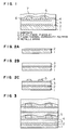
- The essentials of the present invention are described hereinafter with reference to the accompanying drawings wherein:
- Fig. 1 is a sectional view of a high-density multilayer wiring board;
- Figs. 2 (a)-(c) are the sectional views showing the process of manufacturing a multilayer wiring structure;
- Fig. 3 is a sectional view of a high-density multilayer wiring board having a plurality of wirings; and
- Figs. 4(a) and (b) are the sectional views showing the measurement of peel strength.
- In Fig. 1, the multilayer wiring board comprises a substrate 1, a highly adhesive and flexible polyimide
thin film 2, a low-thermal-expansivity polyimide 3, a highly adhesive and flexible polyimidethin film 4,metallic wiring 5, a highly adhesive polyimide thin film 6, and a low-thermal-expansivity polyimide 7. - In a first aspect of the present invention, there is provided a multilayer wiring structure comprising a plural number of conductor pattern layers and a plural number of low-thermal expansivity polymer insulating film layers, characterized in that the coefficient of thermal expansion of the low-thermal-expansivity polymer constituting the insulating films is 2 x 10⁻⁵ K⁻¹ to 4 x 10⁻⁶ K⁻¹, and a film of a polyimide with a flexible skeleton having at least one highly flexible bond in the main chain is formed on the upper and lower sides of said conductor pattern layers and said low-thermal-expansivity polymer insulating film layers. Low-thermal-expansivity polyimides, aromatic heterocyclic polymers and the like are usable for forming said low-thermal-expansivity polymer insulating films in the present invention. The flexible and highly adhesive polyimide film (the above-mentioned film of a polyimide with a flexible skeleton) is most preferably used in a half-cured state, but in case it is necessary to form a metallic wiring pattern layer on a perfectly or fully cured film, wiring is applied on a perfectly cured interface-modified film, followed by formation thereon of a highly adhesive thin film of polyimide, and then an insulating film of a low-thermal-expansivity polymer is further formed thereon.
- In a second aspect of this invention, there is provided a multilayer wiring structure comprising a plural number of conductor pattern layers and a plural number of low-thermal-expansivity polymer insulating film layers, characterized in that a polymer film is formed on the upper and lower sides of said conductor pattern layers and said layers of insulating films, that the peel strength of bond between the conductor pattern layer or insulating film of low-thermal-expansivity polymer and said polyimide film is 200 - 1,000 g/cm, and that heat resistance of said polyimide film is such that the weight loss starting temperature of said polyimide film in the air is 400 - 600°C.
- In a third aspect of the present invention, there is provided a method for producing a multilayer wiring structure having a construction in which a flexible and highly adhesive thin insulating film is disposed on the upper and lower sides of the low-thermal-expansivity polymer layers and the conductor pattern layers.
- In a fourth aspect of the present invention, there are provided multilayer flexible printed boards, high-density multilayer wiring boards and semiconductor devices utilizing a multilayer wiring structure having a construction in which a flexible and highly adhesive thin insulating film is disposed on the upper and lower sides of the low-thermal-expansivity polymer layers and the conductor pattern layers.
- In the present invention, the low-thermal-expansivity layer is made of a polymer having a thermal expansion coefficient of 2 x 10⁻⁵ K⁻¹ to 4 x 10⁻⁶ K⁻¹ at temperatures of 50-200°C and a value of Khun's segment of 90 or more. Measurement of the value is described in T.M. Birshtein, Polymer Science USSR, 19, 63, (1977), and T.M. Birshtein, V.A. Zubov, I.S. Milevskaya, V.E. Eskin, I.A. Baranovskaya, M.M. Koton, V.V. Kudryavtsev, and V.P. Sklizzkova, Europe Polymer Journal, 13, 375, (1977).
- Typical examples of such polymers are aromatic heterocyclic polymers such as polyimide, polybenzimidazole, polybenzoxazole, polybenzthiazole, polypyrrolone and the like. The polyimide has, for example, chemical structural units represented by the following formula:

and/or
- The low-thermal-expansivity polyimide used in this invention is composed of the structural units of the formula:

and/or
wherein R is selected from C₁₋₆ alkyl group, fluorinated C₁₋₆ alkyl group, C₁₋₆ alkoxyl group, fluorinated C₁₋₆ alkoxyl group, C₁₋₆ acyl group and halogen; 1 is an integer of 0 to 4; m is an integer of 0 to 2; and n is an integer of 0 to 3. - The structural unit of the polyimide molecule is selected from those of the following formulae:


wherein R is selected from alkyl group, fluorinated alkyl group, alkoxyl group, fluorinated alkoxyl group, acyl group and halogen as heretofore defined; k is an integer of 0 to 3; 1 is an integer of 0 to 4; m is an integer of 0 to 2; and n is an integer of 0 to 3. - This polyimide may be blended or copolymerized with other polymer(s). For example, there may be used a copolymer of polyimide and polyamide, and a blend of polyimide with polyamide, polybenzoxazole, polybenzothiazole or polypyrrolone.
- The polyimide having such a skeleton can be obtained from single polymerization of an aromatic diaminocarboxylic acid derivative or from reaction of an aromatic diamine or an aromatic diisocyanate and an aromatic tetracarboxylic acid derivative.
- The tetracarboxylic acid derivatives usable in the above reaction include esters, acid anhydrides and acid chlorides. Use of an acid anhydride is preferred from the viewpoint of synthesis. The synthesis reaction is usually carried out in a solvent such as N-methylpyrrolidone, dimethylformamide, dimethylacetamide, dimethyl sulfoxide, dimethyl sulfate, sulforan, butyrolactone, cresol, phenol, phenol halide, cyclohexane, dioxane and the like at a temperature in the range of 0 to 200°C.
- The diaminocarboxylic acid derivatives usable for said polymerization in this invention include 4-aminophthalic acid, 4-amino-5-methylphthalic acid, 4-(p-anilino)phthalic acid, 4-(3,5-dimethyl-4-anilino)phthalic acid and the like as well as their esters, acid anhydrides and acid chlorides.
- The aromatic diamines usable for said reaction in this invention include p-phenylenediamine, 2,5-diaminotoluene, 2,5-diaminoxylene, diaminodurene(2,3,5,6-tetramethyl-p-phenylenediamine), 2,5-diaminobenzotrifluoride, 2,5-diaminoanisole, 2,5-diaminoacetophenone, 2,5-diaminobenzophenone, 2,5-diaminodiphenyl, 2,5-diaminofluorobenzene, benzidine, o-tolidine, m-tolidine, 3,3'-dimethoxybenzidine, 3,3',5,5'-tetramethylbenzidine, 3,3'-di(trifluoromethyl)benzidine, 3,3'-diacetylbenzidine, 3,3'-difluorobenzidine, octafluorobenzidine, 4,4'-diaminoterphenyl and 4,4'-diaminooctaphenyl.
- The diisocyanate compounds of the above diamines can be used as well.
- The tetracarboxylic acid derivatives usable in the above reaction include pyromellitic acid, methylpyromellitic acid, dimethylpyromellitic acid, di(trifluoromethyl)pyromellitic acid, 3,3',4,4'-biphenyltetracarboxylic acid, p-(3,4-dicarboxyphenyl)benzene, and their acid anhydrides, acid chlorides and esters.
- For improving adhesion to the substrate made of Si, SiO₂, Al, SiN or the like, a diaminosiloxane represented by the formula:
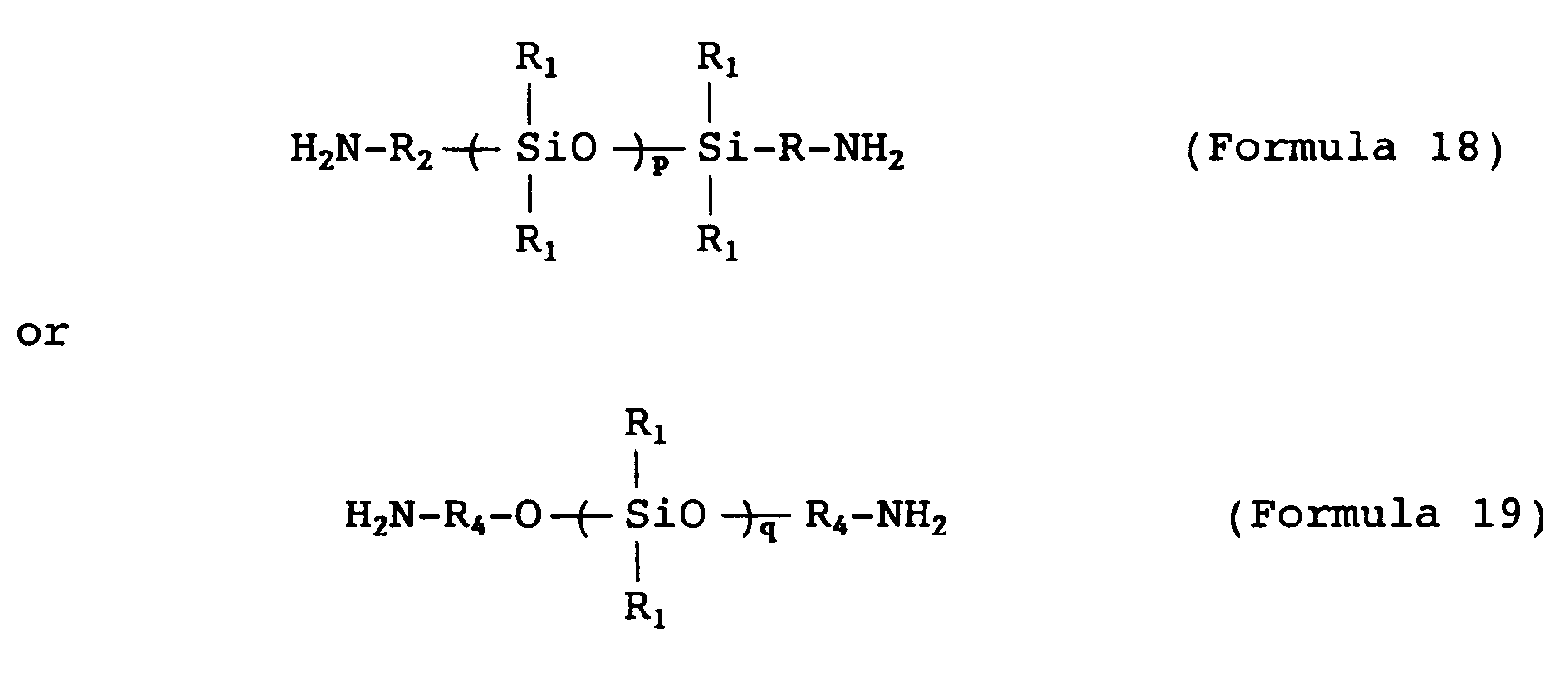
(wherein R₁ and R₃ are a monovalent organic group, R₂ and R₄ are a divalent organic group, and p and q are an integer greater than 1) may be used as part of the aromatic diamine. - The highly adhesive thin film according to this invention is a film of a polymer with a flexible skeleton having at least one highly flexible bond -Ar-X-Ar- (X being a divalent organic group with high flexibility) in the main chain and capable of fully exhibiting inherent high heat resistance of low-thermal-expansivity polyimide. The polymer is selected from the polyimides composed of benzoxazole resin, benzothiazole resin, maleimide resin and the following monomers: aromatic diamines such as 4,4'-diaminodiphenyl ether, 4,4'-diaminodiphenylsulfone, 4,4'-diaminodiphenylmethane, 4,4'-diaminodiphenyl sulfide, 4,4'-diaminodicyclohexylmethane, 4,4'-bis(paraaminophenoxy)biphenyl, 4,4'-bis(methaaminophenoxy)diphenylsulfone, 2,2'-bis(4-(paraaminophenoxy)phenyl)propane, 3,3'-dimethyl-4,4'-diaminodiphenylmethane, 2,2'-bis(4-(paraaminophenoxy)phenyl)hexafluoropropane, 4,4'-diaminobenzophenone, 4,4'-bis(paraaminophenoxy)diphenylsulfone and 4,4'-dithiodianiline; acid dianhydrides such as 3,3',4,4'-benzophenonetetracarboxylic acid dianhydride, 2,2-bis(4-(3,4-dicarboxyphenoxy)phenyl)propanoic acid dianhydride, 2,2-bis(4-(3,4-dicarboxyphenoxy)phenyl)hexafluoropropanoic acid dianhydride, 3,3',4,4'-diphenylethertetracarboxylic acid dianhydride, 3,3',4,4'-diphenylsulfonetetracarboxylic acid dianhydride, 2,2-bis(3,4-dicarboxyphenyl)propanoic acid dianhydride and 2,2-bis(3,4-dicarboxyphenyl)hexafluoropropanoic acid dianhydride. In case of using an aromatic diamine such as mentioned above, pyromellitic acid dianhydride or 3,3',4,4'-biphenyltetracarboxylic acid dianhydride may be used as acid dianhydride.
- Such a polymer can be obtained from single polymerization of an aromatic diaminocarboxylic acid derivative or from reaction of an aromatic diamine or an aromatic diisocyanate and an aromatic tetracarboxylic acid derivative.
- In the present invention, it is essential that the thickness of the highly adhesive thin film is less than 20% of the thickness of the low-thermal-expansivity polyimide film. The polyimide used for the highly adhesive thin film has a large coefficient of thermal expansion owing to the flexible skeleton of the main chain. Therefore, increase of the amount of the highly adhesive thin film present in the insulating layer may result in loss of low thermal expansivity of the polyimide film as a whole, so that it is desirable that said thin film is as small in thickness as possible.
- The film of a polyimide having a flexible skeleton, when the upper layer is formed after the lower layer has been perfectly hardened, shows far higher adhesion than between the films of a low-thermal-expansivity polyimide having a rod-like structure. This is considered attributable to the fact that the polyimide having a flexible skeleton is more likely to develop entanglement of molecules than the polyimide having a rod-like skeleton and tends to form a thick diffusion layer. Therefore, adhesion between the insulating layers can be enhanced by forming an interface of the flexible polyimide films at the interface of the low-thermal-expansivity polyimide films. Low thermal expansivity of the multilayered film as a whole can be maintained by controlling the thickness of the flexible polymer film to be less than 20% of the thickness of the low-thermal-expansivity polyimide film.
- The examples of the present invention will be described stepwise below with reference to the accompanying drawings.
- As shown in Fig. 2(a), a
thin polyimide film 2 having flexibility is formed on a substrate 1. As the polyimide for forming the interface modifying film, there was used a varnish of a polyamide acid obtained by reacting 1 mole of an aromatic diamine shown below and 1 mole of an aromatic tetracarboxylic acid dianhydride shown below in N-methylpyrrolidone.
- The warnish is spin coated on the substrate and cured first at 100°C for one hour and then at 200°C for 30 minutes (into a half-cured state) to form a 0.5-1 µm thick film.
- Then a low-thermal-
expansivity polyimide layer 3 is formed as shown in Fig. 2(b). As the low-thermal-expansivity polyimide, there was used a varnish of a polyamide acid obtained by reacting 1 mole of p-PDA (p-phenylenediamine) and 1 mole of s-BPDA (3,3',4,4'-biphenyltetracarboxylic acid dianhydride) in NMP, and this varnish was spin coated on the substrate to form a 10-20 µm thick film of a half-cured state. - Further, as shown in Fig. 2(c), a flexible polyimide
thin film 4 is formed (film thickness: 0.5-1 µm) by curing the coating at 100°C for one hour and then at 350°C for 30 minutes (into a perfectly cured state), followed by application ofmetallic wiring 5. Said flexible polyimide thin film was formed from a varnish obtained by using 1 mole of DDE as diamine and 1 mole of s-BPDA as acid dianhydride. - Thereafter, as shown in Fig. 1, an interface modifying thin film 6 (0.5-1 µm thick) is again formed in a half-cured state from 1 mole of a diamine shown below and 1 mole of an acid dianhydride shown below, and a low-thermal-expansivity polyimide film 7 (10-20 µm thick) is further formed thereon in a half-cured state.

- Peel strength was measured by a peeling test using the samples shown in Figure 4. These samples were fabricated as follows:
- (1) Sample A for polyimide coated on SiO₂. Polyamic acid varnish, spincoated on the thermally oxidized Si wafer, was converted to polyimide at 400°C for A2 and at 350°C for the others for 30 min. (Figure 4(a)).
- (2) Sample B for polyimide-polyimide interface on full cured polyimides; Aluminum chelate solution as an adhesion promoter was used on the substrate before spin coating of polyamic acid to form the first layer. Gold thin film was deposited on part of the first layer as a delamination layer. The second layer was fabricated by spin coating and thermal imidization on the first layer. The curing conditions for both layers were the same as for sample A. A Cr and Cu layer was deposited as the reinforcement layer for the peeling test (Figure 4(b)).
- (3) Sample C for polyimide-polyimide interface on semi cured polyimides. The polyimide first layer was fabricated by spin coating on aluminum-chelate solution-applied substrate. Thermal imidization was done at temperatures between 150 and 300°C for 30 min. Other steps were the same as for sample B.
- Fig. 1 shows an example of trial manufacture of a high-density multilayer wiring board using a highly adhesive polyimide shown in Example 1.
- On the surface of a 1 mm thick, 100 mm² alumina substrate 1 was deposited a thin copper film 8. (a) After applying and hardening a resist, a pattern was formed, and after forming a
first wiring layer 5 by electroplating, the resist was removed. (b) The polyimide precursor varnish of Example 1 was spin coated thereon and the coat was cured in a nitrogen atmosphere at 200°C for 30 minutes to form an about 1 µm thickflexible polyimide film 2. (c) On this film was similarly formed a low-thermal-expansivity polyimide film 3 with a thickness of about 20 µm. (d) Further formed thereon, in the similar way, was an about 1 µmthick polyimide film 4, the same as formed in Example 1. -

-

- In this step, the curing temperature was raised to 400°C to perfectly imidate the three layers at the same time. Thereafter, the steps of (a) and (b) were repeated to form a 10-layer wiring board. The respective wiring layers were connected by a connecting pedestal. Each wiring layer was about 5 µm thick and the pedestal had a thickness of about 10 µm.
- According to the present invention, it is possible to provide a multilayer wiring structure with high reliability in which a low-thermal-expansivity polyimide is used for forming the layer insulating films and adhesion between the low-thermal-expansivity polyimide film and the wiring pattern layer is improved.

Claims (17)
- A multilayer wiring structure comprising a plural number of conductor pattern layers (5) and a plural number of low-thermal-expansivity polyimide insulating film layers (3, 7), wherein the coefficient of thermal expansion of the low-thermal-expansivity polymer forming the insulating films is 2 x 10⁻⁵ K⁻¹ to 4 x 10⁻⁶ K⁻¹, and a film of a polyimide (2, 4, 6) with a flexible skeleton having at least one high-flexibility bond in the main chain is formed on the upper and lower side of said low-thermal-expansivity polymer insulating film layers (3, 7) and said conductor pattern layers.
- A multilayer wiring structure according to Claim 1, wherein the low-thermal-expansivity polymer (3, 7) is polyimide.
- A multilayer wiring structure comprising a plural number of conductor pattern layers (5) and a plural number of low-thermal-expansivity polymer insulating film layers (3, 7), wherein a polymer film (2, 4, 6) is formed on the upper and lower side of said conductor pattern layers (5) and said low-thermal expansivity polymer insulating film layers (3, 7), the peel strength of bond between a conductor pattern layer (5) or a low-thermal-expansivity polymer insulating film layer (3, 7) and said polymer film (2, 4, 6) is 200 - 1,000 g/cm, and heat resistance of said polymer film (2, 4, 6) is such that its weight loss starting temperature in the air is 400 - 600°C.
- A multilayer wiring structure comprising a plural number of conductor pattern layers (5) and a plural number of low-thermal-expansivity polyimide insulating film layers (3, 7), wherein a flexible polymer coating film (2, 4, 6) is formed on the upper and lower sides of the conductor pattern layers (5) and the low-thermal-expansivity polyimide insulating film layers (3, 7), the peel strength of bond between a conductor pattern layer (5) or a low-thermal-expansivity polyimide layer (3, 7) and said polymer coating film (2, 4, 6) is 200 - 1,000 g/cm, and heat resistance of said polymer coating film (2, 4, 6) is such that its weight loss starting temperature in the air is 400 - 600°C.
- A multilayer wiring structure comprising a plural number of conductor pattern layers (5) and a plural number of low-thermal-expansivity polyimide insulating film layers (3, 7), wherein a flexible polyimide coating film (2, 4, 6) is formed on the upper and the lower sides of the conductor pattern layers (5) and low-thermal-expansivity polyimide insulating film layers, (3, 7) the peel strength of bond between a conductor pattern layer (5) or a low-thermal-expansivity polyimide insulating film layer (3, 7) and said polyimide coating film (2, 4, 6) is 200 - 1,000 g/cm, and the thickness of said polyimide coating film (2, 4, 6) is 20% or less of the thickness of the low-thermal-expansivity polyimide insulating film (3, 7).
- A multilayer wiring structure comprising a plural number of conductor pattern layers (5) and a plural number of low-thermal-expansivity polyimide insulating film layers (3, 7), wherein the coefficient of thermal expansion of each low-thermal-expansivity polyimide insulating film (3, 7) is 2 x 10⁻⁵ K⁻¹ to 4 x 10⁻⁶ K⁻¹, a heterocyclic polymer film (2, 4, 6) is formed on the upper and lower sides of the low-thermal-expansivity polyimide insulating film layers (3, 7), the peel strength of bond between the low-thermal-expansivity polyimide film (3, 7) and the heterocyclic polymer film (2, 4, 6) is 200 - 1,000 g/cm, and the weight loss starting temperature of said heterocyclic polymer film (2, 4, 6) in the air is 400 - 600°C.
- A multilayer wiring structure comprising a plural number of conductor pattern layers (5) and a plural number of low-thermal-expansivity polyimide insulating film layers (3, 7), wherein a coating film of a polymer (2, 4, 6) having in its main chain at least one highly flexible bond of the following formula:

- A multilayer wiring structure comprising a plural number of conductor pattern layers (5) and a plural number of low-thermal-expansivity polyimide insulating film layers, (3, 7) wherein said low-thermal-expansivity polyimide insulating film layers (3, 7) are made of a polyimide having in its chemical structure at least one aromatic ring which is easily rotatable about the molecular axis but has no degree of freedom in other directions and also having as its chemical structural units the aromatic groups presenting linearity in the range of 0 ± 40°C around the molecular axis, said polyimide being oriented in at least one axial direction with an order parameter of 0.07 or greater, and a flexible polymer coating film (2, 4, 6) is formed on the upper and lower sides of said conductor pattern layers (5) and said low-thermal-expansivity polyimide layers (3, 7).
- A multilayer wiring structure comprising a plural number of conductor pattern layers (5) and a plural number of low-thermal-expansivity polyimide insulating film layers (3, 7), wherein said low-thermal-expansivity polyimide insulating films (3, 7) are made of a polyimide having the chemical structural units represented by the formula:
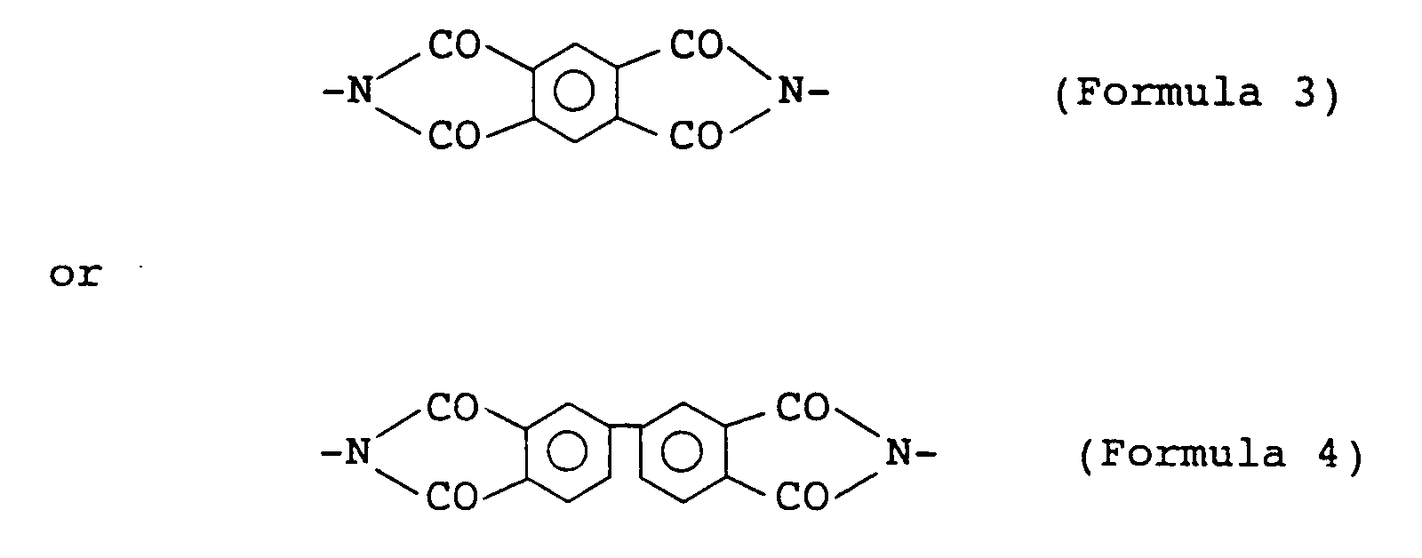

- A method for producing a multilayer wiring structure comprising a plural number of conductor pattern layers (5) and a plural number of low-thermal-expansivity polyimide insulating film layers (3, 7), which method comprises the steps of:(A) coating a flexible polymer varnish on a substrate (1) and heat-curing part of the polymer coating;(B) applying on said polymer coating a polyamic acid varnish which is a low-thermal-expansivity polyimide precursor and partly forming a polyimide (3) by conducting a thermal condensation reaction;(C) applying on said polyimide a flexible polymer varnish and heating it to form a flexible polymer film (4);(D) bonding a copper foil on said flexible polymer film and etching said copper foil layer to form a conductor pattern layer (5);(E) coating a flexible polymer varnish on said conductor pattern layer (5) and heat curing the polymer coating (6);(F) applying on said polymer coating a polyamic acid varnish which is a low-thermal-expansivity polyimide precursor and subjecting the precursor to a thermal condensation reaction to form a polyimide layer (7);(G) coating a flexible polymer varnish on the low-thermal-expansivity polyimide layer and heating the coating to form a polymer film; and
repeating the steps (D)-(E)-(F)-(G) at least once. - A method for producing a multilayer wiring structure comprising a plural number of conductor pattern layers (5) and a plural number of low-thermal-expansivity polyimide insulating film layers (3, 7), which method comprises the steps of:(A) depositing a thin copper film on a substrate (1);(B) applying and hardening a resist on said thin copper film and etching it to form a pattern;(C) forming a conductor pattern (5) by electro-plating of a metal and removing the resist;(D) coating a flexible polymer varnish on said conductor pattern layer (5) and heat curing the polymer coating to form a polymer coating film (6);(E) applying on said polymer coating film a varnish of polyamic acid which is a low-thermal-expansivity polyimide precursor, and subjecting the precursor to a thermal condensation reaction to form a polyimide layer;(F) coating a flexible polymer varnish on the low-thermal-expansivity polyimide film and heating the coating to form a polymer coating film;(G) depositing a thin copper film on said polymer coating film; and
repeating the steps (B)-(C)-(D)-(E)-(F)-(G) at least once. - A method for producing a multilayer wiring structure comprising a plural number of conductor pattern layers (5) and a plural number of low-thermal-expansivity polyimide insulating film layers (3, 7), which method comprises the steps of:(A) depositing a thin copper film on a substrate (1);(B) applying and hardening a resist on the thin copper film and etching it to form a thin film pattern;(C) coating thereon a flexible polymer varnish and heat curing it to form a polymer coating film;(D) applying on said polymer coating film a varnish of polyamic acid which is a low-thermal-expansivity polyimide precursor and subjecting the precursor to a thermal condensation reaction to form a polyimide layer (3);(E) coating a flexible polymer varnish on said polyimide layer and heating the coating to form a polymer coating film (4);(F) forming a conductor pattern layer (5) on said polymer coating film by chemical plating; and
repeating the steps (B)-(C)-(D)-(E)-(F) at least once. - A multilayer flexible printed board having a multilayer wiring structure (5) in which a flexible polymer coating film (2, 4, 6) is formed on the upper and lower sides of a plural number of polyimide insulating layers (3, 7) having a coefficient of thermal expansion of 2 x 10⁻⁵ K⁻¹ to 4 x 10⁻⁶ K⁻¹ and a plural number of conductor pattern layers (5), wherein the peel strength of bond between a conductor pattern layer (5) or a polyimide layer (3, 7) and the polymer coating film (2, 4, 6) is 200 - 1,000 g/cm, and heat resistance of said polymer coating film (2, 4, 6) is such that the weight loss starting temperature of said coating film (2, 4, 6) in the air is 400 - 600°C.
- A multilayer flexible printed board having a multilayer wiring structure comprising a plural number of conductor pattern layers (5) and a plural number of low-thermal-expansivity polyimide insulating film layers (3,7), wherein a film of a polymer (2, 4, 6) having in its main chain at least one high-flexibility bond of the formula:

- A high-density multilayer wiring board having formed on at least one side thereof a multilayer wiring structure comprising a plural number of conductor pattern layers (5) and a plural number of low-thermal-expansivity polyimide insulating film layers (3, 7), wherein a layer of a polymer having in its main chain at least one high-flexibility bond of the following formula:

- A semiconductor device having formed on a semiconductor element a multilayer wiring structure comprising a plural number of conductor pattern layers (5) and a plural number of low-thermal-expansivity polyimide insulating film layers, (3, 7) wherein a film of a polymer (2, 4, 6) having in its main chain at least one high-flexibility bond of the following formula:

- A multilayer wiring structure according to Claim 7, 9, 14, 15 or 16, wherein X selected from

Applications Claiming Priority (2)
| Application Number | Priority Date | Filing Date | Title |
|---|---|---|---|
| JP23106/91 | 1991-02-18 | ||
| JP3023106A JPH04262593A (en) | 1991-02-18 | 1991-02-18 | Multilayer interconnection structure and multilayers laminating method therefor |
Publications (3)
| Publication Number | Publication Date |
|---|---|
| EP0499986A2 true EP0499986A2 (en) | 1992-08-26 |
| EP0499986A3 EP0499986A3 (en) | 1995-03-08 |
| EP0499986B1 EP0499986B1 (en) | 1998-05-13 |
Family
ID=12101218
Family Applications (1)
| Application Number | Title | Priority Date | Filing Date |
|---|---|---|---|
| EP92102530A Expired - Lifetime EP0499986B1 (en) | 1991-02-18 | 1992-02-14 | Multilayer wiring structure and method for forming multilayer construction |
Country Status (5)
| Country | Link |
|---|---|
| US (1) | US5570506A (en) |
| EP (1) | EP0499986B1 (en) |
| JP (1) | JPH04262593A (en) |
| KR (1) | KR920017528A (en) |
| DE (1) | DE69225418T2 (en) |
Cited By (2)
| Publication number | Priority date | Publication date | Assignee | Title |
|---|---|---|---|---|
| EP1359792A1 (en) * | 2002-04-22 | 2003-11-05 | Hueck Folien GmbH | Substrate with non-visible electrically conducting layers |
| CN103707565A (en) * | 2013-12-31 | 2014-04-09 | 北京维信诺科技有限公司 | Basal plate structure and method for adhering and stripping flexible substrate |
Families Citing this family (24)
| Publication number | Priority date | Publication date | Assignee | Title |
|---|---|---|---|---|
| JPH06283866A (en) * | 1993-03-30 | 1994-10-07 | Nitto Denko Corp | Multilayer circuit board and manufacture thereof |
| JPH11126979A (en) * | 1997-10-22 | 1999-05-11 | Ngk Spark Plug Co Ltd | Multilayer substrate and its base material |
| JP2000022288A (en) * | 1998-06-29 | 2000-01-21 | Sony Chem Corp | Flexible printed board and its manufacture |
| JP4610681B2 (en) * | 1998-12-22 | 2011-01-12 | イビデン株式会社 | Multilayer printed wiring board |
| JP3565069B2 (en) * | 1998-12-28 | 2004-09-15 | ソニーケミカル株式会社 | Method for manufacturing double-sided flexible printed circuit board |
| JP2001004850A (en) * | 1999-06-17 | 2001-01-12 | Nippon Telegr & Teleph Corp <Ntt> | Optical component substrate, method of manufacturing the same, and method of controlling thermal expansion coefficient of the substrate |
| JP3477140B2 (en) * | 1999-07-30 | 2003-12-10 | 日本電信電話株式会社 | Film optical waveguide |
| US20030090169A1 (en) * | 2000-04-27 | 2003-05-15 | Hans Schogler | Stator for electric motors |
| JP2001345549A (en) * | 2000-06-01 | 2001-12-14 | Fujitsu Ltd | Mounting substrate manufacturing method, component mounting method, and mounting substrate manufacturing apparatus |
| WO2001097578A1 (en) * | 2000-06-16 | 2001-12-20 | Unitika Ltd. | Method for preparing substrate for flexible print wiring board and substrate for flexible print wiring board |
| JP2002064277A (en) * | 2000-08-22 | 2002-02-28 | Ibiden Co Ltd | Multilayer printed wiring board and manufacturing method therefor |
| JP2002084073A (en) * | 2000-09-07 | 2002-03-22 | Ibiden Co Ltd | Multilayer printed wring board and manufacturing method thereof |
| US6629348B2 (en) * | 2001-05-01 | 2003-10-07 | Oak-Mitsui, Inc. | Substrate adhesion enhancement to film |
| JP2003008234A (en) * | 2001-06-19 | 2003-01-10 | Ibiden Co Ltd | Multilayer printed wiring board and method of manufacturing the same |
| JP2003008221A (en) * | 2001-06-19 | 2003-01-10 | Ibiden Co Ltd | Multilayer printed wiring board and method of manufacturing the same |
| CN1249777C (en) * | 2001-08-27 | 2006-04-05 | 松下电器产业株式会社 | Plasma processing device and plasma processing method |
| US7244634B2 (en) | 2004-03-31 | 2007-07-17 | Intel Corporation | Stress-relief layer and stress-compensation collar in contact arrays, and processes of making same |
| US20050224951A1 (en) * | 2004-03-31 | 2005-10-13 | Daewoong Suh | Jet-dispensed stress relief layer in contact arrays, and processes of making same |
| US9929080B2 (en) * | 2004-11-15 | 2018-03-27 | Intel Corporation | Forming a stress compensation layer and structures formed thereby |
| JP2006332094A (en) * | 2005-05-23 | 2006-12-07 | Seiko Epson Corp | Method for manufacturing electronic substrate, method for manufacturing semiconductor device, and method for manufacturing electronic device |
| JP2008288623A (en) * | 2008-09-05 | 2008-11-27 | Ibiden Co Ltd | Multilayer printed wiring board |
| JP5334544B2 (en) * | 2008-11-27 | 2013-11-06 | 京セラ株式会社 | Wiring board, mounting structure and electronic device |
| WO2011132274A1 (en) * | 2010-04-21 | 2011-10-27 | 株式会社メイコー | Substrate with built-in component, multilayer substrate using same, and method for manufacturing substrate with built-in component |
| JP6793705B2 (en) * | 2018-11-20 | 2020-12-02 | 株式会社タムラ製作所 | Manufacturing method of metal foil with resin and metal foil with resin |
Family Cites Families (6)
| Publication number | Priority date | Publication date | Assignee | Title |
|---|---|---|---|---|
| JPS60180197A (en) * | 1984-02-27 | 1985-09-13 | 宇部興産株式会社 | Method for manufacturing multilayer printed wiring board |
| US4939039A (en) * | 1986-09-29 | 1990-07-03 | Nippon Steel Chemical Co., Ltd. | Flexible base materials for printed circuits and method of making same |
| US4937133A (en) * | 1988-03-28 | 1990-06-26 | Nippon Steel Chemical Co., Ltd. | Flexible base materials for printed circuits |
| JPH01245586A (en) * | 1988-03-28 | 1989-09-29 | Nippon Steel Chem Co Ltd | flexible printed circuit board |
| JPH0245998A (en) * | 1988-08-08 | 1990-02-15 | Hitachi Ltd | Thin film multilayer wiring substrate |
| US5072075A (en) * | 1989-06-28 | 1991-12-10 | Digital Equipment Corporation | Double-sided hybrid high density circuit board and method of making same |
-
1991
- 1991-02-18 JP JP3023106A patent/JPH04262593A/en active Pending
- 1991-12-26 KR KR1019910024345A patent/KR920017528A/en not_active Abandoned
-
1992
- 1992-02-14 DE DE69225418T patent/DE69225418T2/en not_active Expired - Fee Related
- 1992-02-14 EP EP92102530A patent/EP0499986B1/en not_active Expired - Lifetime
-
1995
- 1995-06-05 US US08/463,562 patent/US5570506A/en not_active Expired - Fee Related
Cited By (2)
| Publication number | Priority date | Publication date | Assignee | Title |
|---|---|---|---|---|
| EP1359792A1 (en) * | 2002-04-22 | 2003-11-05 | Hueck Folien GmbH | Substrate with non-visible electrically conducting layers |
| CN103707565A (en) * | 2013-12-31 | 2014-04-09 | 北京维信诺科技有限公司 | Basal plate structure and method for adhering and stripping flexible substrate |
Also Published As
| Publication number | Publication date |
|---|---|
| KR920017528A (en) | 1992-09-26 |
| EP0499986A3 (en) | 1995-03-08 |
| DE69225418D1 (en) | 1998-06-18 |
| DE69225418T2 (en) | 1998-11-19 |
| EP0499986B1 (en) | 1998-05-13 |
| JPH04262593A (en) | 1992-09-17 |
| US5570506A (en) | 1996-11-05 |
Similar Documents
| Publication | Publication Date | Title |
|---|---|---|
| EP0499986B1 (en) | Multilayer wiring structure and method for forming multilayer construction | |
| EP0133533B1 (en) | Low thermal expansion resin material for a wiring insulating film. | |
| JP4528093B2 (en) | Multilayer substrate having at least two dissimilar polyamide layers and a conductive layer and useful for electronics-type applications, and compositions related thereto | |
| KR100360048B1 (en) | Adhesive for electronic parts and adhesive tape for electronic parts | |
| US5300364A (en) | Metal-clad laminates and method for producing same | |
| KR960007934B1 (en) | Resins of low thermal expansibility | |
| KR20110083448A (en) | Metallized polyimide film, and flexible wiring board using the same | |
| US5507903A (en) | Process for producing two-layered tape for tab | |
| US5133989A (en) | Process for producing metal-polyimide composite article | |
| JPH115954A (en) | Tape with adhesive, metal-clad laminate and circuit board | |
| EP0552984B1 (en) | Methods of making thin-film wiring boards | |
| JP2009182073A (en) | Multilayer substrate | |
| EP0618269A1 (en) | Thermosetting resin compositions and their use for thin film wiring boards | |
| JP3516473B2 (en) | Heat-resistant adhesive film for printed circuit boards | |
| KR100337423B1 (en) | Adhesive tape for electronic parts | |
| JP4409024B2 (en) | Adhesive conductor-polyimide laminate | |
| JPH0245998A (en) | Thin film multilayer wiring substrate | |
| KR20070087981A (en) | Flexible double-sided conductor laminate and its manufacturing method | |
| JPH02251584A (en) | Heterocyclic ring-containing polyimide composite | |
| JPH024631B2 (en) | ||
| JP3986949B2 (en) | Flexible metal laminate for flexible printed circuit board | |
| KR100241958B1 (en) | Manufacturing method of thin film multilayer wiring board | |
| JPH04334089A (en) | Manufacture of flexible printed circuit board | |
| KR100560109B1 (en) | Method for producing polyamic acid and polyimide | |
| JPS6186256A (en) | Composite molded shape |
Legal Events
| Date | Code | Title | Description |
|---|---|---|---|
| PUAI | Public reference made under article 153(3) epc to a published international application that has entered the european phase |
Free format text: ORIGINAL CODE: 0009012 |
|
| AK | Designated contracting states |
Kind code of ref document: A2 Designated state(s): DE FR NL |
|
| PUAL | Search report despatched |
Free format text: ORIGINAL CODE: 0009013 |
|
| AK | Designated contracting states |
Kind code of ref document: A3 Designated state(s): DE FR NL |
|
| 17P | Request for examination filed |
Effective date: 19950126 |
|
| 17Q | First examination report despatched |
Effective date: 19950908 |
|
| GRAG | Despatch of communication of intention to grant |
Free format text: ORIGINAL CODE: EPIDOS AGRA |
|
| GRAG | Despatch of communication of intention to grant |
Free format text: ORIGINAL CODE: EPIDOS AGRA |
|
| GRAH | Despatch of communication of intention to grant a patent |
Free format text: ORIGINAL CODE: EPIDOS IGRA |
|
| GRAH | Despatch of communication of intention to grant a patent |
Free format text: ORIGINAL CODE: EPIDOS IGRA |
|
| GRAA | (expected) grant |
Free format text: ORIGINAL CODE: 0009210 |
|
| AK | Designated contracting states |
Kind code of ref document: B1 Designated state(s): DE FR NL |
|
| REF | Corresponds to: |
Ref document number: 69225418 Country of ref document: DE Date of ref document: 19980618 |
|
| ET | Fr: translation filed | ||
| PLBE | No opposition filed within time limit |
Free format text: ORIGINAL CODE: 0009261 |
|
| STAA | Information on the status of an ep patent application or granted ep patent |
Free format text: STATUS: NO OPPOSITION FILED WITHIN TIME LIMIT |
|
| 26N | No opposition filed | ||
| PGFP | Annual fee paid to national office [announced via postgrant information from national office to epo] |
Ref country code: FR Payment date: 19991215 Year of fee payment: 9 |
|
| PGFP | Annual fee paid to national office [announced via postgrant information from national office to epo] |
Ref country code: DE Payment date: 19991231 Year of fee payment: 9 |
|
| PGFP | Annual fee paid to national office [announced via postgrant information from national office to epo] |
Ref country code: NL Payment date: 20000229 Year of fee payment: 9 |
|
| PG25 | Lapsed in a contracting state [announced via postgrant information from national office to epo] |
Ref country code: NL Free format text: LAPSE BECAUSE OF NON-PAYMENT OF DUE FEES Effective date: 20010901 |
|
| PG25 | Lapsed in a contracting state [announced via postgrant information from national office to epo] |
Ref country code: FR Free format text: LAPSE BECAUSE OF NON-PAYMENT OF DUE FEES Effective date: 20011031 |
|
| NLV4 | Nl: lapsed or anulled due to non-payment of the annual fee |
Effective date: 20010901 |
|
| REG | Reference to a national code |
Ref country code: FR Ref legal event code: ST |
|
| PG25 | Lapsed in a contracting state [announced via postgrant information from national office to epo] |
Ref country code: DE Free format text: LAPSE BECAUSE OF NON-PAYMENT OF DUE FEES Effective date: 20011201 |