EP0500151A2 - Unité de commande de microprogramme - Google Patents
Unité de commande de microprogramme Download PDFInfo
- Publication number
- EP0500151A2 EP0500151A2 EP92108451A EP92108451A EP0500151A2 EP 0500151 A2 EP0500151 A2 EP 0500151A2 EP 92108451 A EP92108451 A EP 92108451A EP 92108451 A EP92108451 A EP 92108451A EP 0500151 A2 EP0500151 A2 EP 0500151A2
- Authority
- EP
- European Patent Office
- Prior art keywords
- micro
- instruction
- branch
- address
- data
- Prior art date
- Legal status (The legal status is an assumption and is not a legal conclusion. Google has not performed a legal analysis and makes no representation as to the accuracy of the status listed.)
- Granted
Links
Images




Classifications
-
- G—PHYSICS
- G06—COMPUTING OR CALCULATING; COUNTING
- G06F—ELECTRIC DIGITAL DATA PROCESSING
- G06F9/00—Arrangements for program control, e.g. control units
- G06F9/06—Arrangements for program control, e.g. control units using stored programs, i.e. using an internal store of processing equipment to receive or retain programs
- G06F9/22—Microcontrol or microprogram arrangements
- G06F9/26—Address formation of the next micro-instruction ; Microprogram storage or retrieval arrangements
- G06F9/262—Arrangements for next microinstruction selection
- G06F9/264—Microinstruction selection based on results of processing
- G06F9/265—Microinstruction selection based on results of processing by address selection on input of storage
-
- G—PHYSICS
- G06—COMPUTING OR CALCULATING; COUNTING
- G06F—ELECTRIC DIGITAL DATA PROCESSING
- G06F9/00—Arrangements for program control, e.g. control units
- G06F9/06—Arrangements for program control, e.g. control units using stored programs, i.e. using an internal store of processing equipment to receive or retain programs
- G06F9/22—Microcontrol or microprogram arrangements
- G06F9/26—Address formation of the next micro-instruction ; Microprogram storage or retrieval arrangements
- G06F9/262—Arrangements for next microinstruction selection
- G06F9/264—Microinstruction selection based on results of processing
Definitions
- the present invention relates to a microprogram control unit, and more particularly to a microprogram control unit used for branch control of the microprogram.
- branch micro-instruction In the information processing apparatus of the prior art adopting microprogram control method with program counter, the change of control sequence is executed by the micro-instruction called "branch micro-instruction".
- the branch micro-instruction aims to replace all or a part of the present content of the program counter by the content of the address field which the branch micro-instruction contains as operand.
- micro-instruction with conditioned field as the other operand is particularly called conditional micro-instruction, and the conditional micro-instruction executes branch operation only where the indicated condition coincides with the present status within the information processing device.
- Fig. 1 is a block diagram of the microprogram control unit.
- Micro-instruction register 103 latches the content of micro-instruction memory 102 storing the micro-instruction which is accessed by micro-program counter 101.
- a detection signal CBRANCH is generated by a decoder 104.
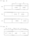
- conditional micro-instruction has such a format as shown in Fig. 2 (a), in which COND is the condition field with C-bit length, which indicates the condition to be checked.
- ADRS is the address field with a-bit length, which includes the information related to address control.
- Condition selector 105 selects status signal STATE m among 2 ⁇ C kinds if status signals STATE m (m is 0 to 2 ⁇ C) which are generated within the information processing device.
- Branch control signal generating circuit 106 receives the selected status signal from the selector 105 and the detection signal from the decoder 104 to generate a branch control signal BRANCH if the selected status signal STATE n is true.
- microprogram counter 101 The low order address of microprogram counter 101 is replaced with the content of the address field ADRS of the branch micro-instruction, while the content of the said microprogram counter 101 is ordinarily incremented by one if the selected status signal is not true.
- microprogram counter 101 determines whether the present content of microprogram counter 101 is M. If conditional control signal BRANCH is false the content of the micro-program counter 101 is renewed to M + 1 at the end of the execution of micro-instruction latched in micro-instruction register 103. On the contrary, if the conditional control signal BRANCH is true, the content of the microprogram counter 101 becomes int (M/2 ⁇ a*2 ⁇ a)+x at the end of the execution the said micro-instruction, so that the branch operation is executed.
- One of the performances required for the branch micro-instruction is that the scope of controllable address is sufficiently large to describe the microprogram. In other words, it means that the bit-width a of address field ADRS is large. Also, it is required as the other one of branch micro-instruction's functions that larger number of conditions may be checked. The latter means that the bit-width c of the condition field COND is sufficiently large.
- Figs. 2 (b) and (c) show respectively the format of conditional branch micro-instruction other than conditional branch micro-instruction as described above.
- limitation is imposed upon the number of detectable conditions, because the bulk of program increases.
- detactable condition number is limited up to 2 ⁇ c.
- the condition to be selected be the least requirements, that is, the greatest common divisor for the whole microprogram.
- PSW processor status words
- SF sign flag
- ZF zero flag
- OF overflow flag
- CF carry flag
- the greatest common divisor of conditions to be checked are four kinds of flag conditions such as SF, ZF, OF, and CF. Assumed that all of the above situations are checked by basing upon only conditional branch micro-instruction related to these conditions, it follows that checking itself is impossible but for making use of plural branch micro-instructions according to the kinds of situations, and accordingly that each execution period of condition varies from each other.
- execution of branch micro-instruction frequently courses drop in execution effectivity of microprogram, because, in the case of microprogram control method, execution time is consumed more in executing branch micro-instruction then in doing not branch or sequential program.
- the process branches to PROC-GT if the relation is "greater" and the PROC-NGT if not greater.
- if-sentence describes conditional branch micro-instructions
- goto-sentence describes branch micro-instructions.
- each instruction becomes able to be executed during T cycles where no branch arises. But it is executed during 2T cycles where any branch arises.
- branch micro-instructions In an information processing apparatus by a microprogram control method using a conventional program counter, micro-instructions called branch micro-instructions are used so as to change the sequence of control.
- the branch micro-instruction changes the sequence of control by replacing a portion or all of the present content of the micro-program counter by the content of the branch address field which the branch micro-instruction has as an operand.
- a branch micro-instruction which has a condition field as other operands is called a conditional branch micro-instruction.
- Such a conditional branch micro-instruction executes a branch operation only if the designated condition corresponds to the present states inside the information processing apparatus.
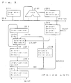
- FIG. 3 shows a block diagram of a conventional microprogram control unit of another type.
- a register file 210 and an arithmetic logical unit 207 are coupled to a data bus 206. Arithmetic and logical operation can be executed with respect to the data stored in the register file 210.
- a microprogrem stored in a micro-instruction memory 201 is accessed by the address designated by an address register 200.
- the above instruction is decoded by an instruction decoder 204 and thereby a micro-instruction is generated with respect to the control point inside the information processing apparatus.
- the micro order MJMP is generated.
- the content of the condition field MOOND of the branch micro-instructions is compared with a status signal STATUS showing the status of the ALU 207. With such a comparison, it is judged whether the branch condition is satisfied, and a branch control signal LDJMP is generated if the condition is satisfied.
- the above address register 200 loads the content of an incrementer 203 which advances the content MA of the address register 200 by one step, and thereby the address content is incremented and the micro-instruction is sequentially accessed.
- an branch operation is executed by loading the output of a branch address generator 209, which generates a branch address designated by the address field of the branch micro-instruction, to the address register 200.
- Such branch operation that changes the branch address according to a single parameter changing on the way of executing the microprogram is called multiway branch function.
- the parameter N can change from 0 to n, and where the procedure 0 which is an assembly of micro-instructions is executed if the parameter N is 0, the procedure 1 is executed if N is 1 and similarly the procedure n is executed if N is n.
- the following plurality of micro-instructions need to be executed so as to realize the above multiway branch function.
- the ALU 207 is used in the steps (1), (3) and (5) because the substraction operation has to be done.
- steps (2), (4) and (6) a conditional branch micro-instruction with condition is used so as to judge whether the result of the calculation by ALU 207 is zero.
- operation micro-instructions as many as at least procedures, and conditional branch micro instructions are used in order to change the procedure to be executed according to the value of the parameter.
- capacity of the microprogram is increased and the mean time necessary to branch to each procedure is increased.
- the execution function of the procedure is designated as a command or status.
- the example such as sign processing in the arithmetical operation of binary coded decimal (BCD) numbers.
- Binary coded decimal (BCD) notation is a kind of numerical value notation system where the decimal numbers 0 to 9 are converted to the binary numbers with four bits 0000 to 1001. Each four bits is called digit, and two digits of BCD are stored in one byte (8 bits). Such a packed BCD can be discriminated from such an unpacked BCD that one digit of BCD is stored in each one byte data.
- Fig. 4 shows a general format of the unpacked BCD.
- the upper digit of the bite data Bn(in case the length of digit which expresses a numerical value is odd) including the most significant digit (MSD) or of the subsequent byte data Bn + 1 (in case that the length of digit which expresses a numerical value is even) to the byte data Bn including the MSD, designates whether the expressed decimal nember is positive or negative by means of the digit which expresses each numerical value as the sign digit.
- the digits excluding the sign digit are called numerical digits.
- a sign digit expresses the sign of a decimal number according to the value of the sign digit. The value used most frequently are, however, the incorrect values such as 1010 to 1111. The typical example illustrating the corresponding relationship between the content of the sign digit and the sign thereof is shown hereinafter. sign digit sign 1010 positive 1011 negative 1100 positive 1101 negative 1110 positive 1111 positive
- the sign is positive if the value of the least significant bit (LSB) of the sign digit is 0, and the sign is negative if the value of LSB is 1.
- the sign is exceptionally positive if the sign digit is 1111.
- the sign digit is the value excluding the listed values, such as the values 0000 to 1001 (these values are in the correct region as numerical values, and the correct region and incorrect region excludes each other), it is necessary to detect the error in the expression method as the whole decimal numbers.
- the process is branched respectively into the procedure "proc-plus” dealing with the positive numbers, into the procedure “proc-minus” dealing with the negative numbers and into the procedure "proc-error” executed in case of detecting an error in the expression method according to the content of the sign digital.
- the multiway branch function to execute the above procedures is shown as follows. where SIGN indicates the content of the sign digit.
- the above-mentioned process on the sign digit is the pre-edit which has to be necessarilly executed in case of calculating BCD.
- the execution time for the above process is necessarily reflected in the execution time for BCD operation.
- the execution time for processing the sign digit is a dominant factor in improvig the capacity.
- the values 0000 to 1001 are correct and the values 1010 to 1111 are incorrect and to be detected as errors.
- the numerical digit is stored being divided into upper four bits and lower four bits of each byte data. In checking the justification of each digit, it is thus necessary to adjust the digit of LSB position according to whether the digit is in the even position or in the odd position.
- Another object of the present invention is to provide a microprogram control unit which can be operated at a high speed.
- a further object of the present invention to provide a program control unit with which a plurality of the states can be checked by the only one conditional branch micro-instruction.
- a further object of the present invention is to provide a micro-instruction control unit which can rapidly carry out a branch operation with a short length of instruction.
- a still another object of the present invention is to provide such a micro-instruction control circuit which can execute a multiway branch with an instruction of a short word length and at a high speed.
- a microprogram control unit for processing conditional branch micro-instructions stored in a micro-instruction memory to control the function of an information processing apparatus, which comprising: a microprogram counter coupled to the micro-instruction memory and containing address for accessing the micro-instruction stored in the memory; means for registering the micro-instruction received from the micro-instruction memory and having an address field coupled to the microprogram counter and a condition field for designating a condition to be judged; detecting means coupled to the registering means to receive the micro-instruction therefrom and for detecting the conditional branch micro-instruction; means for generating status signals representing respectively a plurality of the status of the information processing apparatus and selectively outputting anyone of the status signals; and means for judging the coincidence between the status signal selectively outputted from the status signal generating means and the condition designated by the content of the condition field of the micro-instruction registered by the registering means to output a
- a microprogram control unit which includes a micro-instruction address register, comprising first means for latching at least a portion of a data, second means for extracting a portion of the data latched in the first means, third means for selectively masking a portion of the data extracted by the second means and replacing a portion of the content of the address register by the partially mask data.
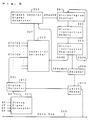
- Fig. 5 shows a block diagram of the microprogram control unit according to an embodiment of the present invention.
- the microprogram control unit includes a microprogram counter 301 which contains the address information for accessing the micro-instruction to be executed and which, after the execution of the non-branched instruction, normally increments one memory address at a time for obtaining the program sequence from sequential memory locations.
- the microprogram counter 301 is coupled to a micro-instruction memory or multiplexer 302 from which the micro-instruction having an address corresponding to the content of the microprogram counter 301 is outputted.
- the microprogram control unit further includes a register 303 for latching the outputted micro-instructions, and a decoder 304 for decoding the micro-instruction outputted from the register 303.
- the micro-instruction is composed of a condition field and an address field.
- the content of the address field of the micro-instruction latched in the micro-instruction register 303 is outputted to the microprogram counter 301 for resetting the address field thereby in accordance with a branch control signal BRANCH.
- the microprogram control unit For generating the branch control signal BRANCH, the microprogram control unit includes a circuit 311 for generating the status signal.
- the circuit 311 may be coupled, for example, to an arithmetic and logic unit which is not shown in Fig. 5 for simplifying the drawing and clearly representing the characteristics of the present invention.
- flag signals SF, ZF, CF and OF are inputted to the status signal generating circuit 311.
- the status signal generating circuit 311 generates, from these four signals, status signals G0 to G15 in accordance with the logic shown in Table 1. These status signals G0 to G15 designates respectively the status of the information processing apparatus after the execution of subtraction of two binary numbers.
- the microprogram control unit further includes a latch means 310 which receives a signal STROBE from the micro-instruction decoder 304 when the decoder 304 detects a conditional branch micro-instruction, and is coupled to a data bus 300.
- the latch means 310 latches a transfer instruction from the data bus 300 in accordance with the signal STROBE to output a selection signal to a status selector 312.
- the latch means 310 latches the lower four bits of the data present on the data bus 300.
- a status selector 312 which is composed of a multiplexer, is coupled with the status signal generating circuit 311 for receiving the status signals Gn therefrom and selects a status signal in accordance with the selection signal outputted from the latch means 310.
- the selecting operation by the status selector 312 is illustrated in Table II.
- the status selector 312 selectively outputs a selected status signal SEL to a condition selector 305 which receives also the content COND m in the condition field of the micro-instruction outputted from the register 303.
- the condition selector 305 compares the selected status signal SEL with the content COND m of the condition field of the micro-instruction.
- the microprogram control unit further includes a circuit 306 for generating a branch control signal BRANCH.
- the branch control signal generating circuit 306 receives a detection signal C BRANCH from the decoder 304 and the condition signal from the condition selector 305 so as to generate the branch control signal BRANCH.
- the branch control signal generating circuit 306 outputs the branch control signal BRANCH to the microprogram counter 301 when the condition signal is true.
- the microprogram counter 301 receives also the content ADRS of the address field of the micro-instruction from the micro-instruction register 303 when the branch control signal is active. Thus, the microprogram counter 301 replaces it's address field with the address signal ADRS in accordance with the branch control signal BRANCH.
- the transfer micro-instruction orders that the latch means 310 latches a transfer signal (1100b) from the data bus 300.
- the status selector 312 receives and decodes the transfer signal (1100b) from the latch means 310.
- the status signal generating circuit 311 generates 16 kinds of status signals from the flag signals SF, ZF, CF and OF, as shown in Table III.
- the status selector 312 selects the status signal G1 and outputs the same as a selected status signal SEL to the condition selector 305.
- the status signal G1 is "0" and therefore the selected status signal SEL becomes "0". Accordingly, when the selected status signal SEL is "0", the condition designated by the micro-instruction corresponds to the result of the calculation.
- the condition designated by the micro-instruction does not satisfy the status after the calculation.
- the condition signal COND from the micro-instruction becomes m
- the branch control signal generating circuit 306 does not generate the branch control signal BRANCH, so that the branch operation is not conducted and the microprogram counter 301 increments the content of its address field by "1".
- the microprogram counter 301 outputs the next address signal (M + 1) to access to the portion of the memory 302 where the next conditional branch micro-instruction is stored.
- a transfer micro-instruction 5 (0101b) is ordered so that it is latched by the latch means 310 from the data bus 300.
- the status signal G5 which indicates that A is not equal to B, is "1".
- the selected status signal SEL becomes "1".
- condition field COND of the conditional branch micro-instruction becomes m
- FIG. 6 is a block diagram of an example where a conditional branch instruction, which is visible to the user, (which will be referred to "macro-instruction" in order to distinguish the same from the micro-instruction) is processed.
- a communication register 402 to which a decoder unit 401 and an execution unit 403 are coupled, so that communication may be conducted between the units 401 and 403.
- the communication register 402 receives the decoded information from the decoder unit 401 and transfers the same to the execution unit 403 for executing the microprogram therein.
- the macro-instruction has an instruction format as shown in Fig. 7. That is, the macro-instruction is composed of the most significant byte or the first byte consisting of an operand OP and a condition field CON, the second and the third bytes containing respectively the lower and higher codes of the branch address designated by the macro-instruction.
- the communication register 402 latches the decoded content z of the condition field CON (four bits) of the conditional branch macro-instruction.
- the relation between the selection signal inputted to the status selector 312 (that is, the output signal of the status selecting latch means 310) and the status signals G0 to G15 is adjusted to correspond to the condition field of the conditional branch macro-instruction. Accordingly, it is not necessary to prepare a microprogram for each conditional branch macro-instruction. Thus, all of the conditional branch macro-instructions can be treated by only one microprogram.
- conditional branch macro-instruction is treated in the execution unit 403 as follows:
- the steps (2) and (3) are executed for each condition designated by the macro-instruction.
- only one microprogram is necessary regardless of the number of conditions (in the present example, the number of conditions is 16).
- FIG. 8 another embodiment of the present invention will be explained, wherein the status signal generating circuit 311 and the status selector 312 shown in Fig. 5 are united to a circuit 311a for generating a selected status signal.
- the latch means 310 for registering the transfer instruction is coupled directly to the circuit 311a for generating the selected status signal SEL.
- the circuit 311a generates the signal SEL according to the logic as shown in Table IV.
- the combination logic shown in Table IV is a logical sum of 18 items of logical multiplies.
- a circuit for such a combination logic may be obtained by means of programmable logic array (PLA) which has been well known in the art.
- PLA programmable logic array
- FIG. 9 there is shown another embodiment of the microprogram control unit in accordance with the present invention.
- the microprogram control unit of the present embodiment is to improve the one of the prior art which has been explained with reference to Fig. 3, and is for processing multibranch micro-instructions.
- the shown unit includes an address register 503 adopted to latch the address for accessing a microinstruction to be executed at the next time in the case that the microprograms are executed in the sequence generated by the incrementer 203. Further, in response to the signal LDJMP the address register 503 latches the address of the branch target generated by the branch address generator 209 when an unconditional or conditional branch micro-instruction is executed. Also, in response to the signal LDJMP the register 503 latches the address of the branch target generated by a multiway branch address generator 502 when a multi-branch micro-instruction is executed.
- the shown unit includes a multiway branch register 500 coupled to the data bus 206 so as to latch the whole or a portion of the content on the data bus 206 when the latch signal WRMBR is generated.
- the branch register 500 is coupled to a multiplexer 501 which operates to selectively output the content MBR of the multiway branch register 500 in accordance with the value of the selection field "SEL" of the multibranch micro-instruction.
- the output of the multiplexer 501 is inputted to the multiway branch address generator 502 together with the mask field MASK and the base field BASE of the multibranch micro-instruction.
- the generator 502 operates to output the address of the branch target determined by the above three inputs.
- An instruction decoder 504 receives the micro-instruction MD and generates microorders such as the signal WRMBR indicating that the transfer micro-instruction designates the transfer to the multiway branch register 500, and the signal LDMBR showing that the multibranch micro-instruction is executed.
- Fig. 10 illustrates one example of the multibranch instruction, which comprises an operation field OP including the operation code of the multibranch micro-instruction.
- the shown instruction also has a selection field "SEL" for selecting the data to be coupled to the multiway branch address generator 502, from the content of the multiway branch register 500.
- a mask field MASK of the multibranch instruction designates the validity of the bit correspondence to the field of the multiway branch register 500 selected by the selection field SEL, and a field BASE indicates the base address of the branch address.
- the data "params" composed of M b-bit parameters Nm is latched in the multiway branch register 500 in response to the latch signal WRMBR generated by the instruction decoder 504 when the transfer micro-instruction is executed.
- the instruction decoder 504 When the multibranch micro-instruction is latched in the instruction latch 202 (Fig. 3), the instruction decoder 504 generates the microorder LDMBR.
- the memory 201 (Fig. 3) outputs the parameter Nsel designated by the selection field SEL of the multibranch micro-instruction.
- the multiway branch address generator 502 derives the logical product of the parameter Nsel and the mask field MASK, and combines n "O"s to the result of product so as to generate a less significant [b + z bits] of the branch address.
- the multibranch micro-instruction detection signal LOMBR is generated, the output of the address generator 502 is latched in the (b + z) less significant bits of the address register 503, and the base field BASE of the multibranch micro-instruction is latched in more significant bit portion of the register 503, so that the address of a new branch target is generated in the register 503.
- new-adrs base*(2 ⁇ (b+z))-params (sel) and mask)*(s ⁇ z) ; where "new-adrs" is the address of branch target "Params(sel)" is the b-bit data of the multiway branch register 500 selected by the selection field SEL.
- FIG. 12 there is shown the structure of the device in accordance with the present invention in more detailed form.
- a 8-bit register 600 is coupled to the data bus 206, and the 8-bit parameter latched in the register 600 is halved, so that a first 4 bit data and a second 4 bit data are connected to a multiplexer 601.
- the multiplexer 601 selects one of the two 4-bit data from the multiplexer 601 in accordance with the selection field SEL. Therefore, it is possible to branch in sixteen ways at maximum.
- the multibranch micro-instruction has the format of 13 bits, as shown in Fig. 13.
- the micro-instruction includes a 4-bit operation code field OP, a 3-bit base address field BASE, a 1-bit selection field SEL, a 4-bit mask field MASK and a 1-bit field DLY which does not concern the present invention.
- the multibranch micro-instruction is expressed as follows: MJMPO (adrs, mask); MJMPI (adrs, mask); Both these micro-instructions are common to each other, excepting that the MJMPO puts "0" in the selection field SEL and the MJMPl puts "1" in the selection field SEL.
- MJMPO adrs, mask
- MJMPI adrs, mask
- Both these micro-instructions are common to each other, excepting that the MJMPO puts "0" in the selection field SEL and the MJMPl puts "1" in the selection field SEL.
- the micro-instruction memory 201 (Fig. 3) includes a 16-bit address space for storing the address MAO-15 of the micro-instruction which should be executed at the next time by an address register 604.
- the 4-bit output of the multiplexer 601 is connected through an array of two-input AND gates 610-613 to the address register 604.
- Each of the AND gates is connected at its one end to each bit output of the multiplexer 601, and at its other end to receive a corresponding bit of the field MASK.
- the address register 604 latches at its more significant 8 bits the more significant 8 bits of the multibranch micro-instruction. Further, the address register 604 latches at its succeeding less significant 3 bits the base address field BASE of the multibranch micro-instruction, and at its further less significant 4 bits the output of the four AND gates 603. In addition, one bit of logic value "0" is latched to the least significant bit of the register 604.
- the 8-bit register 600 is coupled to the least significant 8 bits of the data bus 206, and latches the 8-bits of the data bus 206 when the latch signal WRMBR is rendered active.
- the 4-bit multiplexer 601 operates to selectively output the least significant 4 bits of the 8-bit register 600 when the selection field SEL of the multibranch micro-instruction is "0". On the other hand, when the selection field SEL is "1", the multiplexer 601 outputs the most significant 4 bits of the register 600.
- the output of the 4-bit multiplexer 601 and the mask field MASK of the multibranch micro-instruction are inputted to the array of two-input AND gates 603, and the logical product of 4 bits is latched to intermediate significant 4 bits of the address register 604.
- the address register 604 is set with "00000000100110110b" i.e., the address number 0136.
- the following addresses that is, the execution results of the multibranch micro-instruction MJPI (proc-base, 1111b) can be obtained according to the value of the most significant 4 bit data "n" in the 8-bit register.
- the control is shifted to one of those procedures.
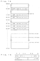
- Fig. 14 illustrates the relationship between such procedures and the location of the micro-instruction.
- procedure process address proc-plus positive numbers 0134, 0138, 0130, 013E proc-minus negative numbers 0136, 013A proc-error errors 0120, 0122, 0124, 0126 0128, 012A 012C, 012E, 0130, 0132
- the control is shifted to "proc-plus” through the address 013C so that the procedure for processing the positive numbers can be started. If the data "0010b" is set, the procedure for executing the error processing can be started since the control is shifted to "proc-error" through the address 0128.
- the value of the 8-bit status is to be set up in the 8-bit register 700, as shown in Fig. 15, by executing a transfer micro-instruction.
- Each bit in the status register 700 is divided into the three fields such as ST0 (3 bits), ST1 (2 bits) and ST2 (1 bit) and located at the bit 0 to 2, bit 5 and 6, and bit 7 in the status register, respectively.
- the bits 3 and 4 in the status register 400 are not defined and are unfixed.
- control can be shifted, for example, to address number 4 if the content of ST1 is 00b, to the address number 8 if the content is 01b, to the address number 0C if the content is 10b and to the address number 0E if the content is the address 11b (base address adrs 1 is added respectively).
- the present invention can provide multibranch micro-instructions with high multiplicity being composed of short micro-instructions. After elongating the length of the multiway branch register 600 and the length of the field SEL for selecting the parameter of the multiway branch micro-instruction, such shorter micro-instructions are obtained by multi-dividing the longer parameter.
- the present invention provides micro-instructions which are very comprehensive, short in the instruction word length and can execute the rapid branch operation without reference to the length and value of the parameter.
Landscapes
- Engineering & Computer Science (AREA)
- Software Systems (AREA)
- Theoretical Computer Science (AREA)
- Physics & Mathematics (AREA)
- General Engineering & Computer Science (AREA)
- General Physics & Mathematics (AREA)
- Executing Machine-Instructions (AREA)
Applications Claiming Priority (7)
| Application Number | Priority Date | Filing Date | Title |
|---|---|---|---|
| JP25005585 | 1985-11-08 | ||
| JP250059/85 | 1985-11-08 | ||
| JP60250059A JP2587407B2 (ja) | 1985-11-08 | 1985-11-08 | マイクロプログラム制御装置 |
| JP250055/85 | 1985-11-08 | ||
| JP25005985 | 1985-11-08 | ||
| JP25005585A JPS62109133A (ja) | 1985-11-08 | 1985-11-08 | マイクロプログラム制御装置 |
| EP86115571A EP0221577B1 (fr) | 1985-11-08 | 1986-11-10 | Unité de commande de microprogramme |
Related Parent Applications (2)
| Application Number | Title | Priority Date | Filing Date |
|---|---|---|---|
| EP86115571.1 Division | 1986-11-10 | ||
| EP86115571A Division EP0221577B1 (fr) | 1985-11-08 | 1986-11-10 | Unité de commande de microprogramme |
Publications (3)
| Publication Number | Publication Date |
|---|---|
| EP0500151A2 true EP0500151A2 (fr) | 1992-08-26 |
| EP0500151A3 EP0500151A3 (en) | 1993-01-13 |
| EP0500151B1 EP0500151B1 (fr) | 2000-03-01 |
Family
ID=26539622
Family Applications (2)
| Application Number | Title | Priority Date | Filing Date |
|---|---|---|---|
| EP86115571A Expired - Lifetime EP0221577B1 (fr) | 1985-11-08 | 1986-11-10 | Unité de commande de microprogramme |
| EP92108451A Expired - Lifetime EP0500151B1 (fr) | 1985-11-08 | 1986-11-10 | Unité de commande de microprogramme |
Family Applications Before (1)
| Application Number | Title | Priority Date | Filing Date |
|---|---|---|---|
| EP86115571A Expired - Lifetime EP0221577B1 (fr) | 1985-11-08 | 1986-11-10 | Unité de commande de microprogramme |
Country Status (3)
| Country | Link |
|---|---|
| US (1) | US4907192A (fr) |
| EP (2) | EP0221577B1 (fr) |
| DE (2) | DE3650740D1 (fr) |
Cited By (4)
| Publication number | Priority date | Publication date | Assignee | Title |
|---|---|---|---|---|
| EP0649083A3 (fr) * | 1993-10-18 | 1995-05-10 | Cyrix Corp | |
| US5644741A (en) * | 1993-10-18 | 1997-07-01 | Cyrix Corporation | Processor with single clock decode architecture employing single microROM |
| US5794026A (en) * | 1993-10-18 | 1998-08-11 | National Semiconductor | Microprocessor having expedited execution of condition dependent instructions |
| SG95605A1 (en) * | 1998-10-13 | 2003-04-23 | Motorola Inc | Data processor system and instruction system using grouping |
Families Citing this family (25)
| Publication number | Priority date | Publication date | Assignee | Title |
|---|---|---|---|---|
| JP2723238B2 (ja) * | 1988-01-18 | 1998-03-09 | 株式会社東芝 | 情報処理装置 |
| CA1311063C (fr) * | 1988-12-16 | 1992-12-01 | Tokumichi Murakami | Processeur de signaux numeriques |
| JPH031231A (ja) * | 1989-02-09 | 1991-01-07 | Nec Corp | マイクロプログラム制御装置 |
| JP2511151B2 (ja) * | 1989-09-11 | 1996-06-26 | 富士通株式会社 | デ―タ処理装置 |
| CA2030404A1 (fr) * | 1989-11-27 | 1991-05-28 | Robert W. Horst | Sequenceur de macroinstructions |
| JPH03288228A (ja) * | 1990-04-04 | 1991-12-18 | Koufu Nippon Denki Kk | 情報処理装置 |
| US5371862A (en) * | 1991-02-27 | 1994-12-06 | Kabushiki Kaisha Toshiba | Program execution control system |
| US5410660A (en) * | 1992-12-24 | 1995-04-25 | Motorola, Inc. | System and method for executing branch on bit set/clear instructions using microprogramming flow |
| AU3437293A (en) * | 1993-01-06 | 1994-08-15 | 3Do Company, The | Digital signal processor architecture |
| US5471597A (en) * | 1993-12-23 | 1995-11-28 | Unisys Corporation | System and method for executing branch instructions wherein branch target addresses are dynamically selectable under programmer control from writable branch address tables |
| US5815697A (en) * | 1997-01-09 | 1998-09-29 | Texas Instruments Incorporated | Circuits, systems, and methods for reducing microprogram memory power for multiway branching |
| US5872965A (en) * | 1997-06-30 | 1999-02-16 | Sun Microsystems, Inc. | System and method for performing multiway branches using a visual instruction set |
| GB2355084B (en) * | 1999-07-21 | 2004-04-28 | Element 14 Ltd | Setting condition values in a computer |
| US6988189B1 (en) * | 2000-10-31 | 2006-01-17 | Altera Corporation | Ternary content addressable memory based multi-dimensional multi-way branch selector and method of operating same |
| US6851046B1 (en) | 2000-11-14 | 2005-02-01 | Globespanvirata, Inc. | Jumping to a recombine target address which is encoded in a ternary branch instruction |
| US6857063B2 (en) | 2001-02-09 | 2005-02-15 | Freescale Semiconductor, Inc. | Data processor and method of operation |
| US7140003B2 (en) * | 2003-02-14 | 2006-11-21 | International Business Machines Corporation | Method and system for specifying sets of instructions for selection by an instruction generator |
| US8342524B2 (en) | 2003-08-27 | 2013-01-01 | Winsor Corporation | Virtual game |
| US8074985B2 (en) * | 2003-08-27 | 2011-12-13 | Winsor Concepts | Virtual game |
| US7216218B2 (en) * | 2004-06-02 | 2007-05-08 | Broadcom Corporation | Microprocessor with high speed memory integrated in load/store unit to efficiently perform scatter and gather operations |
| US7747843B2 (en) * | 2004-06-02 | 2010-06-29 | Broadcom Corporation | Microprocessor with integrated high speed memory |
| US7383547B1 (en) * | 2004-12-03 | 2008-06-03 | Lecroy Corporation | Apparatus and technique for device emulation |
| JP4038216B2 (ja) * | 2005-05-10 | 2008-01-23 | ファナック株式会社 | シーケンスプログラム編集装置 |
| US20090249047A1 (en) * | 2008-03-31 | 2009-10-01 | International Business Machines Corporation | Method and system for relative multiple-target branch instruction execution in a processor |
| US10092824B2 (en) | 2010-09-30 | 2018-10-09 | Winsor Concepts | Entertainment apparatus and method |
Family Cites Families (13)
| Publication number | Priority date | Publication date | Assignee | Title |
|---|---|---|---|---|
| JPS52116131A (en) * | 1976-03-26 | 1977-09-29 | Toshiba Corp | Microprogram instruction control unit |
| DE2622974A1 (de) * | 1976-05-21 | 1977-11-24 | Siemens Ag | Mikroprogrammierbares steuerwerk |
| SU615538A1 (ru) * | 1976-07-07 | 1978-07-15 | Предприятие П/Я В-2892 | Устройство дл выбора информации из блока пам ти |
| FR2359461A1 (fr) * | 1976-07-23 | 1978-02-17 | Thomson Csf | Unite de controle microprogrammable et circuit d'interface comportant une telle unite de controle |
| IT1123613B (it) * | 1976-10-07 | 1986-04-30 | Sits Soc It Telecom Siemens | Unita' di controllo a microprogrammi per elaboratori di dati |
| US4323964A (en) * | 1976-11-01 | 1982-04-06 | Data General Corporation | CPU Employing micro programmable control for use in a data processing system |
| US4179737A (en) * | 1977-12-23 | 1979-12-18 | Burroughs Corporation | Means and methods for providing greater speed and flexibility of microinstruction sequencing |
| US4338661A (en) * | 1979-05-21 | 1982-07-06 | Motorola, Inc. | Conditional branch unit for microprogrammed data processor |
| US4430711A (en) * | 1980-05-30 | 1984-02-07 | Signetics Corporation | Central processing unit |
| US4373180A (en) * | 1980-07-09 | 1983-02-08 | Sperry Corporation | Microprogrammed control system capable of pipelining even when executing a conditional branch instruction |
| IT1134780B (it) * | 1980-12-18 | 1986-08-13 | Honeywell Inf Systems | Unita' di controllo microprogrammata con rete di salti multipli |
| US4472772A (en) * | 1981-08-03 | 1984-09-18 | Burroughs Corporation | High speed microinstruction execution apparatus |
| US4754393A (en) * | 1984-12-21 | 1988-06-28 | Advanced Micro Devices, Inc. | Single-chip programmable controller |
-
1986
- 1986-11-10 EP EP86115571A patent/EP0221577B1/fr not_active Expired - Lifetime
- 1986-11-10 DE DE3650740T patent/DE3650740D1/de not_active Expired - Fee Related
- 1986-11-10 EP EP92108451A patent/EP0500151B1/fr not_active Expired - Lifetime
- 1986-11-10 US US06/928,421 patent/US4907192A/en not_active Expired - Lifetime
- 1986-11-10 DE DE3650473T patent/DE3650473T2/de not_active Expired - Fee Related
Cited By (4)
| Publication number | Priority date | Publication date | Assignee | Title |
|---|---|---|---|---|
| EP0649083A3 (fr) * | 1993-10-18 | 1995-05-10 | Cyrix Corp | |
| US5644741A (en) * | 1993-10-18 | 1997-07-01 | Cyrix Corporation | Processor with single clock decode architecture employing single microROM |
| US5794026A (en) * | 1993-10-18 | 1998-08-11 | National Semiconductor | Microprocessor having expedited execution of condition dependent instructions |
| SG95605A1 (en) * | 1998-10-13 | 2003-04-23 | Motorola Inc | Data processor system and instruction system using grouping |
Also Published As
| Publication number | Publication date |
|---|---|
| EP0500151B1 (fr) | 2000-03-01 |
| EP0221577B1 (fr) | 1996-01-17 |
| DE3650740D1 (de) | 2000-04-06 |
| EP0221577A2 (fr) | 1987-05-13 |
| DE3650473T2 (de) | 1996-08-14 |
| US4907192A (en) | 1990-03-06 |
| EP0500151A3 (en) | 1993-01-13 |
| EP0221577A3 (en) | 1989-02-01 |
| DE3650473D1 (de) | 1996-02-29 |
Similar Documents
| Publication | Publication Date | Title |
|---|---|---|
| EP0500151A2 (fr) | Unité de commande de microprogramme | |
| US6205534B1 (en) | Apparatus and method for processing data with a plurality of flag groups | |
| US5241492A (en) | Apparatus for performing multiply and accumulate instructions with reduced power and a method therefor | |
| US5128890A (en) | Apparatus for performing multiplications with reduced power and a method therefor | |
| US5210833A (en) | System for selectively masking data in a branch address register and replacing the microinstruction address register by the masked data | |
| US4001788A (en) | Pathfinder microprogram control system | |
| JPS60151761A (ja) | 10進演算用に連続したデ−タ装置をアクセスするためのニブルおよびワ−ド・アドレス指定可能なメモリ− | |
| US6036350A (en) | Method of sorting signed numbers and solving absolute differences using packed instructions | |
| JPH06202850A (ja) | データ処理装置 | |
| JPH0145649B2 (fr) | ||
| US4484300A (en) | Data processor having units carry and tens carry apparatus supporting a decimal multiply operation | |
| US6499046B1 (en) | Saturation detection apparatus and method therefor | |
| US5185870A (en) | System to determine if modification of first macroinstruction to execute in fewer clock cycles | |
| US5265204A (en) | Method and apparatus for bit operational process | |
| US4942547A (en) | Multiprocessors on a single semiconductor chip | |
| US4245328A (en) | Binary coded decimal correction apparatus for use in an arithmetic unit of a data processing unit | |
| EP0936537B1 (fr) | Contrôle de redondance cyclique dans un système informatique | |
| JPS5838819B2 (ja) | デ−タ処理システム用制御ファイル装置 | |
| US5034900A (en) | Method and apparatus for bit operational process | |
| US5519881A (en) | Priority encoder for accessing multiple registers simultaneously and a data processing system which uses it | |
| EP0168406B1 (fr) | Generateur de codes de condition de virgule flottante | |
| EP0343668B1 (fr) | Système de commande de normalisation pour des opérations arithmétiques à virgule flottante | |
| EP0141752B1 (fr) | Système de commande à micro-code pour un système de traitement de données | |
| US5968165A (en) | System and method for minimizing the size of operands | |
| EP0153025B1 (fr) | Commande à microprogramme |
Legal Events
| Date | Code | Title | Description |
|---|---|---|---|
| PUAI | Public reference made under article 153(3) epc to a published international application that has entered the european phase |
Free format text: ORIGINAL CODE: 0009012 |
|
| AC | Divisional application: reference to earlier application |
Ref document number: 221577 Country of ref document: EP |
|
| AK | Designated contracting states |
Kind code of ref document: A2 Designated state(s): DE FR GB |
|
| PUAL | Search report despatched |
Free format text: ORIGINAL CODE: 0009013 |
|
| AK | Designated contracting states |
Kind code of ref document: A3 Designated state(s): DE FR GB |
|
| 17P | Request for examination filed |
Effective date: 19921228 |
|
| 17Q | First examination report despatched |
Effective date: 19961203 |
|
| GRAG | Despatch of communication of intention to grant |
Free format text: ORIGINAL CODE: EPIDOS AGRA |
|
| GRAG | Despatch of communication of intention to grant |
Free format text: ORIGINAL CODE: EPIDOS AGRA |
|
| GRAH | Despatch of communication of intention to grant a patent |
Free format text: ORIGINAL CODE: EPIDOS IGRA |
|
| GRAH | Despatch of communication of intention to grant a patent |
Free format text: ORIGINAL CODE: EPIDOS IGRA |
|
| GRAA | (expected) grant |
Free format text: ORIGINAL CODE: 0009210 |
|
| AC | Divisional application: reference to earlier application |
Ref document number: 221577 Country of ref document: EP |
|
| AK | Designated contracting states |
Kind code of ref document: B1 Designated state(s): DE FR GB |
|
| REF | Corresponds to: |
Ref document number: 3650740 Country of ref document: DE Date of ref document: 20000406 |
|
| ET | Fr: translation filed | ||
| PLBE | No opposition filed within time limit |
Free format text: ORIGINAL CODE: 0009261 |
|
| STAA | Information on the status of an ep patent application or granted ep patent |
Free format text: STATUS: NO OPPOSITION FILED WITHIN TIME LIMIT |
|
| 26N | No opposition filed | ||
| REG | Reference to a national code |
Ref country code: GB Ref legal event code: IF02 |
|
| REG | Reference to a national code |
Ref country code: GB Ref legal event code: 732E |
|
| REG | Reference to a national code |
Ref country code: FR Ref legal event code: TP |
|
| PGFP | Annual fee paid to national office [announced via postgrant information from national office to epo] |
Ref country code: GB Payment date: 20031105 Year of fee payment: 18 |
|
| PGFP | Annual fee paid to national office [announced via postgrant information from national office to epo] |
Ref country code: FR Payment date: 20031110 Year of fee payment: 18 |
|
| PGFP | Annual fee paid to national office [announced via postgrant information from national office to epo] |
Ref country code: DE Payment date: 20031120 Year of fee payment: 18 |
|
| PG25 | Lapsed in a contracting state [announced via postgrant information from national office to epo] |
Ref country code: GB Free format text: LAPSE BECAUSE OF NON-PAYMENT OF DUE FEES Effective date: 20041110 |
|
| PG25 | Lapsed in a contracting state [announced via postgrant information from national office to epo] |
Ref country code: DE Free format text: LAPSE BECAUSE OF NON-PAYMENT OF DUE FEES Effective date: 20050601 |
|
| GBPC | Gb: european patent ceased through non-payment of renewal fee |
Effective date: 20041110 |
|
| PG25 | Lapsed in a contracting state [announced via postgrant information from national office to epo] |
Ref country code: FR Free format text: LAPSE BECAUSE OF NON-PAYMENT OF DUE FEES Effective date: 20050729 |
|
| REG | Reference to a national code |
Ref country code: FR Ref legal event code: ST |