EP0500933B1 - Systeme de transmission/reception de signaux video - Google Patents
Systeme de transmission/reception de signaux video Download PDFInfo
- Publication number
- EP0500933B1 EP0500933B1 EP90913550A EP90913550A EP0500933B1 EP 0500933 B1 EP0500933 B1 EP 0500933B1 EP 90913550 A EP90913550 A EP 90913550A EP 90913550 A EP90913550 A EP 90913550A EP 0500933 B1 EP0500933 B1 EP 0500933B1
- Authority
- EP
- European Patent Office
- Prior art keywords
- video signal
- signal
- motion
- circuit
- pass filter
- Prior art date
- Legal status (The legal status is an assumption and is not a legal conclusion. Google has not performed a legal analysis and makes no representation as to the accuracy of the status listed.)
- Expired - Lifetime
Links
Images




Classifications
-
- H—ELECTRICITY
- H04—ELECTRIC COMMUNICATION TECHNIQUE
- H04N—PICTORIAL COMMUNICATION, e.g. TELEVISION
- H04N7/00—Television systems
- H04N7/01—Conversion of standards, e.g. involving analogue television standards or digital television standards processed at pixel level
- H04N7/0117—Conversion of standards, e.g. involving analogue television standards or digital television standards processed at pixel level involving conversion of the spatial resolution of the incoming video signal
- H04N7/012—Conversion between an interlaced and a progressive signal
-
- H—ELECTRICITY
- H04—ELECTRIC COMMUNICATION TECHNIQUE
- H04N—PICTORIAL COMMUNICATION, e.g. TELEVISION
- H04N5/00—Details of television systems
- H04N5/14—Picture signal circuitry for video frequency region
- H04N5/144—Movement detection
Definitions
- the present invention relates to video signal transmission/reception systems.
- a motion detection operation for detecting whether a picture is a still image or real moving image is carried out and then proper signal processing is carried out on the basis of resultant detected motion information.
- a composite video signal for example, is separated into a luminance signal and color difference signals, the separation processing is carried out at respective frequency bands by utilizing only video signals within the same frame if a picture is a real moving image. If a picture is a still image, then video signals of adjacent frames are utilized and the separating processing is carried out by a comb filter, whereby optimum processing is carried out in response to the signal conditions.
- a conventional motion detecting circuit is of low accuracy in detecting motion of a picture.
- motion detection is carried out on a basis of a vertical correlation of pictures between adjacent fields, for example, there is then the disadvantage that a still image is erroneously detected as being a real moving image at a portion in which no vertical correlation is present.
- responsiveness is lowered by widening a motion detection range or a motion is identified by using also motion detection information provided by other methods. If the responsiveness is lowered as described above, there is then the disadvantage that resolution of a processed video signal is lowered. Further, of a plurality of items of motion detection information are obtained, there is then the problem that the arrangement of the motion detecting circuit becomes complex.
- European Patent Application Publication No EP-A-0 082 489 discloses a video signal transmission/reception systems in which an image pick-up unit produces a video signal by line sequential scanning. That signal is then passed to a first spatio-temperal low-pass filter which effects filtering at least vertically and temporally, the passing region being such that the filter removes undesired signal components, namely a sampling frequency component and harmonics thereof, which are generated by the sampling required for scanning conversion. (That is, the filter performs an anti-aliasing function). The signal is then converted to an interlace scanning signal and transmitted. On reception, the signal is passed to a second spatio-temperal low-pass filter similar to the first one.
- Motion of the picture represented by the video signal may be detected from an inter-frame difference signal component and the passing region of the first or second spatio-temperal filter may be adaptively controlled in accordance with the detected motion.
- the motion detection may be effected at the reception side of the system if the transmission side of the system is constructed in a conventional manner (the first filter is not provided) and the second filter is adaptively controlled.
- the present invention seeks to provide a video signal transmission/reception system of a simplified configuration in which motion detection can be carried out reliably on the reception side of the system.
- a video signal transmission/reception system comprising: an image pick-up unit for producing a video signal by sequential scanning; a low-pass filter operative to limit the vertical frequency band of said video signal to a frequency band lower than an upper limit of a transmissible band; a converting circuit for converting the sequential scanning video signal as vertically band-limited by the low-pass filter into an interlace scanning video signal; a transmission circuit for transmitting the interlace scanning video signal; a reception circuit for receiving the transmitted video signal; a high-pass filter for extracting from the received video signal a component signal generated in a predetermined vertical frequency band between the vertical frequency band to which the signal was limited by the low-pass filter and the upper limit of the transmissible band; a motion detection circuit for detecting motion in the received video signal from said extracted component signal; and a signal processing circuit controlled on the basis of said motion detected by the motion detection circuit.
- a motion detection operation of high accuracy can be carried out by a simple arrangement in which the video signal component of the predetermined vertical frequency band is identified only on the reception side.
- FIG. 1 An arrangement of a transmission side of the system is illustrated in FIG 1.
- An image pick-up unit formed by a video camera 1 picks up an image according to the line sequential scanning manner at every field to output as image signals three primary color signals 2R, 2G and 2B of a so-called double scanning based on line sequential scanning of horizontal scanning lines (525 lines per field) at twice the ordinary number of scanning lines per field.
- These image signals 2R, 2G and 2B are supplied to a matrix circuit 2 and converted into a luminance signal 2Y and color difference signals 2(R-Y) and 2(B-Y) for double speed scanning by the matrix circuit 2.
- the luminance signal 2Y and the color difference signals 2(R-Y) and 2(B-Y) thus converted are supplied to low-pass filters 3a, 3b and 3c respectively.
- Each of the low-pass filters 3a, 3b and 3c is adapted to pass a band of a video signal having a frequency less than a predetermined frequency, which will be described later.
- Output signals of these low-pass filters 3a, 3b, 3c are supplied to a scan converting circuit 4, and horizontal scanning lines of one field are converted to a half, i.e., 262.5 to thereby provide a luminance signal Y and color difference signals R-Y and B-Y conforming to the ordinary broadcast standards for interlace scanning.
- the luminance signal Y and the color difference signals R-Y and B-Y output from the scan converting circuit 4 are supplied to an encoder 5, in which they are converted into a composite video signal according to the NTSC broadcast standards, which then is fed to an output terminal 6.
- the composite video signal developed at the output terminal 6 is processed by some suitable method such as carrier modulation or the like and then transmitted by means of a wireless or wire system.
- these filters are each formed of a transversal filter.
- This transversal filter is disclosed in Japanese Patent Application Publication No. JP-A-60-203013, for example, and constructed as shown in FIG. 2 in this embodiment. More specifically, a signal applied to an input terminal 31 is supplied to a series circuit of memories 32a, 32b, 32c, 32d, each of which is provided as delay means for delaying the above signal by one horizontal scanning period (one horizontal scanning period of a double speed scanning signal). Output signals of the respective memories 32a, 32b, 32c and 32d are supplied through respective coefficient multipliers 33a, 33b, 33c, 33d to an input terminal of an adder 34 and an added output of the adder 34 is supplied to an output terminal 35.
- the luminance signal 2Y and the color difference signals 2(R-Y) and 2(B-Y) are limited in band by utilizing the transversal filters thus arranged.
- a signal having a vertical frequency near 262.5 c/ph (cycle/picture height) is stopped and only a signal in a frequency band (as shown by a solid line in FIG. 5) below this value is allowed to pass.
- the signal of 262.5c/ph is a signal of an upper limit (broken line) that can be transmitted during the horizontal scanning period according to the NTSC system.
- the color difference signals 2(R-Y) and 2(B-Y) are similarly limited in band and only the color difference signals in a frequency band lower than that of the luminance signal and which are below about 100c/ph as shown in FIG. 6 are allowed to pass. Then, from the respective signals band-limited by the low-pass filters 3a, 3b and 3c, a composite video signal in which the band near the vertical frequency of 262.5c/ph is limited is obtained by the encoder 5 as shown in FIG. 7. In this case, the color subcarrier frequency fsc is 131.25 c/ph.
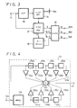
- FIG. 3 The circuitry of the reception side for receiving the video signal transmitted by the above-mentioned arrangement is illustrated in FIG. 3.
- a video signal input terminal 11 is supplied with a composite video signal which results from demodulating the carrier of the received video signal from the transmission side.
- This composite video signal is supplied to a motion adaptive type luminance/chroma separating circuit 12.
- the separating circuit 12 is adapted to separate the composite video signal to provide a luminance signal and a chroma signal and also is adapted to carry out a proper separation processing on the basis of a motion detection information of a picture. More specifically, the video signal applied to an input terminal 11 is supplied to a motion detection high-pass filter 13.
- the high-pass filter 13 is formed by using a transversal filter and is arranged as shown in FIG. 4.
- the composite video signal applied to an input terminal 13a of the high-pass filter 13 is supplied to a series circuit of memories 131a, 131b, 131c and 131d, each of which is provided as delay means for delaying the signal by one horizontal scanning period.
- the input signal to the memory 131a and output signals from the respective memories 131a, 131b, 131c and 131d are supplied through respective coefficient multipliers 132a, 132b, 132c, 132d and 132e to input terminals of an adder 133.
- the composite video signal applied to the input terminal 13a is supplied through a delay circuit 134, which delays the signal by one field period, to a series circuit of memories 135a, 135b and 135c, each of which delays the signal by one scanning period. Then, the output signal of the delay circuit 134 and the output signals from the respective memories 135a, 135b and 135c are supplied through respective coefficient multipliers 136a, 136b, 136c and 136d to input terminals of the adder 133. In this case, only a desired high band signal is extracted by selecting coefficients of the respective coefficient multipliers 132a to 132e and 136a to 136d. Then, the output signal of the adder 133 is supplied to an output terminal 137 as the output signal of the high-pass filter 13.
- the output signal of the high-pass filter 13 thus arranged is utilized as a motion detection signal of a picture.
- a signal of a frequency band extracted from the composite video signal by this high-pass filter 13 is selected to be a signal having a frequency near the vertical frequency of 262.5c/ph as shown in FIG. 8.
- the output signal from the high-pass filter 13 is supplied to a motion detecting circuit 14.
- the motion detecting circuit 14 determines that a picture has a motion, while when the amplitude of the output signal from the filter 13 falls in the thus set range, the motion detecting circuit determines that a picture has no motion. Therefore, the motion detecting circuit supplies control signals corresponding to the respective judged states to the motion adaptive type luminance/chroma separating circuit 12.
- the motion adaptive type luminance/chroma separating circuit 12 When instructed by the control signal that the picture has no motion, the motion adaptive type luminance/chroma separating circuit 12 carries out the separation processing from video signals of adjacent several fields on the basis of a comb filter, while when instructed by the control signal that the picture has a motion, the motion adaptive type luminance/chroma separating circuit carries out the separation processing only from the video signal within one field on the basis of a bandpass filter.
- the luminance signal Y thus separated is supplied to a matrix circuit 15 and the chroma signal C thus separated is supplied to a chroma signal decoder 16.
- the color difference signals R-Y and B-Y are formed from the chroma signal C by the chroma signal decoder 16 and these color difference signals R-Y and B-Y are supplied to the matrix circuit 15.
- Primary color signals R, G and B are obtained from the luminance signal Y and the color difference signals R-Y and B-Y by the matrix circuit 15 and then the respective primary color signals R, G, and B are fed to a picture receiving circuit (not shown) of at a later stage through terminals 16R, 16G and 16B.
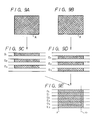
- this received video signal for example, is a still picture. More specifically, let it be assumed that, as shown in FIG. 9A, a rectangular object x is displayed by a picture picked up during a certain odd field and that the object x is displayed at the same position of a picture picked up during the even field (FIG. 9B) next following this odd field. At that time, since the video signal of each field received on the reception side is converted into the interlace scanning video signal, the object x displayed by the video signal of odd field is displayed by lines O1, O2, O3 ...
- FIG. 9E an image of one frame is formed from video signals of respective lines of both fields and an object x′ is displayed in a received image as shown in FIG. 9E.
- a signal is not suddenly changed at every line in a vertical direction H1 near the contour portion of the object x′ while the signal state displaying the object x′ is continued over several lines.
- the motion detecting circuit 14 determines that the picture has no motion.
- the motion detecting circuit 14 supplies a corresponding control signal to the motion adaptive type luminance/chroma separating circuit 12 which then carries out the separation processing by utilizing the comb filter suitable for the still image.
- an image of one frame is formed from the video signals of respective lines of both fields and an object x ⁇ in the received image is displayed.
- the positions of the object x ⁇ displayed by the odd lines O1, O2, O3 ... and the even lines E1, E2, E3 ... are different, whereby a rapid change of signal at every line is presented in a vertical direction H2 near the contour portion of the object x ⁇ . That is, when the video signal at that time is extracted by the reception side high-pass filter 13, the frequency signal component near 262.5 c/ph that appears in the presence of the signal change at every line in the vertical direction is output from the filter 13.
- the motion detecting circuit 14 determines that the picture has a motion.
- the motion detecting circuit 14 supplies a corresponding control signal to the motion adaptive type luminance/chroma separating circuit 12 which then carries out the separating processing by utilizing the bandpass filter suitable for the real moving picture.
- the motion detection is similarly carried out in the case of an object which moves in the vertical direction. That is, let it be assumed that, as shown in FIG. 11A, for example, a rectangular object x is displayed by a picture picked up during a certain odd field and that an object x, which is somewhat moved in the vertical direction, is displayed in a picture picked up during the even field (FIG. 11B) next following the above odd field. At that time, since the video signal of each field received on the reception side is converted into the interlace scanning video signal, the objects x displayed on the odd field and the even field are displayed on the lines O1, O2, O3 ... and E1, E2, E3 ... which are selectively extracted one line each from the image signal as shown in FIGS. 11C and 11D.
- an image of one frame is formed from the video signals of respective lines of both fields and an object x ⁇ ′ in the received image is displayed.
- the object is displayed at every line by only odd line or even line at the position in which the positions of the objects x are not overlapped.
- the displayed portion of the object x ⁇ ′ is seen from a vertical direction H3, then a rapid change of signal at every line occurs.
- the motion detecting circuit 14 determines that the picture has a motion and hence the motion adaptive type luminance/chroma separating circuit 12 carries out the separation processing suitable for a real moving image.
- the vertical frequency is limited on the transmission side and the high band component is extracted from the video signal on the reception side, for thereby carrying out the motion detection of the picture. Therefore, motion detection of high accuracy can be carried out by a simple arrangement.
- the chroma signal color difference signals
- the motion detection of high accuracy can be carried out on the basis of only the luminance component which is free from the influence of the chroma signal. Further, since the motion detection information of high accuracy is obtained as described above, the luminance signal and the chroma signal can always be separated in the optimum condition suitable for the states of picture, which can improve the quality of the received image.
- the motion detection information is utilized for the separation processing of the luminance signal and the chroma signal as described above, it is needless to say that the motion detection information can be utilized in a wide variety of signal processings such as scan speed conversion or the like in order to improve the quality of the received image.
- the present embodiment is applied to the NTSC system as described above, it can be easily understood that the present embodiment is not limited thereto and that it may be applied to other broadcasting systems.
- the present invention is not limited to the above-mentioned embodiment, and various modifications may be effected therein without departing from the scope of the invention.
- motion detection of high accuracy based on the luminance component which is free from the chroma signal, can be effected by a simple arrangement and a satisfactory signal processing based on the motion detection information of high accuracy can be carried out.
Landscapes
- Engineering & Computer Science (AREA)
- Computer Graphics (AREA)
- Multimedia (AREA)
- Signal Processing (AREA)
- Television Systems (AREA)
- Color Television Systems (AREA)
- Processing Of Color Television Signals (AREA)
Abstract
Claims (4)
- Système d'émission et de réception de signaux vidéo, comprenant:- une unité de captage d'images (1) pour produire un signal vidéo par balayage séquentiel;- un filtre passe-bas (3) fonctionnant pour limiter la bande de fréquences verticales dudit signal vidéo à une bande de fréquences inférieure à une limite supérieure d'une bande d'émission;- un circuit convertisseur (4) pour convertir le signal vidéo à balayage séquentiel limité en bande verticalement par le filtre passe-bas en un signal vidéo à balayage entrelacé;- un circuit d'émission pour émettre le signal vidéo à balayage entrelacé;- un circuit de réception pour recevoir le signal vidéo émis;- un filtre passe-haut (13) pour extraire du signal vidéo reçu un signal formant composante produit dans une bande prédéterminée de fréquences verticales entre la bande de fréquences verticales à laquelle le signal a été limité par le filtre passe-bande (3) et la limite supérieure de la bande d'émission;- un circuit de détection de mouvement (14) pour détecter le mouvement dans le signal vidéo reçu à partir dudit signal formant composante extrait; et- un circuit de traitement de signaux (12) commandé sur la base dudit mouvement détecté par ledit circuit de détection de mouvement (14).
- Système d'émission et de réception de signaux vidéo selon la revendication 1, dans lequel ledit balayage séquentiel est un balayage ligne par ligne.
- Système d'émission et de réception de signaux vidéo selon la revendication 1 ou 2, dans lequel ladite bande prédéterminée de fréquences verticales dudit signal formant composante extrait est proche de 525/2 cycles par hauteur d'image.
- Système d'émisson et de réception de signaux vidéo selon la revendication 1, 2 ou 3, dans lequel ledit signal formant composante extrait par le filtre passe-bande (13) est obtenu à partir de deux périodes de trame du signal vidéo reçu.
Applications Claiming Priority (2)
| Application Number | Priority Date | Filing Date | Title |
|---|---|---|---|
| JP1092697A JP2884590B2 (ja) | 1989-04-12 | 1989-04-12 | 映像信号送受信システム、映像信号受信装置及び映像信号送受信方法 |
| PCT/JP1990/001193 WO1992005666A1 (fr) | 1989-04-12 | 1990-09-18 | Systeme de transmission/reception de signaux video |
Publications (3)
| Publication Number | Publication Date |
|---|---|
| EP0500933A1 EP0500933A1 (fr) | 1992-09-02 |
| EP0500933A4 EP0500933A4 (en) | 1993-04-28 |
| EP0500933B1 true EP0500933B1 (fr) | 1995-01-18 |
Family
ID=14061692
Family Applications (1)
| Application Number | Title | Priority Date | Filing Date |
|---|---|---|---|
| EP90913550A Expired - Lifetime EP0500933B1 (fr) | 1989-04-12 | 1990-09-18 | Systeme de transmission/reception de signaux video |
Country Status (5)
| Country | Link |
|---|---|
| US (1) | US5376972A (fr) |
| EP (1) | EP0500933B1 (fr) |
| JP (1) | JP2884590B2 (fr) |
| DE (1) | DE69016216T2 (fr) |
| WO (1) | WO1992005666A1 (fr) |
Families Citing this family (3)
| Publication number | Priority date | Publication date | Assignee | Title |
|---|---|---|---|---|
| EP0605032A1 (fr) * | 1992-12-16 | 1994-07-06 | Laboratoires D'electronique Philips | Etage de détection de mouvement et codeur l'incluant |
| FR2699306A1 (fr) * | 1992-12-16 | 1994-06-17 | Philips Electronique Lab | Etage de détection de mouvement dans des signaux représentatifs d'images à trames entrelacées. |
| US6077816A (en) * | 1995-08-07 | 2000-06-20 | Unilever Home & Personal Care Usa, Division Of Conopco, Inc. | Liquid cleansing composition comprising soluble, lamellar phase inducing structurant |
Family Cites Families (25)
| Publication number | Priority date | Publication date | Assignee | Title |
|---|---|---|---|---|
| US3845498A (en) * | 1973-05-25 | 1974-10-29 | Westinghouse Electric Corp | Receiver for an educational branching system |
| US4551753A (en) * | 1981-12-17 | 1985-11-05 | Nippon Hoso Kyokai | Picture signal processing system including spatio-temporal filter |
| JPS58205377A (ja) * | 1982-05-26 | 1983-11-30 | Nippon Hoso Kyokai <Nhk> | 適応型時空間フイルタ |
| JPS58130685A (ja) * | 1982-01-29 | 1983-08-04 | Hitachi Ltd | 動き検出回路 |
| US4476484A (en) * | 1982-06-24 | 1984-10-09 | At&T Bell Laboratories | Technique for providing compatibility between high-definition and conventional color television |
| US4701783A (en) * | 1982-09-14 | 1987-10-20 | New York Institute Of Technology | Technique for encoding and decoding video with improved separation of chrominance and luminance |
| JPS59171387A (ja) * | 1983-03-18 | 1984-09-27 | Hitachi Ltd | テレビジヨン信号の構成方法 |
| DE3313050A1 (de) * | 1983-04-12 | 1984-10-18 | Robert Bosch Gmbh, 7000 Stuttgart | Anordnung zur trennung von leuchtdichte- und farbinformation eines farbfernsehsignals |
| JPS59186487A (ja) * | 1983-04-08 | 1984-10-23 | Matsushita Electric Ind Co Ltd | 画像変化検出装置 |
| DE3339533C2 (de) * | 1983-11-02 | 1986-05-28 | Robert Bosch Gmbh, 7000 Stuttgart | Verfahren zur Erzeugung eines Zeitmultiplex-Farbvideosignals |
| JPS60203013A (ja) * | 1984-03-27 | 1985-10-14 | Ricoh Co Ltd | 直線位相フイルタ |
| US4654696A (en) * | 1985-04-09 | 1987-03-31 | Grass Valley Group, Inc. | Video signal format |
| JPS62143581A (ja) * | 1985-12-18 | 1987-06-26 | Hitachi Ltd | テレビジヨン信号方式 |
| JPS62224175A (ja) * | 1986-03-26 | 1987-10-02 | Nippon Hoso Kyokai <Nhk> | 方式変換伝送方式 |
| US4794456A (en) * | 1986-04-25 | 1988-12-27 | North American Philips Corporation | High-definition television transmission system |
| JPS62274993A (ja) * | 1986-05-23 | 1987-11-28 | Hitachi Ltd | テレビジヨン信号処理方式 |
| JPS6314587A (ja) * | 1986-07-07 | 1988-01-21 | Asahi Hoso Kk | テレビジヨン伝送方式 |
| US4982271A (en) * | 1987-12-29 | 1991-01-01 | Victor Company Of Japan, Ltd. | Motion-adaptive device for separating luminance signal and color signal |
| US4868650A (en) * | 1988-03-07 | 1989-09-19 | Rca Licensing Corporation | Circuitry for expanding the effect of a video control signal in multiple dimensions |
| US5111511A (en) * | 1988-06-24 | 1992-05-05 | Matsushita Electric Industrial Co., Ltd. | Image motion vector detecting apparatus |
| US4994900A (en) * | 1988-11-09 | 1991-02-19 | Sanyo Electric Co., Ltd. | Television receiver |
| US5001551A (en) * | 1989-07-07 | 1991-03-19 | North American Philips Corporation | NISC compatible two-channel transmission apparatus for enhanced definition television |
| JPH0787597B2 (ja) * | 1989-09-05 | 1995-09-20 | 三菱電機株式会社 | 動き検出回路 |
| KR960016852B1 (ko) * | 1990-05-23 | 1996-12-21 | 삼성전자 주식회사 | 동작 적응형 색신호 합성회로 |
| JPH04180380A (ja) * | 1990-11-14 | 1992-06-26 | Fujitsu General Ltd | 動き検出回路 |
-
1989
- 1989-04-12 JP JP1092697A patent/JP2884590B2/ja not_active Expired - Fee Related
-
1990
- 1990-09-18 WO PCT/JP1990/001193 patent/WO1992005666A1/fr not_active Ceased
- 1990-09-18 EP EP90913550A patent/EP0500933B1/fr not_active Expired - Lifetime
- 1990-09-18 US US07/856,898 patent/US5376972A/en not_active Expired - Fee Related
- 1990-09-18 DE DE69016216T patent/DE69016216T2/de not_active Expired - Fee Related
Also Published As
| Publication number | Publication date |
|---|---|
| US5376972A (en) | 1994-12-27 |
| JPH02271789A (ja) | 1990-11-06 |
| WO1992005666A1 (fr) | 1992-04-02 |
| EP0500933A1 (fr) | 1992-09-02 |
| DE69016216D1 (de) | 1995-03-02 |
| DE69016216T2 (de) | 1995-06-22 |
| JP2884590B2 (ja) | 1999-04-19 |
| EP0500933A4 (en) | 1993-04-28 |
Similar Documents
| Publication | Publication Date | Title |
|---|---|---|
| KR930001682B1 (ko) | 텔레비젼 신호 처리장치 | |
| KR940005178B1 (ko) | 움직임적응형 휘도신호 색신호 분리필터 및 그 분리방법 | |
| US4982271A (en) | Motion-adaptive device for separating luminance signal and color signal | |
| US6081297A (en) | MPEG-2 encoder pre-processor for processing SDTV video and HDTV split picture video | |
| EP0556501B1 (fr) | Détecteur de mouvement vidéo | |
| JPH0832074B2 (ja) | テレビジヨン装置 | |
| US5500686A (en) | Motion adaptive luminance signal/chrominance signal separation filter | |
| US5430500A (en) | Three-dimensional motion detection | |
| EP0500933B1 (fr) | Systeme de transmission/reception de signaux video | |
| US4819062A (en) | Adaptive-type luminance/color signal separation circuit using the horizontal and vertical correlation in television receiver | |
| JPH0779476B2 (ja) | 輝度信号色信号分離回路 | |
| US5216505A (en) | Scanning line interpolation circuit | |
| GB2195061A (en) | Improvements relating to television | |
| US7012651B2 (en) | Video signal processing method and apparatus | |
| US5543860A (en) | Video signal processing circuit using adaptive control | |
| Ishizu et al. | Digital signal processing for improved NTSC television receiver | |
| KR0181960B1 (ko) | 엣지 형태에 따른 y/c 분리 시스템 | |
| JP2897277B2 (ja) | 映像信号制御装置 | |
| KR920001855B1 (ko) | 휘도 및 색신호의 움직임 적응형 분리회로 | |
| EP0441658A2 (fr) | Procédé pour le traitement des composantes d'un signal vidéo | |
| JPH0716255B2 (ja) | 動き適応型輝度信号色信号分離装置 | |
| JP2786304B2 (ja) | 動き適応型輝度信号色信号分離フィルタ | |
| JPH0724423B2 (ja) | 動き適応型輝度信号色信号分離装置及び動き検出回路 | |
| KR930000982B1 (ko) | 텔레비젼 수상기에 있어서 고립점 제거가 부가된 움직임 검출회로 | |
| JPS61125298A (ja) | テレビジヨン信号の輝度信号・色信号処理方式 |
Legal Events
| Date | Code | Title | Description |
|---|---|---|---|
| PUAI | Public reference made under article 153(3) epc to a published international application that has entered the european phase |
Free format text: ORIGINAL CODE: 0009012 |
|
| 17P | Request for examination filed |
Effective date: 19920530 |
|
| AK | Designated contracting states |
Kind code of ref document: A1 Designated state(s): DE FR GB IT |
|
| A4 | Supplementary search report drawn up and despatched | ||
| AK | Designated contracting states |
Kind code of ref document: A4 Designated state(s): DE FR GB IT |
|
| 17Q | First examination report despatched |
Effective date: 19930630 |
|
| GRAA | (expected) grant |
Free format text: ORIGINAL CODE: 0009210 |
|
| AK | Designated contracting states |
Kind code of ref document: B1 Designated state(s): DE FR GB IT |
|
| ITF | It: translation for a ep patent filed | ||
| REF | Corresponds to: |
Ref document number: 69016216 Country of ref document: DE Date of ref document: 19950302 |
|
| ET | Fr: translation filed | ||
| PLBE | No opposition filed within time limit |
Free format text: ORIGINAL CODE: 0009261 |
|
| STAA | Information on the status of an ep patent application or granted ep patent |
Free format text: STATUS: NO OPPOSITION FILED WITHIN TIME LIMIT |
|
| 26N | No opposition filed | ||
| PGFP | Annual fee paid to national office [announced via postgrant information from national office to epo] |
Ref country code: GB Payment date: 19960909 Year of fee payment: 7 |
|
| PG25 | Lapsed in a contracting state [announced via postgrant information from national office to epo] |
Ref country code: GB Free format text: LAPSE BECAUSE OF NON-PAYMENT OF DUE FEES Effective date: 19970918 |
|
| GBPC | Gb: european patent ceased through non-payment of renewal fee |
Effective date: 19970918 |
|
| PGFP | Annual fee paid to national office [announced via postgrant information from national office to epo] |
Ref country code: FR Payment date: 20020910 Year of fee payment: 13 |
|
| PGFP | Annual fee paid to national office [announced via postgrant information from national office to epo] |
Ref country code: DE Payment date: 20020925 Year of fee payment: 13 |
|
| PG25 | Lapsed in a contracting state [announced via postgrant information from national office to epo] |
Ref country code: DE Free format text: LAPSE BECAUSE OF NON-PAYMENT OF DUE FEES Effective date: 20040401 |
|
| PG25 | Lapsed in a contracting state [announced via postgrant information from national office to epo] |
Ref country code: FR Free format text: LAPSE BECAUSE OF NON-PAYMENT OF DUE FEES Effective date: 20040528 |
|
| REG | Reference to a national code |
Ref country code: FR Ref legal event code: ST |
|
| PG25 | Lapsed in a contracting state [announced via postgrant information from national office to epo] |
Ref country code: IT Free format text: LAPSE BECAUSE OF NON-PAYMENT OF DUE FEES;WARNING: LAPSES OF ITALIAN PATENTS WITH EFFECTIVE DATE BEFORE 2007 MAY HAVE OCCURRED AT ANY TIME BEFORE 2007. THE CORRECT EFFECTIVE DATE MAY BE DIFFERENT FROM THE ONE RECORDED. Effective date: 20050918 |