EP0504094A2 - Wandler mit hohem Leistungsfaktor für Motorantriebe und Netzteile - Google Patents
Wandler mit hohem Leistungsfaktor für Motorantriebe und Netzteile Download PDFInfo
- Publication number
- EP0504094A2 EP0504094A2 EP92630025A EP92630025A EP0504094A2 EP 0504094 A2 EP0504094 A2 EP 0504094A2 EP 92630025 A EP92630025 A EP 92630025A EP 92630025 A EP92630025 A EP 92630025A EP 0504094 A2 EP0504094 A2 EP 0504094A2
- Authority
- EP
- European Patent Office
- Prior art keywords
- converter
- voltage
- output
- input
- conversion
- Prior art date
- Legal status (The legal status is an assumption and is not a legal conclusion. Google has not performed a legal analysis and makes no representation as to the accuracy of the status listed.)
- Withdrawn
Links
Images

Classifications
-
- H—ELECTRICITY
- H02—GENERATION; CONVERSION OR DISTRIBUTION OF ELECTRIC POWER
- H02M—APPARATUS FOR CONVERSION BETWEEN AC AND AC, BETWEEN AC AND DC, OR BETWEEN DC AND DC, AND FOR USE WITH MAINS OR SIMILAR POWER SUPPLY SYSTEMS; CONVERSION OF DC OR AC INPUT POWER INTO SURGE OUTPUT POWER; CONTROL OR REGULATION THEREOF
- H02M1/00—Details of apparatus for conversion
- H02M1/42—Circuits or arrangements for compensating for or adjusting power factor in converters or inverters
- H02M1/4208—Arrangements for improving power factor of AC input
-
- H—ELECTRICITY
- H02—GENERATION; CONVERSION OR DISTRIBUTION OF ELECTRIC POWER
- H02M—APPARATUS FOR CONVERSION BETWEEN AC AND AC, BETWEEN AC AND DC, OR BETWEEN DC AND DC, AND FOR USE WITH MAINS OR SIMILAR POWER SUPPLY SYSTEMS; CONVERSION OF DC OR AC INPUT POWER INTO SURGE OUTPUT POWER; CONTROL OR REGULATION THEREOF
- H02M3/00—Conversion of DC power input into DC power output
- H02M3/02—Conversion of DC power input into DC power output without intermediate conversion into AC
- H02M3/04—Conversion of DC power input into DC power output without intermediate conversion into AC by static converters
- H02M3/10—Conversion of DC power input into DC power output without intermediate conversion into AC by static converters using discharge tubes with control electrode or semiconductor devices with control electrode
- H02M3/145—Conversion of DC power input into DC power output without intermediate conversion into AC by static converters using discharge tubes with control electrode or semiconductor devices with control electrode using devices of a triode or transistor type requiring continuous application of a control signal
- H02M3/155—Conversion of DC power input into DC power output without intermediate conversion into AC by static converters using discharge tubes with control electrode or semiconductor devices with control electrode using devices of a triode or transistor type requiring continuous application of a control signal using semiconductor devices only
- H02M3/156—Conversion of DC power input into DC power output without intermediate conversion into AC by static converters using discharge tubes with control electrode or semiconductor devices with control electrode using devices of a triode or transistor type requiring continuous application of a control signal using semiconductor devices only with automatic control of output voltage or current, e.g. switching regulators
- H02M3/158—Conversion of DC power input into DC power output without intermediate conversion into AC by static converters using discharge tubes with control electrode or semiconductor devices with control electrode using devices of a triode or transistor type requiring continuous application of a control signal using semiconductor devices only with automatic control of output voltage or current, e.g. switching regulators including plural semiconductor devices as final control devices for a single load
- H02M3/1582—Buck-boost converters
-
- H—ELECTRICITY
- H02—GENERATION; CONVERSION OR DISTRIBUTION OF ELECTRIC POWER
- H02M—APPARATUS FOR CONVERSION BETWEEN AC AND AC, BETWEEN AC AND DC, OR BETWEEN DC AND DC, AND FOR USE WITH MAINS OR SIMILAR POWER SUPPLY SYSTEMS; CONVERSION OF DC OR AC INPUT POWER INTO SURGE OUTPUT POWER; CONTROL OR REGULATION THEREOF
- H02M7/00—Conversion of AC power input into DC power output; Conversion of DC power input into AC power output
- H02M7/42—Conversion of DC power input into AC power output without possibility of reversal
- H02M7/44—Conversion of DC power input into AC power output without possibility of reversal by static converters
- H02M7/48—Conversion of DC power input into AC power output without possibility of reversal by static converters using discharge tubes with control electrode or semiconductor devices with control electrode
-
- H—ELECTRICITY
- H02—GENERATION; CONVERSION OR DISTRIBUTION OF ELECTRIC POWER
- H02M—APPARATUS FOR CONVERSION BETWEEN AC AND AC, BETWEEN AC AND DC, OR BETWEEN DC AND DC, AND FOR USE WITH MAINS OR SIMILAR POWER SUPPLY SYSTEMS; CONVERSION OF DC OR AC INPUT POWER INTO SURGE OUTPUT POWER; CONTROL OR REGULATION THEREOF
- H02M1/00—Details of apparatus for conversion
- H02M1/0083—Converters characterised by their input or output configuration
- H02M1/0085—Partially controlled bridges
-
- H—ELECTRICITY
- H02—GENERATION; CONVERSION OR DISTRIBUTION OF ELECTRIC POWER
- H02M—APPARATUS FOR CONVERSION BETWEEN AC AND AC, BETWEEN AC AND DC, OR BETWEEN DC AND DC, AND FOR USE WITH MAINS OR SIMILAR POWER SUPPLY SYSTEMS; CONVERSION OF DC OR AC INPUT POWER INTO SURGE OUTPUT POWER; CONTROL OR REGULATION THEREOF
- H02M1/00—Details of apparatus for conversion
- H02M1/42—Circuits or arrangements for compensating for or adjusting power factor in converters or inverters
- H02M1/4208—Arrangements for improving power factor of AC input
- H02M1/4225—Arrangements for improving power factor of AC input using a non-isolated boost converter
-
- H—ELECTRICITY
- H02—GENERATION; CONVERSION OR DISTRIBUTION OF ELECTRIC POWER
- H02M—APPARATUS FOR CONVERSION BETWEEN AC AND AC, BETWEEN AC AND DC, OR BETWEEN DC AND DC, AND FOR USE WITH MAINS OR SIMILAR POWER SUPPLY SYSTEMS; CONVERSION OF DC OR AC INPUT POWER INTO SURGE OUTPUT POWER; CONTROL OR REGULATION THEREOF
- H02M1/00—Details of apparatus for conversion
- H02M1/42—Circuits or arrangements for compensating for or adjusting power factor in converters or inverters
- H02M1/4208—Arrangements for improving power factor of AC input
- H02M1/4291—Arrangements for improving power factor of AC input by using a Buck converter to switch the input current
-
- Y—GENERAL TAGGING OF NEW TECHNOLOGICAL DEVELOPMENTS; GENERAL TAGGING OF CROSS-SECTIONAL TECHNOLOGIES SPANNING OVER SEVERAL SECTIONS OF THE IPC; TECHNICAL SUBJECTS COVERED BY FORMER USPC CROSS-REFERENCE ART COLLECTIONS [XRACs] AND DIGESTS
- Y02—TECHNOLOGIES OR APPLICATIONS FOR MITIGATION OR ADAPTATION AGAINST CLIMATE CHANGE
- Y02B—CLIMATE CHANGE MITIGATION TECHNOLOGIES RELATED TO BUILDINGS, e.g. HOUSING, HOUSE APPLIANCES OR RELATED END-USER APPLICATIONS
- Y02B70/00—Technologies for an efficient end-user side electric power management and consumption
- Y02B70/10—Technologies improving the efficiency by using switched-mode power supplies [SMPS], i.e. efficient power electronics conversion e.g. power factor correction or reduction of losses in power supplies or efficient standby modes
Definitions
- This invention relates to power converters and, more particularly, to a high power-factor a.c. to d.c. power converter for use with motor drives and power supplies, the power-factor being defined as the ratio of the true power to the product of the voltage and current in a circuit, and a high power-factor being one which approximates or exceeds 0.9, with the maximum power-factor being 1.0.
- a boost-type power converter is a well-known and practical choice for a high power-factor converter used in motor drive and power supply applications.
- This converter circuit has many advantages. One of these is realization of the line current waveform needed to comply with line harmonic standards, both present and anticipated. Another advantage is that it can provide a nearly full conduction angle.
- a boost converter requires the output voltage to always be higher than the peak input voltage. If a lower voltage is needed as, for example, in motor drives operating at lower speeds; then, the voltage reduction function must be performed separately which means additional converter cost and complexity.
- Boost-type converters must also have power-on input current surge limiting circuits, and output short-circuit current limiting circuits.
- Buck-type power converters are also generally well-known in the art, and are frequently used in d.c. to d.c. converters. They can also used as a.c. to d.c. power converters.
- buck-type a.c. to d.c. converters have been used in motor drives for household appliances as shown in co-pending United States patent application serial no. 339,502 which is assigned to the same assignee as the present application.
- a major limitation of buck-type converters is that the duration for which power can be extracted from a single-phase line supply (input conduction angle) decreases when the converter output voltage increases. This occurs, for example, in the spin mode of the washer drive.
- a consequence of this limitation is the cost of the power converter increases while the benefits derived from using it decrease, especially when a wide range of output voltages (motor speeds) is required.
- a third type of converter well-known as a flyback or buck-boost type of converter.
- An advantage of this converter is the realization of both a high conduction angle and output voltage control.
- this converter is not cost effective for higher power levels because it imposes excessive levels of peak currents and voltages on its power device.
- flyback converters produce an output voltage of inverted polarity and require substantial filtering at both its input and output.
- a high power-factor converter is for use with motor drives and power supplies.
- a first and "buck"-type converter section is connected to an a.c. voltage source. This section provides an output voltage having preselected voltage characteristics, and is operational during a portion of the input voltage cycle in which the input voltage level exceeds that of the output voltage level.
- a second and “boost”-type converter section is also connected to the voltage source. This second section also provides the output voltage, and is operational during a portion of the input voltage cycle in which the output voltage level exceeds that of the input voltage level.
- a control circuit is responsive to the relative levels of the input and output voltages to operate the first and second converter sections on a time sharing basis in which converter operation is switched between the two converter sections as a function of the sensed actual voltage characteristics compared to the preselected characteristics. This permits the converter to maintain a nearly full conduction angle, and therefore a high power-factor, for any level of output voltage in a range from zero volts to voltage levels higher than the peak input voltage level.
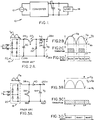
- a converter 10 is shown in Fig. 1 for converting voltage V S from an a.c. voltage source 12 to a voltage V D which is supplied to a load 14.
- the converter employs an energy storage capacitor 15 to make up the difference between the instantaneous energy flow between the load and the voltage source.
- the load may be a power supply, an electric motor, a resistance, etc.
- the voltage V D may be a d.c. voltage, or the input of an inverter (not shown) that supplies an a.c. voltage, for example, to an a.c. motor M.
- the conduction angle be 180 degrees (full conduction) and the current waveshapes within the circuit be the same as the input voltage waveshape. Thus, full conduction is prerequisite to a high power factor.
- converters of a basic design typically employ various types of diode bridge and SCR bridge circuits.
- One reason for this is because such circuits are inexpensive.
- these circuits draw power from the voltage input line to which the converter is connected for only a very short interval of each voltage cycle. The result is both a low power-factor and a high crest factor of input current; i.e., I peak /I rms .
- buck circuits 16 see Fig. 2a
- boost circuits 18 see Fig. 3a
- Each circuit has a full-wave rectifier section 20 at its interface with the input voltage source.
- an insulated gate bipolar transistor (IGBT) 22 has its drain-source circuit series connected between output 24a of the rectifier section and one terminal 26a of the converter output.
- IGBT insulated gate bipolar transistor
- other types of controlled power devices such as MOSFETs, bipolar devices, MCTs, etc., may be used in place of transistor 22.
- An inductor 28 is in-line connected between the transistor's source and the terminal.
- the other output 24b of the rectifier section is connected to the other output terminal 26b of the converter.
- a filter capacitor 30 is connected in parallel across outputs 24a, 24b, a diode 32 is connected in parallel between the source of transistor 22 and output 24b, and a storage capacitor 34 is connected in parallel across the output terminals.
- the converter output voltage V D is developed across capacitor 34.
- Output voltage V D is shown in Fig. 2b as a constant amplitude level d.c. voltage, while the rectified output voltage V R from section 20 is cyclical, having a peak amplitude level V P exceeding the constant amplitude level of output voltage V D .
- transistor 22 is in conduction only during that portion of each voltage cycle in which the amplitude of V R exceeds that of V D .
- the resultant period of conduction is only a fraction of each input voltage cycle.
- the conduction angle changes with the level of V D , rapidly decreasing as V D approaches the peak voltage V P .
- a "buck" type converter 16 cannot have a high power-factor (i.e., PF 0.9) unless V D is restricted to low values relative to V P .
- the drain-source circuit of an IGBT 36 is connected across the outputs 38a, 38b of rectifier section 20.
- a diode 40 is connected in series between output 38a and converter output terminal 42a, while output 38b is connected to output terminal 42b.
- An energy storage capacitor 44 is connected across the output terminals, and the converter output voltage V D is developed across this capacitor.
- the constant amplitude level of the converter output voltage exceeds the peak level V P of the rectifier section output throughout the voltage cycle. Consequently, transistor 36 is conducting for almost the entire cycle. While converter 18 produces a full conduction angle and thus a very high power-factor, the output voltage can no longer be controlled in the low voltage range relative to V P .
- V D needs to be so controlled in motor drive and power supply applications, an additional means of voltage reduction thus becomes necessary, adding to the cost and complexity of the converter. Also, this type of converter requires additional components to limit the output short-circuit current. In addition, there is an initial power surge into capacitor 44 whenever power is applied to the circuit. This surge is ultimately detrimental to the operating life of the converter.
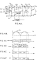
- Converter 50 is for use with, for example, appliance motor drives and power supplies to convert an a.c. input voltage V S to a d.c. output voltage V D .
- the converter has an input section 52 comprising a pair of terminals 54a, 54b which respectively connect to an a.c. voltage line.
- the a.c. voltage input to converter 50 is routed to a rectifier section 56.
- Respective inductors 58a, 58b are series connected in the lines from the input terminals to the rectifier section.
- the rectifier is a full-wave rectifier comprising diodes 60a-60d connected in the manner well-known in the art.
- the output of the rectifier section is a full-wave rectified sinusoidal voltage V R .
- Converter 50 next includes a first conversion means 62.
- This first conversion means 62 performs its voltage conversion during a portion of the input voltage cycle in which the input voltage level exceeds that of the output voltage level.
- means 62 includes a filter capacitor 64 connected in parallel with the output of rectifier section 56.
- An IGBT 65 transistor Q2 has its drain-source circuit connected in the high-voltage output path from the rectifier section. The gate of the transistor is connected to a control circuit 66 which will be described in more detail hereinafter.
- a diode 68 is connected in parallel between the source of transistor 65 and capacitor 64.
- the converter further includes a second conversion means 70.
- This second conversion means performs its voltage conversion during a portion of the input voltage cycle in which the output voltage level exceeds that of the input voltage level.
- Means 70 includes an inductor 72 connected between a node 74 (to which the source of transistor 65 and the anode of diode 68 are also attached) and a node 76.
- the drain of an IGBT 78 (transistor Q1) is also connected to node 76.
- a diode 80 is connected between node 76 and an output terminal 82a of the converter.
- the source of transistor 78 is connected both to the cathode of diode 68 as well as to the other converter output terminal 82b.
- the gate of transistor 78 is connected to control circuit 66.
- An energy storage output capacitor 84 is connected across the output terminals and the converter output voltage V D is developed across this capacitor.
- transistors 65 and 78 that besides being IGBTs, they can also be implemented using MOSFETs, MCTs, bipolar transistors, and other, similar types of semiconductor devices. Further, these devices can be used singly, or in serial and parallel combinations, all as is well-known in the art.
- Figs. 4b-4d it is a feature of converter 50 that for an output voltage V D as shown, the converter operates in a step-down or "buck" mode for that portion of the line cycle in which the input voltage is higher than the output voltage. For the portion of the cycle when the input voltage is lower than the output voltage the converter operates in the step-up or "boost” mode. This is done to realize a nearly full conduction angle for any level of output voltage in a range from zero to voltage levels higher than the peak of input voltage.
- converter 50 combines the most desirable features of both buck-type and boost-type converters without excessive stress on its power devices or an inversion of voltage polarity. It will be noted that while similar benefits might be obtainable, for example, by sequentially connecting a conventional boost and a conventional buck converter, such an arrangement would require intermediate energy storage capability in the form of an additional large capacitor. This would add to the overall cost of such a converter. The resulting sequential connection would, in effect, process the power twice resulting in greater losses in the system. These losses would not only reduce the overall efficiency of the power conversion, but decrease its cost-effectiveness because of a larger heat sink needed to dissipate the additional losses.
- control circuit 66 utilizes pulse-width modulation (PWM), which is well-known in the art, to control the instantaneous power conversion.
- PWM pulse-width modulation
- the control circuit further utilizes a steering circuit, which is unique to control circuit 66, to direct PWM signals to transistor 65 when the input voltage amplitude is greater than the output voltage amplitude, and to transistor 78 when the input voltage amplitude is less than the output voltage amplitude.
- the steering circuit insures that transistor 78 is switched OFF for the entire duration that transistor 65 pulse width modulates, and that transistor 65 is switched ON for the entire duration transistor 78 pulse width modulates.
- Figs. 4e and 4f illustrate the respective behaviors of transistors 78 (Q1) and 65 (Q2) when controlled by the steering circuit.
- Fig. 4d which illustrates the time sharing between operational modes
- the amount of time the converter is in one operational mode as compared to the other is not fixed; but rather, is time varying depending upon sensed changes between the characteristics of the actual converter output voltage and the preselected set of characteristics. Therefore, anything which may alter the voltage characteristics of the output voltage (a change in the load to which the voltage is applied, fluctuations in input line voltage characteristics, etc.), will immediately change the amount of time one converter section is performing the conversion, as compared to the other, all under the control of circuit 66.
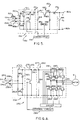
- the output votage V D of converter 50 is supplied to a voltage scaler 84, which could, for example, be a voltage divider network.
- the scaled output voltage V DS is applied to one input of a voltage amplifier 86 of the control circuit.
- a second input to the amplifier is a reference input V ref which is supplied by the system controller which can be, for example, a microprocessor 88.
- the microprocessor is programmed for the signal characteristics the converter output voltage should have based upon the characteristics of the input voltage waveform.
- Amplifier 86 compares the instantaneous output characteristics with those of its reference input, and provides as an output an error signal representing the differences between the two inputs.
- This error signal is supplied to one input of a multiplier 90.
- a current waveshape generator 92 has as its input the rectified input voltage waveform from rectifier section 56 of the converter. Alternatively, the input to the generator could also be supplied by other means.
- the waveform output of generator 92 is also provided as an input to multiplier 90.
- the multiplier combines the error signal output from voltage amplifier 86 with that of the waveform generator, amplifies (multiplies) the result, and supplies this resultant waveform to one input of a sensed current amplifier 94.
- Amplifier 94 has as a second input one output from a current scaling module 95 which is a scaled and filtered version of the input current waveform to the converter. The amplifier compares the two waveforms and produces an error signal representing the differences between the two inputs.
- An oscillator 96 is programmed to generate a waveform, for example, a sawtooth waveform Ws. It is common practice to operate the oscillator at a fixed, preselected frequency known as the PWM carrier frequency. This has the disadvantage of concentrating all the electro-magnetic interference (EMI) in a narrow frequency band. This, in turn, results in higher cost EMI filters. EMI noise can be more evenly spread throughout the frequency spectrum if the PWM carrier frequency is varied slowly in a continuous manner, for example, in accordance with the rectified output, resulting in a more economical realization of the EMI filter.
- One output from the oscillator is supplied as the non-inverting input of a comparator 98.
- the output from current amplifier 94 is supplied to the inverting input of the comparator.
- the output from comparator 98 is applied to one reset input of a latch 100.
- Oscillator 96 supplies its output to the set input S of the latch, in addition to supplying it to comparator 98.
- Latch 100 operates so there is a transition in its Q output from one logic state to another upon the occurrence of an element of waveform Ws at its set input S.
- the error signal from comparator 98 By applying the error signal from comparator 98 to a reset input R1 of the latch, the Q output of the latch is reset to its initial logic state. Because the error signal changes, its application to latch 100 effectively varies the duty cycle of the output signal from the latch, generating the basic pulse-width modulated signal used to control the power conversion process.
- a second comparator 102 has as one input the scaled, but instantaneous level of the input current to the converter, this input being supplied by the current module 95. Comparator 102 has as its other input a fixed value representing the maximum permissible peak value of the input current. The output of this comparator is applied to a second reset input R2 of latch 100 to reduce the duty cycle of the latch output if the peak input current exceeds the maximum permissible value and overrides the normal PWM signal to protect against excessive peak currents in the converter input circuit.
- An AND gate 104 has multiple inputs. One input is the inverted waveform output from oscillator 96. A second input is the variable duty cycle output of latch 100. These two inputs to the gate combine to produce a PWM output signal from the gate. A third input is from a comparator 106 having as one input a system shut-down signal. A fourth input is from a power supply monitor circuit 108 for the converter. This circuit includes comparators 110 and 112, and a voltage reference 114. The circuit determines if the power supply level for the converter circuitry is within specified operating limits. It will be understood that the inputs to gate 104 from comparator 106 and power supply monitor circuit 108 are used to override the otherwise normal operation of the control circuit.
- converter 50 uses its "buck" mode of operation. For this mode, transistor 78 is switched “off” by control circuit 66 and transistor 65 is supplied a pulse width modulated output from the control circuit. When the output voltage is above the rectified line voltage, the converter is in its "boost” mode and transistor 78 is supplied the pulse width modulated output signal. However, transistor 65, instead of being switched “off", is maintained in its conducting state.
- transistor 65 is series connected in one of the voltage lines and must be maintained in conduction when not pulse width modulated. Since the converter is working with high voltage levels, it is desirable to operate transistors 65 and 78 in such a way that the stresses incurred in switching are minimized. This promotes a higher degree of conversion efficiency and a longer operational life for the transistor.
- the time sharing strategy employed in control circuit 66 helps achieve this operational advantage.
- the pulse width modulated output from gate 104 is supplied to a steering circuit 116, and, more specifically, to a steering logic module 118.
- a comparator 120 has as one input the scaled and filtered output voltage from rectifier 56 of the converter, and as a second input the scaled output voltage from the converter. The comparator output is supplied as a second input to module 118.
- Module 118 comprises gating circuitry for steering the PWM output from gate 104.
- One output from module 118 is to a driver 122.
- the output of the driver is connected to the gate of transistor 78 and is used to switch the transistor "on" and "off”.
- a second output from the module is to a pulse generator 124.
- Generator 124 is responsive to the PWM input supplied to it to generate two signals for each pulse input.
- Generator 124 acts as a power conservator in that the pulses it generates are much shorter in duration than the width of an input pulse to the generator. Thus, the amount of energy contained in the outputs from generator 124 is much less than if the PWM input were supplied directly to transistor 65.
- the two pulses produced by generator 124 for each PWM input are provided to a level shifting circuit 126.
- transistor 65 requires a high voltage input.
- the circuitry employed within control circuit 66 operates at a low voltage level, approximately 5v d.c.
- Circuit 126 converts the low level input from generator 124 to the high level input required for operating transistor 65.
- the "on” and “off” outputs from circuit 126 are supplied to transistor 65 by a driver circuit 127 that operates at the same high voltage as the high line.
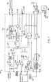
- an alternate embodiment of the converter of the present invention is indicated generally 150.
- the front end of this converter is similar to that of converter 50 in that it has an input section 152 and a full-wave rectifier section 156.
- the converter includes a first conversion means 170 which is a "boost"-type converter.
- This conversion means includes a transistor 178 whose drain-source circuit is connected across the output of rectifier section 156, the drain being connected to a node 176 at one side of the rectifier output.
- the gate of the transistor is connected to a control circuit 166 which functions in the same manner as the circuit 66 previously described.
- a diode 180 is connected between node 176 and a node 177.
- Converter 150 also includes a second conversion means 162 which is a "buck"-type converter.
- a filter capacitor 164 is connected between node 177 and the source of transistor 178.
- a transistor 165 has its drain-source circuit connected between node 177 and a node 179, this circuit being in-line with the high side of the voltage path through the converter.
- the gate of the transistor is connected to a driver circuit 185 which, in turn, is connnected to a control circuit 166.
- a diode 168 is connected in parallel between the source of transistor 165 and capacitor 164.
- An inductor 172 is series connected between node 179 and output terminal 182a of the converter; while, the cathode of diode 168 is also connected to output terminal 182b of the converter.
- An energy storage output capacitor 184 is connected across these output terminals and the converter output voltage V D is developed across this capacitor.
- converter 150 Operation of converter 150 is generally the same as that of converter 50, the major difference between the two embodiments being the reversal of the "buck" and “boost” converter sections.
- Converter 250 differs from the previously described embodiments in that the output from the converter is for use with a poly-phase a.c. load such as the three-phase motor M.
- the converter is similar to converter 150 with regard to its input section 252, rectifier section, and first converter section 270.
- converter 250 has a three-phase "buck" section 262.
- the section includes six transistors 265a-265f arranged in three pairs, one pair for each phase. Because the arrangement for the three phases is identical, only one is described. Thus, the drain of transistor 265a is connected to a node 281 on the high side voltage line of the converter.
- the source of its paired transistor 265b is connected to a node 283 on the low side voltage line.
- the source of transistor 265a is connected to a node 285 to which one input to motor M is connected.
- the drain of transistor 265b is also connected to this node.
- the gates of the transistors are connected to a driver circuit 227 and thus to a control circuit 266 which, again, functions in the manner described with respect to control circuit 66. Beside the pulse-width modulation control feature described with respect to circuit 66, control circuit 266 and converter section 262 act to convert the d.c. output voltage from the converter to provide an a.c. output to each motor phase.
- Fig. 6B discloses a converter 350 which is similar to the converter 250 of Fig. 6A, except for the front end portion of the converter. For this reason, only this portion of the converter is shown.
- the main feature of converter 350 is that it combines both the rectifier section and first conversion means, "boost section", of the converter into one section, thereby reducing the number of parts required for the converter.
- input section 352 is similar to that previously described, as is the second converter "buck" section 362.
- converter section 356 comprises a dual fast diode module 359 comprising diodes 360a, and 360c. Diodes packaged such as diodes 360a, 360c in a module 359 are currently, commercially available. The diodes comprise two legs of a full-wave rectifier as previously described.
- the other two legs of the rectifier include MOSFET transistors 378a, 378b. Respective diodes 360b, and 360d are connected across the drain-source paths of the two transistors to complete the other two legs of the rectifier.
- the gate of each transistor is connected to a control circuit 366, and operation of the transistors is as previously described with respect to transistor 78 to perform the "boost" conversion function of the converter.
- MOSFETs packaged with diodes such as 360b, and 360d are also currently, commercially available. Thus, the number of parts required to achieve both the rectification and "boost" functions of a converter 350 has been reduced to three.
- the output from section 356 is applied across a capacitor 364 within section 362.
- the pulse-width modulation and unique time sharing arrangement described has several advantages over an arrangement in which a conventional boost converter and a conventional buck converter are sequentially arranged. Since a combination of these conventional converter elements would require intermediate energy storage capability and dual processing of power, the converter of the present invention provides not only a lower cost system but also one which is more efficient.
Landscapes
- Engineering & Computer Science (AREA)
- Power Engineering (AREA)
- Rectifiers (AREA)
- Dc-Dc Converters (AREA)
- Control Of Motors That Do Not Use Commutators (AREA)
- Control Of Ac Motors In General (AREA)
Applications Claiming Priority (2)
| Application Number | Priority Date | Filing Date | Title |
|---|---|---|---|
| US07/670,031 US5235504A (en) | 1991-03-15 | 1991-03-15 | High power-factor converter for motor drives and power supplies |
| US670031 | 1991-03-15 |
Publications (2)
| Publication Number | Publication Date |
|---|---|
| EP0504094A2 true EP0504094A2 (de) | 1992-09-16 |
| EP0504094A3 EP0504094A3 (en) | 1992-11-25 |
Family
ID=24688697
Family Applications (1)
| Application Number | Title | Priority Date | Filing Date |
|---|---|---|---|
| EP19920630025 Withdrawn EP0504094A3 (en) | 1991-03-15 | 1992-03-05 | High power factor converter for motor drives and power supplies |
Country Status (5)
| Country | Link |
|---|---|
| US (1) | US5235504A (de) |
| EP (1) | EP0504094A3 (de) |
| JP (1) | JP3274169B2 (de) |
| KR (1) | KR100296200B1 (de) |
| CA (1) | CA2062698C (de) |
Cited By (21)
| Publication number | Priority date | Publication date | Assignee | Title |
|---|---|---|---|---|
| EP0585948A1 (de) * | 1992-09-04 | 1994-03-09 | Siemens Aktiengesellschaft | Schaltungsanordnung zur Umsetzung der Wechselspannung eines Versorgungsnetzes in eine Ausgleichsspannung mit einer im wesentlichen sinusförmigen, netzfrequenten Stromaufnahme |
| EP0580198A3 (en) * | 1992-07-03 | 1994-06-15 | Philips Electronics Nv | Power supply circuit with standby arrangement |
| FR2700081A1 (fr) * | 1992-12-30 | 1994-07-01 | Unite Hermetique Sa | Structure d'un convertisseur statique de fréquence. |
| CN1037307C (zh) * | 1992-07-03 | 1998-02-04 | 菲利浦电子有限公司 | 带备用设置的电源电路 |
| EP0779700A3 (de) * | 1995-12-11 | 1998-12-23 | Lockheed Martin Corporation | Gleichstromversorgung mit verbessertem Leistungsfaktor |
| EP0786857A4 (de) * | 1995-07-11 | 1999-12-29 | Meidensha Electric Mfg Co Ltd | Wandlerschaltkreis mit sinusförmiger stromaufnahme |
| WO2000007414A1 (en) * | 1998-07-29 | 2000-02-10 | Koninklijke Philips Electronics N.V. | Preconditioner |
| DE19854567A1 (de) * | 1998-11-26 | 2000-06-08 | Danfoss Compressors Gmbh | Verfahren zum Steuern einer Gleichrichterschaltung und Gleichrichterschaltung |
| US6528956B2 (en) | 2000-09-15 | 2003-03-04 | Lightech Electronics Industries Ltd. | Electronic ballast for high-intensity discharge lamps |
| WO2003041456A1 (en) * | 2001-11-05 | 2003-05-15 | Lightech Electronics Industries Ltd. | Electronic ballast for high-intensity discharge lamps |
| EP1087515A3 (de) * | 1999-09-22 | 2005-02-02 | Ford Motor Company | Motorregelkreis |
| EP1451921A4 (de) * | 2001-11-02 | 2006-01-11 | Aker Wade Power Technologies L | Schnelles ladegerät für batterien mit hoher kapazität |
| EP1858145A1 (de) * | 2006-05-15 | 2007-11-21 | Austriamicrosystems AG | Spannungsgenerator- Anordnung und Verfahren zur Spannungsumwandlung |
| US7301308B2 (en) | 2001-11-02 | 2007-11-27 | Aker Wade Power Technologies, Llc | Fast charger for high capacity batteries |
| WO2009000465A1 (de) * | 2007-06-22 | 2008-12-31 | Tridonicatco Gmbh & Co. Kg | Leistungsfaktor-korrekturschaltung für ein elektronisches vorschaltgerät für ein leuchtmittel |
| US7551462B2 (en) | 2005-02-08 | 2009-06-23 | Hitachi, Ltd. | Soft switching DC-DC converter including a buck converter and a boost converter sharing a common transformer |
| DE102008016472A1 (de) * | 2008-03-31 | 2009-10-01 | BSH Bosch und Siemens Hausgeräte GmbH | Schaltungsanordnung zum Betreiben einer elektrischen Maschine eines Hausgeräts und entsprechendes Verfahren |
| DE19861339B4 (de) * | 1998-11-02 | 2012-04-12 | Eppendorf Ag | Elektronische Handpipettiervorrichtung |
| FR2983365A1 (fr) * | 2011-11-25 | 2013-05-31 | Renault Sa | Systeme de transfert d'energie electrique |
| EP2642653A1 (de) * | 2012-03-20 | 2013-09-25 | C. & E. Fein GmbH | Treiberschaltung und Ansteuerverfahren |
| EP3026812A1 (de) | 2014-11-27 | 2016-06-01 | Carel Industries S.p.A. | Vorrichtung zum betreiben eines elektromotors und verfahren zum betreiben einer antriebsvorrichtung |
Families Citing this family (88)
| Publication number | Priority date | Publication date | Assignee | Title |
|---|---|---|---|---|
| US5402331A (en) * | 1992-02-25 | 1995-03-28 | Matsushita Electric Works | Power device |
| WO1993026078A1 (en) * | 1992-06-10 | 1993-12-23 | Digital Equipment Corporation | High power factor switched dc power supply |
| EP0881758B1 (de) * | 1994-04-08 | 2004-06-23 | Vlt Corporation | Leistungswandlung mit hohem Wirkungsgrad |
| US6768279B1 (en) | 1994-05-27 | 2004-07-27 | Emerson Electric Co. | Reprogrammable motor drive and control therefore |
| US5572417A (en) * | 1994-07-13 | 1996-11-05 | Vlt Corporation | AC to DC boost power converters |
| CA2151532C (en) * | 1994-07-25 | 1998-12-22 | Emerson Electric Co. | Auxiliary starting switched reluctance motor |
| US5606232A (en) * | 1994-11-22 | 1997-02-25 | Nidec Corporation | DC on line AC brushless motor |
| US5615101A (en) * | 1994-12-29 | 1997-03-25 | Lucent Technologies Inc. | Power converter with high power factor |
| US5747972A (en) * | 1995-01-11 | 1998-05-05 | Microplanet Ltd. | Method and apparatus for electronic power control |
| US7315151B2 (en) * | 1995-01-11 | 2008-01-01 | Microplanet Inc. | Method and apparatus for electronic power control |
| US5646513A (en) * | 1995-03-10 | 1997-07-08 | International Business Machines Corporation | Dynamic loop compensator for continuous mode power converters |
| US5703456A (en) * | 1995-05-26 | 1997-12-30 | Emerson Electric Co. | Power converter and control system for a motor using an inductive load and method of doing the same |
| US5608301A (en) * | 1995-06-28 | 1997-03-04 | Hitachi Koki Co., Ltd. | Motor control system for centrifugal machine |
| US5731681A (en) * | 1995-06-28 | 1998-03-24 | Hitachi Koki Co., Ltd. | Motor control system for centrifugal machine |
| US5636114A (en) * | 1995-11-30 | 1997-06-03 | Electronic Measurements, Inc. | Lossless snubber circuit for use in power converters |
| US5856919A (en) * | 1995-12-29 | 1999-01-05 | Lucent Technologies Inc. | Quasiresonant boost power converter with bidirectional inductor current |
| US5780949A (en) * | 1996-01-29 | 1998-07-14 | Emerson Electric Co. | Reluctance machine with auxiliary field excitations |
| US5866964A (en) * | 1996-01-29 | 1999-02-02 | Emerson Electric Company | Reluctance machine with auxiliary field excitations |
| US5923142A (en) * | 1996-01-29 | 1999-07-13 | Emerson Electric Co. | Low cost drive for switched reluctance motor with DC-assisted excitation |
| US5793626A (en) * | 1996-05-29 | 1998-08-11 | Lucent Technologies Inc. | High efficiency bimodal power converter and method of operation thereof |
| US5661645A (en) | 1996-06-27 | 1997-08-26 | Hochstein; Peter A. | Power supply for light emitting diode array |
| US5912812A (en) * | 1996-12-19 | 1999-06-15 | Lucent Technologies Inc. | Boost power converter for powering a load from an AC source |
| US6150771A (en) * | 1997-06-11 | 2000-11-21 | Precision Solar Controls Inc. | Circuit for interfacing between a conventional traffic signal conflict monitor and light emitting diodes replacing a conventional incandescent bulb in the signal |
| US5994869A (en) * | 1997-12-05 | 1999-11-30 | General Electric Company | Power conversion circuit for a motor |
| US5923143A (en) * | 1998-03-20 | 1999-07-13 | York International Corporation | Solid state motor starter with energy recovery |
| US6043999A (en) * | 1998-05-21 | 2000-03-28 | Inventio Ag | Apparatus and method for controlling an elevator power supply |
| US6023037A (en) | 1998-11-05 | 2000-02-08 | Lincoln Global, Inc. | Electric ARC welder and plasma cutter |
| US6275405B1 (en) * | 1998-12-11 | 2001-08-14 | General Electronics Applications, Inc. | Motor drive circuit |
| DE19909464C2 (de) * | 1999-03-04 | 2001-03-22 | Danfoss Compressors Gmbh | Verfahren zur Erzeugung einer geregelten Gleichspannung aus einer Wechselspannung und Stromversorgungseinrichtung zur Durchführung des Verfahrens |
| DE60040721D1 (de) * | 1999-08-03 | 2008-12-18 | Nxp Bv | Aufwärts/abwärtsgleichstromwandler |
| US6091612A (en) * | 1999-08-04 | 2000-07-18 | Lincoln Global, Inc. | Universal power supply for arc welder |
| US6404346B1 (en) * | 1999-08-13 | 2002-06-11 | York International Corporation | Method and apparatus for detecting a failed thyristor |
| US6094035A (en) * | 1999-08-20 | 2000-07-25 | Gain Technology Corporation | Amplifying power converter circuits |
| DE19946242A1 (de) * | 1999-09-27 | 2001-04-05 | Grundfos As | Frequenzumrichter für einen Elektromotor |
| US6204649B1 (en) * | 2000-03-16 | 2001-03-20 | Micrel Incorporated | PWM regulator with varying operating frequency for reduced EMI |
| US6487098B2 (en) | 2001-02-01 | 2002-11-26 | International Business Machines Corporation | Power factor correction (PFC) circuit that eliminates an inrush current limit circuit |
| US6567283B2 (en) * | 2001-03-30 | 2003-05-20 | Youtility Inc. | Enhanced conduction angle power factor correction topology |
| US6549438B2 (en) * | 2001-04-30 | 2003-04-15 | Precision Automation, Inc. | AC-to-DC converter circuit utilizing IGBT's for improved efficiency |
| US7130205B2 (en) * | 2002-06-12 | 2006-10-31 | Michigan State University | Impedance source power converter |
| US7061195B2 (en) * | 2002-07-25 | 2006-06-13 | International Rectifier Corporation | Global closed loop control system with dv/dt control and EMI/switching loss reduction |
| KR100720750B1 (ko) | 2002-07-25 | 2007-05-23 | 인터내쇼널 렉티파이어 코포레이션 | dv/dt제어와 EMI/스위칭 손실 감소를 구비한 광역폐루프 제어 시스템 |
| US6839253B2 (en) * | 2003-02-06 | 2005-01-04 | Zippy Technology Corp. | Multi-period cycle-alternative switching mode power supply control device |
| US7224592B2 (en) * | 2003-02-06 | 2007-05-29 | Zippy Technology Corp. | Multi-period cycle-alternative switching mode power supply control device and its control method |
| US7193826B2 (en) * | 2004-02-27 | 2007-03-20 | York International Corporation | Motor disconnect arrangement for a variable speed drive |
| US7231773B2 (en) * | 2004-04-12 | 2007-06-19 | York International Corporation | Startup control system and method for a multiple compressor chiller system |
| US7164242B2 (en) * | 2004-02-27 | 2007-01-16 | York International Corp. | Variable speed drive for multiple loads |
| US7207183B2 (en) * | 2004-04-12 | 2007-04-24 | York International Corp. | System and method for capacity control in a multiple compressor chiller system |
| US7793509B2 (en) | 2004-04-12 | 2010-09-14 | Johnson Controls Technology Company | System and method for capacity control in a multiple compressor chiller system |
| US8785816B2 (en) | 2004-07-13 | 2014-07-22 | Lincoln Global, Inc. | Three stage power source for electric arc welding |
| US9956639B2 (en) * | 2005-02-07 | 2018-05-01 | Lincoln Global, Inc | Modular power source for electric ARC welding and output chopper |
| US8269141B2 (en) | 2004-07-13 | 2012-09-18 | Lincoln Global, Inc. | Power source for electric arc welding |
| US8581147B2 (en) | 2005-03-24 | 2013-11-12 | Lincoln Global, Inc. | Three stage power source for electric ARC welding |
| US20070194721A1 (en) * | 2004-08-20 | 2007-08-23 | Vatche Vorperian | Electronic lighting ballast with multiple outputs to drive electric discharge lamps of different wattage |
| US9855620B2 (en) | 2005-02-07 | 2018-01-02 | Lincoln Global, Inc. | Welding system and method of welding |
| US9647555B2 (en) * | 2005-04-08 | 2017-05-09 | Lincoln Global, Inc. | Chopper output stage for arc welder power source |
| US8134329B2 (en) * | 2006-04-13 | 2012-03-13 | International Rectifier Corporation | Buck converter with improved filter design |
| US7777459B2 (en) * | 2006-12-30 | 2010-08-17 | Advanced Analogic Technologies, Inc. | High-efficiency DC/DC voltage converter including capacitive switching pre-converter and down inductive switching post-regulator |
| US7812579B2 (en) * | 2006-12-30 | 2010-10-12 | Advanced Analogic Technologies, Inc. | High-efficiency DC/DC voltage converter including capacitive switching pre-converter and up inductive switching post-regulator |
| US8217616B2 (en) * | 2007-11-02 | 2012-07-10 | HJamilton Sundstrand Corporation | Electric motor control with buck boost converter |
| US8264188B2 (en) * | 2008-07-31 | 2012-09-11 | Illinois Tool Works Inc. | Voltage regulated DC supply circuit for a wire feed drive system |
| CN101594053B (zh) * | 2009-03-27 | 2011-08-17 | 广州金升阳科技有限公司 | 一种宽范围电压输入的电源转换器 |
| EP2523338A4 (de) * | 2010-01-05 | 2015-08-05 | Hitachi Ltd | Wechselstrom-gleichstrom-wandler und verfahren zu dessen steuerung |
| US8415936B2 (en) * | 2010-07-19 | 2013-04-09 | Intersil Americas Inc. | Multiphase DC-DC converter using zero voltage switching |
| US8760071B2 (en) | 2010-10-29 | 2014-06-24 | Abl Ip Holding Llc | Drive circuit for light emitting diode array based on a buck-boost topology |
| US8742676B2 (en) | 2010-10-29 | 2014-06-03 | Abl Ip Holding Llc | Drive circuit for light emitting diode array based on sepic or cuk topology |
| US8901901B2 (en) * | 2011-02-10 | 2014-12-02 | Pai Capital Llc | Digital phase adjustment for multi-phase power converters |
| JP5525494B2 (ja) * | 2011-08-29 | 2014-06-18 | シャープ株式会社 | 力率改善回路 |
| US9293984B2 (en) * | 2011-08-29 | 2016-03-22 | Sharp Kabushiki Kaisha | Illumination apparatus and power supply circuit |
| JP2013048514A (ja) * | 2011-08-29 | 2013-03-07 | Sharp Corp | 力率改善回路 |
| US10333424B2 (en) * | 2012-02-01 | 2019-06-25 | Schneider Electric It Corporation | Offline power supply |
| JP5803945B2 (ja) * | 2012-05-10 | 2015-11-04 | 株式会社日本自動車部品総合研究所 | 電力変換装置 |
| US10384289B2 (en) | 2012-06-08 | 2019-08-20 | Illinois Tool Works Inc. | Welding wire feeder bus control system and method |
| US10105781B2 (en) | 2012-06-08 | 2018-10-23 | Illinois Tool Works Inc. | Welding system inrush current control system and method |
| US9878393B2 (en) | 2012-06-08 | 2018-01-30 | Illinois Tool Works Inc. | Welding wire feeder power control system and method |
| US9662735B2 (en) | 2012-06-08 | 2017-05-30 | Illinois Tool Works Inc. | Welding wire feeder power application system and method |
| US10406621B2 (en) | 2012-06-08 | 2019-09-10 | Illinois Tool Works Inc. | Polarity sensing welding wire feeder system and method |
| US9463523B2 (en) | 2012-06-08 | 2016-10-11 | Illinois Tool Works Inc. | Controlled waveform welding wire feeder system and method |
| SG10201704824RA (en) * | 2012-09-27 | 2017-07-28 | Daikin Ind Ltd | Direct ac power converter |
| JP6279423B2 (ja) * | 2014-07-29 | 2018-02-14 | 三菱電機株式会社 | 電力変換装置 |
| US9419551B2 (en) * | 2014-09-17 | 2016-08-16 | Arm Limited | Motor driver and a method of operating thereof |
| US11491573B2 (en) | 2015-08-17 | 2022-11-08 | Illinois Tool Works Inc. | Portable advanced process module |
| US11479139B2 (en) | 2015-09-11 | 2022-10-25 | Invertedpower Pty Ltd | Methods and systems for an integrated charging system for an electric vehicle |
| EP3347963A4 (de) | 2015-09-11 | 2019-01-16 | Invertedpower Pty Ltd | Steuergerät für eine induktive last mit einer oder mehreren induktiven wicklungen |
| WO2018204964A1 (en) | 2017-05-08 | 2018-11-15 | Invertedpowder Pty Ltd | A vehicle charging station |
| JP6409982B2 (ja) * | 2015-09-30 | 2018-10-24 | 富士電機株式会社 | 多相電力変換装置の制御回路 |
| US11018610B2 (en) | 2017-01-27 | 2021-05-25 | Franklin Electric Co., Inc. | Motor drive system and method |
| US10742467B1 (en) * | 2019-07-10 | 2020-08-11 | United States Of America As Represented By Secretary Of The Navy | Digital dynamic delay for analog power savings in multicarrier burst waveforms |
| CN119483274B (zh) * | 2025-01-16 | 2025-05-23 | 深圳市微源半导体股份有限公司 | 供电电路及电压变换器 |
Family Cites Families (14)
| Publication number | Priority date | Publication date | Assignee | Title |
|---|---|---|---|---|
| JPS602873B2 (ja) * | 1978-04-17 | 1985-01-24 | ソニー株式会社 | スイツチング安定化電源回路 |
| FR2497421A1 (fr) * | 1980-12-29 | 1982-07-02 | Thomson Csf | Circuit regulateur a decoupage non inverseur de tension |
| DE3104965A1 (de) * | 1981-02-12 | 1982-08-26 | Brown, Boveri & Cie Ag, 6800 Mannheim | Gleichstrompulswandler |
| US4412277A (en) * | 1982-09-03 | 1983-10-25 | Rockwell International Corporation | AC-DC Converter having an improved power factor |
| JPS60215222A (ja) * | 1984-04-11 | 1985-10-28 | Fuji Photo Film Co Ltd | 直流電源回路 |
| JPS6253178A (ja) * | 1985-08-30 | 1987-03-07 | Toshiba Corp | インバ−タ回路の電源装置 |
| DE3608082A1 (de) * | 1986-03-07 | 1987-09-10 | Licentia Gmbh | Schaltungsanordnung zur konstanthaltung der ausgangsgleichspannung bei wechselnder eingangsgleichspannung einer tiefsetz-hochsetzstellerkombination |
| US4729088A (en) * | 1987-05-11 | 1988-03-01 | Advance Transformer Company | Regulated high frequency power supply |
| US4964029A (en) * | 1988-05-18 | 1990-10-16 | Viteq Corporation | AC to DC power converter with input current waveform control for buck-boost regulation of output |
| JPH0252167A (ja) * | 1988-08-16 | 1990-02-21 | Showa Alum Corp | 金属材のろう付方法 |
| JPH0261059A (ja) * | 1988-08-24 | 1990-03-01 | Matsushita Electric Ind Co Ltd | 蒸着装置 |
| IT1225633B (it) * | 1988-11-30 | 1990-11-22 | Sgs Thomson Microelectronics | Protezione dai transitori di rete. |
| JPH037365A (ja) * | 1989-06-05 | 1991-01-14 | Nec Corp | 送り孔つき連続用紙用シリアルプリンタ |
| US5134355A (en) * | 1990-12-31 | 1992-07-28 | Texas Instruments Incorporated | Power factor correction control for switch-mode power converters |
-
1991
- 1991-03-15 US US07/670,031 patent/US5235504A/en not_active Expired - Fee Related
-
1992
- 1992-03-05 EP EP19920630025 patent/EP0504094A3/en not_active Withdrawn
- 1992-03-11 CA CA002062698A patent/CA2062698C/en not_active Expired - Fee Related
- 1992-03-13 JP JP08938492A patent/JP3274169B2/ja not_active Expired - Fee Related
- 1992-03-14 KR KR1019920004244A patent/KR100296200B1/ko not_active Expired - Fee Related
Cited By (33)
| Publication number | Priority date | Publication date | Assignee | Title |
|---|---|---|---|---|
| EP0580198A3 (en) * | 1992-07-03 | 1994-06-15 | Philips Electronics Nv | Power supply circuit with standby arrangement |
| CN1037307C (zh) * | 1992-07-03 | 1998-02-04 | 菲利浦电子有限公司 | 带备用设置的电源电路 |
| EP0585948A1 (de) * | 1992-09-04 | 1994-03-09 | Siemens Aktiengesellschaft | Schaltungsanordnung zur Umsetzung der Wechselspannung eines Versorgungsnetzes in eine Ausgleichsspannung mit einer im wesentlichen sinusförmigen, netzfrequenten Stromaufnahme |
| FR2700081A1 (fr) * | 1992-12-30 | 1994-07-01 | Unite Hermetique Sa | Structure d'un convertisseur statique de fréquence. |
| EP0605330A3 (de) * | 1992-12-30 | 1994-11-23 | Unite Hermetique | Struktur eines statischen Frequenzumwandlers. |
| US5592368A (en) * | 1992-12-30 | 1997-01-07 | L'unite Hermetique | Static frequency converter which compensates for fluctuations in a voltage source while controlling the waveform applied to a charge while controlling the waveform applied to a charge |
| EP0786857A4 (de) * | 1995-07-11 | 1999-12-29 | Meidensha Electric Mfg Co Ltd | Wandlerschaltkreis mit sinusförmiger stromaufnahme |
| EP0779700A3 (de) * | 1995-12-11 | 1998-12-23 | Lockheed Martin Corporation | Gleichstromversorgung mit verbessertem Leistungsfaktor |
| WO2000007414A1 (en) * | 1998-07-29 | 2000-02-10 | Koninklijke Philips Electronics N.V. | Preconditioner |
| DE19861339B4 (de) * | 1998-11-02 | 2012-04-12 | Eppendorf Ag | Elektronische Handpipettiervorrichtung |
| DE19854567A1 (de) * | 1998-11-26 | 2000-06-08 | Danfoss Compressors Gmbh | Verfahren zum Steuern einer Gleichrichterschaltung und Gleichrichterschaltung |
| EP1087515A3 (de) * | 1999-09-22 | 2005-02-02 | Ford Motor Company | Motorregelkreis |
| US6528956B2 (en) | 2000-09-15 | 2003-03-04 | Lightech Electronics Industries Ltd. | Electronic ballast for high-intensity discharge lamps |
| US7301308B2 (en) | 2001-11-02 | 2007-11-27 | Aker Wade Power Technologies, Llc | Fast charger for high capacity batteries |
| EP1451921A4 (de) * | 2001-11-02 | 2006-01-11 | Aker Wade Power Technologies L | Schnelles ladegerät für batterien mit hoher kapazität |
| WO2003041456A1 (en) * | 2001-11-05 | 2003-05-15 | Lightech Electronics Industries Ltd. | Electronic ballast for high-intensity discharge lamps |
| US7551462B2 (en) | 2005-02-08 | 2009-06-23 | Hitachi, Ltd. | Soft switching DC-DC converter including a buck converter and a boost converter sharing a common transformer |
| US7952332B2 (en) | 2006-05-15 | 2011-05-31 | Austriamicrosystems Ag | Voltage generator arrangement and method for voltage conversion |
| EP1858145A1 (de) * | 2006-05-15 | 2007-11-21 | Austriamicrosystems AG | Spannungsgenerator- Anordnung und Verfahren zur Spannungsumwandlung |
| WO2007131779A1 (en) * | 2006-05-15 | 2007-11-22 | Austriamicrosystems Ag | Voltage generator arrangement and method for voltage conversion |
| AT516394A5 (de) * | 2007-06-22 | 2016-05-15 | Tridonic Gmbh & Co Kg | Elektronisches vorschaltgerät mit pfc |
| CN102318173A (zh) * | 2007-06-22 | 2012-01-11 | 三多尼克爱特克两合股份有限公司 | 用于发光装置的电子镇流器的功率因数校正电路 |
| CN102318173B (zh) * | 2007-06-22 | 2015-01-14 | 三多尼克爱特克两合股份有限公司 | 具有功率因数校正电路的电子镇流器 |
| AT516394B1 (de) * | 2007-06-22 | 2016-05-15 | Tridonic Gmbh & Co Kg | Elektronisches vorschaltgerät mit pfc |
| WO2009000465A1 (de) * | 2007-06-22 | 2008-12-31 | Tridonicatco Gmbh & Co. Kg | Leistungsfaktor-korrekturschaltung für ein elektronisches vorschaltgerät für ein leuchtmittel |
| DE102008016472A1 (de) * | 2008-03-31 | 2009-10-01 | BSH Bosch und Siemens Hausgeräte GmbH | Schaltungsanordnung zum Betreiben einer elektrischen Maschine eines Hausgeräts und entsprechendes Verfahren |
| FR2983365A1 (fr) * | 2011-11-25 | 2013-05-31 | Renault Sa | Systeme de transfert d'energie electrique |
| EP2642653A1 (de) * | 2012-03-20 | 2013-09-25 | C. & E. Fein GmbH | Treiberschaltung und Ansteuerverfahren |
| CN103326572A (zh) * | 2012-03-20 | 2013-09-25 | C.&E.泛音有限公司 | 驱动器电路和驱动方法 |
| US9041335B2 (en) | 2012-03-20 | 2015-05-26 | C. & E. Fein Gmbh | Driver circuit and driving method |
| EP3026812A1 (de) | 2014-11-27 | 2016-06-01 | Carel Industries S.p.A. | Vorrichtung zum betreiben eines elektromotors und verfahren zum betreiben einer antriebsvorrichtung |
| CN105656391A (zh) * | 2014-11-27 | 2016-06-08 | 卡乐工业股份公司 | 电动机驱动装置、其启动方法和包括驱动装置的电机单元 |
| CN105656391B (zh) * | 2014-11-27 | 2018-07-03 | 卡乐工业股份公司 | 电动机驱动装置、其启动方法和包括驱动装置的电机单元 |
Also Published As
| Publication number | Publication date |
|---|---|
| JP3274169B2 (ja) | 2002-04-15 |
| KR920019100A (ko) | 1992-10-22 |
| US5235504A (en) | 1993-08-10 |
| CA2062698A1 (en) | 1992-09-16 |
| CA2062698C (en) | 1995-09-05 |
| JPH05176544A (ja) | 1993-07-13 |
| KR100296200B1 (ko) | 2001-10-24 |
| EP0504094A3 (en) | 1992-11-25 |
Similar Documents
| Publication | Publication Date | Title |
|---|---|---|
| US5235504A (en) | High power-factor converter for motor drives and power supplies | |
| Ahmed et al. | A new configuration of single-phase symmetrical PWM AC chopper voltage controller | |
| Bode et al. | Implementation of three level hysteresis current control for a single phase voltage source inverter | |
| Kim et al. | A PWM buck-boost AC chopper solving the commutation problem | |
| Kim et al. | New modulated carrier controlled PFC boost converter | |
| US6487098B2 (en) | Power factor correction (PFC) circuit that eliminates an inrush current limit circuit | |
| US6137700A (en) | Converter with a high power factor using a DC center point voltage | |
| US20010026460A1 (en) | Multiway power converter | |
| EP2985897B1 (de) | Stromwandler | |
| JPH0851790A (ja) | 誘導性負荷用制御回路 | |
| JP2004056997A (ja) | 高力率変換器システム及び方法 | |
| Ahmed | Modeling and simulation of ac–dc buck-boost converter fed dc motor with uniform PWM technique | |
| CA2207449A1 (en) | Mains rectifier circuit | |
| JP2000188867A (ja) | コンバータ回路および直流電圧制御用装置 | |
| Tu et al. | A new space-vector-modulated control for a unidirectional three-phase switch-mode rectifier | |
| JP2521345B2 (ja) | 定電圧・定周波数電源装置 | |
| US5991183A (en) | Polyphase voltage converter | |
| Consoli et al. | Unipolar converter for switched reluctance motor drives with power factor improvement | |
| JP3214687B2 (ja) | 降圧形高力率コンバータ | |
| KR20060023221A (ko) | 브릿지리스 역률개선회로 | |
| JPH1198847A (ja) | 整流回路 | |
| JP3690558B2 (ja) | 多相電圧形コンバータ | |
| Deshmukh et al. | Unity Power Factor Three Phase Induction Motor Drive Using Combined Extinction Angle and PWM Controlled Technique | |
| Oruganti et al. | Extension of inductor voltage control to three-phase buck-type ac-dc converter | |
| Ashraf et al. | An efficient single-phase ac-to-ac buck and boost matrix converter |
Legal Events
| Date | Code | Title | Description |
|---|---|---|---|
| PUAI | Public reference made under article 153(3) epc to a published international application that has entered the european phase |
Free format text: ORIGINAL CODE: 0009012 |
|
| AK | Designated contracting states |
Kind code of ref document: A2 Designated state(s): DE DK ES FR GB IT NL |
|
| PUAL | Search report despatched |
Free format text: ORIGINAL CODE: 0009013 |
|
| AK | Designated contracting states |
Kind code of ref document: A3 Designated state(s): DE DK ES FR GB IT NL |
|
| 18D | Application deemed to be withdrawn |
Effective date: 19930526 |