EP0505306A2 - Steuerungsschaltung für Halbduplex-Simplexschittstelle in einem Übertragungssystem - Google Patents
Steuerungsschaltung für Halbduplex-Simplexschittstelle in einem Übertragungssystem Download PDFInfo
- Publication number
- EP0505306A2 EP0505306A2 EP92480035A EP92480035A EP0505306A2 EP 0505306 A2 EP0505306 A2 EP 0505306A2 EP 92480035 A EP92480035 A EP 92480035A EP 92480035 A EP92480035 A EP 92480035A EP 0505306 A2 EP0505306 A2 EP 0505306A2
- Authority
- EP
- European Patent Office
- Prior art keywords
- simplex
- duplex
- data
- line
- control circuit
- Prior art date
- Legal status (The legal status is an assumption and is not a legal conclusion. Google has not performed a legal analysis and makes no representation as to the accuracy of the status listed.)
- Granted
Links
Images

Classifications
-
- H—ELECTRICITY
- H04—ELECTRIC COMMUNICATION TECHNIQUE
- H04L—TRANSMISSION OF DIGITAL INFORMATION, e.g. TELEGRAPHIC COMMUNICATION
- H04L5/00—Arrangements affording multiple use of the transmission path
- H04L5/14—Two-way operation using the same type of signal, i.e. duplex
- H04L5/16—Half-duplex systems; Simplex/duplex switching; Transmission of break signals non-automatically inverting the direction of transmission
Definitions
- This invention relates to data communications and more particularly to a circuit for controlling the interface between a half-duplex system using an electrical conductor and a simplex system using optical fibers.
- a well known type of data communication system uses a single electrical conductor, usually a coaxial cable, to connect a data terminal to a controller capable of supporting many terminals.
- the most common form of this system is a half-duplex system.
- a half-duplex system is one in which data can be transmitted only in one direction on the cable at any given time; that is, data cannot be transmitted in opposite directions on the cable at the same time.
- a controller transmits data to a terminal and waits for a response, indicating the terminal has received the data. If no response is received within a certain period of time, the controller assumes the data was not received and takes an appropriate action.
- the controller may, for example, re-transmit the data or may send an error message to a system operator.
- controller-transmitted data Since the controller initiates all communications with the terminal, only the controller or the terminal should transmit at any given time. There should be no collision on the cable between controller-transmitted data and terminal-transmitted data.
- a preamble (a series of signals which precede actual data) is conventionally employed.
- the preamble resets a receive clock and delineates the beginning of the data itself.
- a postamble a second series of signals which follow the actual data, is used to delineate the end of the message.
- a simplex system is one that uses separate conductors to carry transmitted and received data. Usually, data can be transmitted and received simultaneously over the separate conductors.
- half-duplex and simplex systems use the same media, there are components which can be used to prevent such echoing from occurring.
- devices known as hybrid transformers permit received simplex data to be applied to the half-duplex cable but not the local simplex transmitter.
- beam splitters can be used to transmit data to the half-duplex fiber but not to the local simplex optical transmitter.
- Neither of these solutions can be used in a hybrid system; that is, an electrical half-duplex system interfaced to an optical simplex system.
- a hybrid environment may exist where a terminal controller designed for electrical half-duplex operation is attached to a high-speed optical bus having dual transmit and receive optical fibers.
- the optical bus may be used either as a serial channel to a remote host processor or as a secure, high speed link to a supported terminal.
- United States Patent 4,288,869 assigned to the assignee of the present invention, addresses the problem of echoing in an electrical half-duplex/optical simplex interface.
- received simplex signals are applied to three parallel paths, each of which delays the signals by a different amount.
- the half-duplex system is connected to the path which introduces the intermediate amount of delay.
- the three paths provide inputs to a single NAND gate, the output of which is applied to a driver for the simplex transmitting fiber.
- the introduction of different amounts of delay into the received simplex signal prevents that signal from being passed through to the simplex transmitter.
- a sensitive optical receiver will emit noise signals when a nominally constant optical signal is received for a lengthy period of time.
- the noise may interfere with the proper functioning of the circuit shown in the referenced patent.
- the internal sampling levels in a sensitive receiver may be so disturbed that subsequent optical bits are not correctly translated to electrical bits.
- a continuous idle signal can cause problems since idle signals flowing in one direction would be collide with data flowing in the other direction.
- the present invention relates a control circuit for permitting keep-alive signals generated by a keep-alive source to be used at the interface between a half-duplex line and simplex lines.
- the control circuit includes a receive control logic circuit connected in parallel with the receiving simplex line and the half-duplex line.
- the circuit generates one of two control signals upon detection of predetermined bit patterns in the received signals.
- a gating means responds to the first control signal to set up a first connection between the receiving simplex line and the half-duplex line while blocking a second connection between the half-duplex line and the transmitting simplex line.
- the gating means responds to the second control signal to take down the first connection while partially setting up the second.
- the control circuit further includes a transmit control logic circuit connected in parallel with the half-duplex line and the transmitting simplex line.
- the transmit control circuit responds to predetermined bit patterns in received half-duplex data by generating either a third or a fourth control signal.
- a different gating means responds to the third control signal to complete the connection between the half-duplex line and the transmitting simplex line.
- This gating means responds to the fourth control signal to open the connection from the half-duplex line while gating the output of the keep-alive signal source onto the transmitting simplex line.
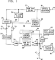
- FIG. 1 is a block diagram of a control circuit 10 which provides an interface between a half-duplex system, represented by a half-duplex electrical line 12, and a simplex optical system, represented by a receiving optical fiber 14 and a transmitting optical fiber 16.
- the half-duplex line 12 takes the form of an coaxial cable.
- the control circuit 10 performs the general function of controlling data received either from the half-duplex line 12 or the receiving simplex fiber 14 to permit the data to be routed through the interface without collisions or echoing.
- Data received on the simplex fiber 14 is applied to an optical receiver 18, which converts the optical signal to its electrical analog.
- the output of the optical receiver 18 is applied both to a receive control circuit 20, which will be described in detail later, and to a delay circuit 22.
- Delay circuit 22 which is preferably conventional, delays the received signal by a predetermined amount. For Manchester-encoded signals, a term which is explained below, the amount of the delay is one bit time or one-half of a two-bit cell.
- the output of delay circuit 22 is applied to a conventional clock circuit 24, which provides a clock signal having a bit rate frequency; that is twice the cell rate.
- the generated clock signal and the output of the delay circuit 22 are both applied to an electrical driver circuit 26, the output of which is connected to the half-duplex line 12 at a common connection point 28.
- the receive control circuit 20 provides an additional input to the driver circuit 26 and to an inverter 30.
- the general function of the receive control circuit 20 is to enable either the driver circuit 26 or an AND gate 32. If the signal level at the output of circuit 20 is such that driver circuit 26 is enabled, the inverted signal appearing at the output of inverter 30 will cause AND gate 32 to be disabled. Conversely, if the output of circuit 20 disables the driver circuit 26, the inverted signal produced by inverter 30 will cause AND gate 32 to be at least partially enabled.
- the interface circuit When data is being received on simplex fiber 14, the interface circuit, as described above, prevents that data from echoing to the transmitting simplex fiber 16 through a data path, including driver circuit 26, common connection 28, and an electrical receiver circuit 34.
- Data received from the half-duplex line 12 is always applied to the AND gate 32 through the electrical receiver circuit 34. If the AND gate 32 is already partially enabled by the output of inverter 30, the received half-duplex data is forwarded to a transmit control circuit 36 and to a one-bit delay circuit 38. Transmit control circuit 36 is connected to AND gates 40 and 44. Opposite logic-level signals are applied to these AND gates by the transmit control circuit 36. That is, if a high or enabling signal is applied to AND gate 40, a low or disabling signal is concurrently applied to AND gate 44. Conversely, if AND gate 44 receives an enabling signal from transmit control circuit 36, then AND gate 40 concurrently receives a disabling signal.
- a keep-alive oscillator 46 continuously generates a keep-alive signal, preferably a series of Manchester-encoded "1" signals which occur at the normal cell rate.
- the output of keep-alive oscillator 46 is either blocked or passed by AND gate 44, depending entirely on the state of the signal applied by transmit control circuit 36.
- AND gates 40 and 44 have a common connection 42 at the input to an driver circuit 48 for the transmitting simplex fiber 16.
- a "feedback" loop 94 connects point 42 to an input to the transmit control circuit 36 for reasons which are explained later.
- the basic function of the transmit control circuit 36 is to allow either keep-alive signals (from oscillator 46) to be gated to driver circuit 48 while blocking any signals occurring at the output of delay circuit 38 or, conversely, to block the keep-alive signal while forwarding data signals from the half-duplex line 12.
- Manchester codes are explained with reference to Figure 2.
- a conventional Manchester code requires that each binary signal (binary 1 or binary 0) be encoded in a two-bit cell having two signal level with a transition at the center of the cell. Transitions may or may not occur at the boundaries of the cell.
- a binary 1 may be represented by a cell having a falling center transition.
- Cells 50, 52, 54 and 56 are examples of valid binary 1 signals.
- a binary 0 may be represented by a cell having a rising center transition.
- Cells 58 and 60 are examples of valid binary 0 signals.
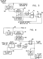
- Figure 3 is a schematic diagram of the receive control logic circuit 20. Output signals from the optical receiver 18 (shown in Figure 1) are applied both to a four stage shift register 66 and to a bit rate clock circuit 68. The clock circuit causes each bit in a received cell to be clocked into the shift register 66.
- Shift register 66 has four outputs, one from each of its four stages. The four outputs are connected in parallel to an exclusive OR circuit 70, the output of which is connected to the Reset input of a bistable latch 76. Outputs from the first and second stages are connected directly to an AND gate 74 while an output from stage 3 is connected to the same AND gate through an inverter 72.
- Figure 5 illustrates a bit stream that could be expected to occur at the output of optical receiver 18 during receipt of a unit of data.
- optical receiver will initially receive a string of binary 1 signals generated by a keep alive oscillator at circuitry at the opposite end of the optical fiber leading to optical receiver 18.
- the string represented by segment 110 of the bit stream, will be of indefinite length.
- exclusive OR circuit 70 Since different stages in the shift register will be storing different logic level signals during receipt of the idle signal, exclusive OR circuit 70 will not change states. Also, because the first and third stages of the shift register will be at the same level when an idle signal is being clocked through the register, the output of AND gate 74 remains low whenever an idle signal is being received.
- the latch 76 Since neither the AND gate 74 nor the exclusive OR circuit 70 can be driven high by the normal idle signal, the latch 76 remains unaffected in the presence of the idle signal. Latch 76, for reasons explained below, will be in its reset state as the idle signal is received and will produce a low level signal on its output line 78.
- the transmitter at the opposite end of the optical fiber inserts an intentional three bit Manchester code violation into the bit stream.
- the inserted code violation represented by segment 112, is an 011 bit pattern.
- the high level signal on line 78 closes the connection between half-duplex line 12 and receiving simplex fiber 14 by enabling electrical driver circuit 26.
- the high level signal simultaneously isolates the transmitting simplex fiber 16 from the half-duplex line 12 since inverter 30 drives the high level output to a low level or disabling input to AND gate 32.
- inverter 30 drives the high level output to a low level or disabling input to AND gate 32.
- Data received in a segment 114 is forwarded to the half-duplex line 12 through the driver 26 after a one bit delay in delay circuit 22.
- Data received in segment 114 may validly include the same 011 bit pattern which initially causes the latch 76 to become set. That does not pause a problem, however, since each occurrence of the 011 bit pattern will only attempt to drive the latch 76 to the same SET state it is already in.
- the data is followed by a postamble 116 consisting of four successive bits of the same level; i.e., either a 0000 or a 1111 bit pattern depending on whether the last data bit ended at a high or a low level.
- exclusive OR circuit 70 When four successive bits of the same level are clocked into register 66, exclusive OR circuit 70 generates a high level output. The high level output from OR circuit 70 resets latch 76 to provide a low level signal on line 78.
- the low level signal on line 78 disables driver circuit 26 and partially enables AND gate 32, which sets a partial connection between half-duplex data line 12 and simplex fiber 16.
- an edge detector is formed by a two stage shift register 80 (see figure 4), a high speed clock 82, an inverter 84 and an AND gate 86.
- Signal levels on half-duplex line 12 are forwarded through AND gate 32 to the data input of the shift register 80.
- High speed clock 82 frequently samples the signal level. When a rising transition occurs, a 0 level signal will be loaded into the second stage of the shift register 80 at the same time a 1 level signal is loaded into the first stage.
- AND gate 86 is driven by an inverted second stage output and a direct first stage output from register 80 and thus produces a high level output signal when a rising transition occurs in the signal received from the half-duplex line 12.
- the high level output signal from AND gate 86 sets a latch 88, to drive a Q output of the latch to a high level.
- the output of the latch 88 is applied directly to one input of an AND gate 90 and indirectly to the second input of the same AND gate through a one bit delay circuit 92.
- the one bit delay circuit 92 prevents the output of AND gate 90 from going high for a one bit period after latch 86 is set. Referring momentarily to Figure 1, it will be noted that data traveling between the half-duplex line 12 and the transmitting simplex fiber 16 is also delayed for a one bit period by a delay circuit 38.
- the one bit delay in triggering of AND gate 90 causes a corresponding delay in the partial enabling of AND gate 40; AND gate 40 is thus partially enabled by AND gate 90 coincident with the first arrival of data on the main data path.
- AND gate 40 will remain enabled while data is being provided by the half-duplex line 12. When the data ends, the line 12 will go to a nominally constant state and will cause what appears to be a string of half-bit 1's or half-bit 0's at the output of AND gate 40.
- a "pull-up" circuit consisting of a voltage source 41 and a resistor 43 will bias the point 42 at a high logic level in the absence of data.
Landscapes
- Engineering & Computer Science (AREA)
- Signal Processing (AREA)
- Computer Networks & Wireless Communication (AREA)
- Bidirectional Digital Transmission (AREA)
Applications Claiming Priority (2)
| Application Number | Priority Date | Filing Date | Title |
|---|---|---|---|
| US07/672,811 US5212685A (en) | 1991-03-21 | 1991-03-21 | Control circuit for half-duplex/simplex interface in communication system |
| US672811 | 1991-03-21 |
Publications (3)
| Publication Number | Publication Date |
|---|---|
| EP0505306A2 true EP0505306A2 (de) | 1992-09-23 |
| EP0505306A3 EP0505306A3 (en) | 1993-06-09 |
| EP0505306B1 EP0505306B1 (de) | 1997-09-24 |
Family
ID=24700100
Family Applications (1)
| Application Number | Title | Priority Date | Filing Date |
|---|---|---|---|
| EP92480035A Expired - Lifetime EP0505306B1 (de) | 1991-03-21 | 1992-02-26 | Steuerungsschaltung für Halbduplex-Simplexschnittstelle in einem Übertragungssystem |
Country Status (4)
| Country | Link |
|---|---|
| US (1) | US5212685A (de) |
| EP (1) | EP0505306B1 (de) |
| JP (1) | JPH0724400B2 (de) |
| DE (1) | DE69222336T2 (de) |
Families Citing this family (8)
| Publication number | Priority date | Publication date | Assignee | Title |
|---|---|---|---|---|
| JP3436631B2 (ja) * | 1996-02-22 | 2003-08-11 | 富士通株式会社 | 光送受信回路 |
| US6049548A (en) * | 1996-11-22 | 2000-04-11 | Stanford Telecommunications, Inc. | Multi-access CS-P/CD-E system and protocols on satellite channels applicable to a group of mobile users in close proximity |
| USD396044S (en) | 1997-03-04 | 1998-07-14 | Northrop Grumman Corporation | Modem |
| US5982755A (en) * | 1997-03-06 | 1999-11-09 | Nortel Networks Corporation | System and method for providing high terminal coupling loss in a handsfree terminal |
| US5959979A (en) * | 1997-05-05 | 1999-09-28 | Northrop Grumman Corporation | Half-duplex communication system for telemetry modems |
| EP1169800A4 (de) * | 1999-04-12 | 2002-10-23 | Samsung Electronics Co Ltd | Verfahren und vorrichtung zur getorten übertragung in einem cdma nachrichtenübertragungssystem |
| US6649898B1 (en) * | 2000-06-30 | 2003-11-18 | Intel Corporation | Method and apparatus for optically enabling a circuit component in a large scale integrated circuit |
| DE102014219512A1 (de) * | 2014-09-26 | 2016-03-31 | Dr. Johannes Heidenhain Gmbh | Verfahren und Vorrichtung zur seriellen Datenübertragung über einen bidirektionalen Datenübertragungskanal |
Family Cites Families (6)
| Publication number | Priority date | Publication date | Assignee | Title |
|---|---|---|---|---|
| US3979723A (en) * | 1975-10-29 | 1976-09-07 | International Business Machines Corporation | Digital data communication network and control system therefor |
| US4288869A (en) * | 1980-01-23 | 1981-09-08 | International Business Machines Corp. | Half-duplex/simplex digital signal converter |
| US4599719A (en) * | 1984-06-18 | 1986-07-08 | At&T Information Systems Inc. | Full duplex data set with half-duplex emulation |
| US4680750A (en) * | 1984-10-01 | 1987-07-14 | Lynch Communication Systems, Inc. | Universal high-speed span line switch |
| US4672601A (en) * | 1984-12-06 | 1987-06-09 | Motorola, Inc. | Duplex interconnect/dispatch trunked radio system |
| US4996683A (en) * | 1988-10-13 | 1991-02-26 | Toyoda Koki Kabushiki Kaisha | Optical transmission device |
-
1991
- 1991-03-21 US US07/672,811 patent/US5212685A/en not_active Expired - Fee Related
- 1991-12-02 JP JP3317922A patent/JPH0724400B2/ja not_active Expired - Lifetime
-
1992
- 1992-02-26 EP EP92480035A patent/EP0505306B1/de not_active Expired - Lifetime
- 1992-02-26 DE DE69222336T patent/DE69222336T2/de not_active Expired - Fee Related
Also Published As
| Publication number | Publication date |
|---|---|
| US5212685A (en) | 1993-05-18 |
| JPH04326828A (ja) | 1992-11-16 |
| DE69222336T2 (de) | 1998-03-26 |
| EP0505306A3 (en) | 1993-06-09 |
| JPH0724400B2 (ja) | 1995-03-15 |
| DE69222336D1 (de) | 1997-10-30 |
| EP0505306B1 (de) | 1997-09-24 |
Similar Documents
| Publication | Publication Date | Title |
|---|---|---|
| US4903016A (en) | Communication control unit | |
| US6363085B1 (en) | Universal serial bus repeater | |
| US4337465A (en) | Line driver circuit for a local area contention network | |
| US4345250A (en) | Information communication system with collision avoidance | |
| EP0476444B1 (de) | Optischer Sender/Empfänger | |
| JPS59500159A (ja) | 衝突検出を行う多点デ−タ通信システム | |
| US4380761A (en) | Digital phase decoder with collision detection | |
| CN110113070B (zh) | 一种适用于usb的信号发送及接收方法 | |
| EP0505306B1 (de) | Steuerungsschaltung für Halbduplex-Simplexschnittstelle in einem Übertragungssystem | |
| EP0172236B1 (de) | Verfahren und vorrichtung zum nachweis des zusammensturzes von datenpaketen | |
| JPH0228939B2 (de) | ||
| CA1324690C (en) | Optical fiber bus controller | |
| US20020118412A1 (en) | Network device including detection of link status employing auto-negotiation | |
| US5068820A (en) | Data transfer system having transfer discrimination circuit | |
| US5729547A (en) | Automatic driver/receiver control for half-duplex serial networks | |
| US7046722B2 (en) | Transceiver with means for error management | |
| US4835776A (en) | Communication filter | |
| US6993082B2 (en) | Station and method for operating a CAN communication line | |
| KR920000388B1 (ko) | 송·수신 데이타 충돌 감지회로 | |
| KR100256674B1 (ko) | 이더넷 근거리 통신망 구현을 위한 매칭 어뎁터 | |
| JP3252556B2 (ja) | 通信装置 | |
| JPH0637769A (ja) | マルチプルアクセスの通信システム | |
| JP3208930B2 (ja) | インテリジェントモデム | |
| KR100290677B1 (ko) | 피포디바이스의자동리스타트장치 | |
| KR100207482B1 (ko) | 스마트카드의 패리티검출장치 |
Legal Events
| Date | Code | Title | Description |
|---|---|---|---|
| PUAI | Public reference made under article 153(3) epc to a published international application that has entered the european phase |
Free format text: ORIGINAL CODE: 0009012 |
|
| AK | Designated contracting states |
Kind code of ref document: A2 Designated state(s): DE FR GB |
|
| 17P | Request for examination filed |
Effective date: 19930120 |
|
| PUAL | Search report despatched |
Free format text: ORIGINAL CODE: 0009013 |
|
| AK | Designated contracting states |
Kind code of ref document: A3 Designated state(s): DE FR GB |
|
| 17Q | First examination report despatched |
Effective date: 19960319 |
|
| GRAG | Despatch of communication of intention to grant |
Free format text: ORIGINAL CODE: EPIDOS AGRA |
|
| GRAH | Despatch of communication of intention to grant a patent |
Free format text: ORIGINAL CODE: EPIDOS IGRA |
|
| GRAH | Despatch of communication of intention to grant a patent |
Free format text: ORIGINAL CODE: EPIDOS IGRA |
|
| GRAA | (expected) grant |
Free format text: ORIGINAL CODE: 0009210 |
|
| AK | Designated contracting states |
Kind code of ref document: B1 Designated state(s): DE FR GB |
|
| PG25 | Lapsed in a contracting state [announced via postgrant information from national office to epo] |
Ref country code: FR Free format text: LAPSE BECAUSE OF FAILURE TO SUBMIT A TRANSLATION OF THE DESCRIPTION OR TO PAY THE FEE WITHIN THE PRESCRIBED TIME-LIMIT Effective date: 19970924 |
|
| REF | Corresponds to: |
Ref document number: 69222336 Country of ref document: DE Date of ref document: 19971030 |
|
| EN | Fr: translation not filed | ||
| PLBE | No opposition filed within time limit |
Free format text: ORIGINAL CODE: 0009261 |
|
| 26N | No opposition filed | ||
| PGFP | Annual fee paid to national office [announced via postgrant information from national office to epo] |
Ref country code: DE Payment date: 19991122 Year of fee payment: 9 |
|
| PGFP | Annual fee paid to national office [announced via postgrant information from national office to epo] |
Ref country code: GB Payment date: 20000127 Year of fee payment: 9 |
|
| PG25 | Lapsed in a contracting state [announced via postgrant information from national office to epo] |
Ref country code: GB Free format text: LAPSE BECAUSE OF NON-PAYMENT OF DUE FEES Effective date: 20010226 |
|
| GBPC | Gb: european patent ceased through non-payment of renewal fee |
Effective date: 20010226 |
|
| PG25 | Lapsed in a contracting state [announced via postgrant information from national office to epo] |
Ref country code: DE Free format text: LAPSE BECAUSE OF NON-PAYMENT OF DUE FEES Effective date: 20011201 |