EP0506345A2 - Josephson Gatter mit einer Vielzahl von Eingangstoren und Josephson Schaltung mit solchem Gatter - Google Patents
Josephson Gatter mit einer Vielzahl von Eingangstoren und Josephson Schaltung mit solchem Gatter Download PDFInfo
- Publication number
- EP0506345A2 EP0506345A2 EP92302541A EP92302541A EP0506345A2 EP 0506345 A2 EP0506345 A2 EP 0506345A2 EP 92302541 A EP92302541 A EP 92302541A EP 92302541 A EP92302541 A EP 92302541A EP 0506345 A2 EP0506345 A2 EP 0506345A2
- Authority
- EP
- European Patent Office
- Prior art keywords
- josephson
- input
- superconducting quantum
- quantum interferometer
- current
- Prior art date
- Legal status (The legal status is an assumption and is not a legal conclusion. Google has not performed a legal analysis and makes no representation as to the accuracy of the status listed.)
- Granted
Links
Images









Classifications
-
- H—ELECTRICITY
- H03—ELECTRONIC CIRCUITRY
- H03K—PULSE TECHNIQUE
- H03K19/00—Logic circuits, i.e. having at least two inputs acting on one output; Inverting circuits
- H03K19/02—Logic circuits, i.e. having at least two inputs acting on one output; Inverting circuits using specified components
- H03K19/173—Logic circuits, i.e. having at least two inputs acting on one output; Inverting circuits using specified components using elementary logic circuits as components
- H03K19/177—Logic circuits, i.e. having at least two inputs acting on one output; Inverting circuits using specified components using elementary logic circuits as components arranged in matrix form
- H03K19/17704—Logic circuits, i.e. having at least two inputs acting on one output; Inverting circuits using specified components using elementary logic circuits as components arranged in matrix form the logic functions being realised by the interconnection of rows and columns
- H03K19/17708—Logic circuits, i.e. having at least two inputs acting on one output; Inverting circuits using specified components using elementary logic circuits as components arranged in matrix form the logic functions being realised by the interconnection of rows and columns using an AND matrix followed by an OR matrix, i.e. programmable logic arrays
-
- H—ELECTRICITY
- H03—ELECTRONIC CIRCUITRY
- H03K—PULSE TECHNIQUE
- H03K19/00—Logic circuits, i.e. having at least two inputs acting on one output; Inverting circuits
- H03K19/02—Logic circuits, i.e. having at least two inputs acting on one output; Inverting circuits using specified components
- H03K19/195—Logic circuits, i.e. having at least two inputs acting on one output; Inverting circuits using specified components using superconductive devices
- H03K19/1952—Logic circuits, i.e. having at least two inputs acting on one output; Inverting circuits using specified components using superconductive devices with electro-magnetic coupling of the control current
-
- H—ELECTRICITY
- H03—ELECTRONIC CIRCUITRY
- H03M—CODING; DECODING; CODE CONVERSION IN GENERAL
- H03M7/00—Conversion of a code where information is represented by a given sequence or number of digits to a code where the same, similar or subset of information is represented by a different sequence or number of digits
- H03M7/001—Conversion of a code where information is represented by a given sequence or number of digits to a code where the same, similar or subset of information is represented by a different sequence or number of digits characterised by the elements used
- H03M7/003—Conversion of a code where information is represented by a given sequence or number of digits to a code where the same, similar or subset of information is represented by a different sequence or number of digits characterised by the elements used using superconductive devices
Definitions
- the present invention generally relates to Josephson devices and more particularly to a Josephson logic gate having a multiple-input construction.
- the present invention is related also to a Josephson logic circuit wherein such a Josephson logic gate is used.
- the Josephson devices are characterized by the extremely fast operational speed and low power consumption.
- the device is suitable for superfast computers or processors, and intensive efforts have been made to construct various digital circuits based upon a Josephson integrated circuit.
- the logic gates are generally constructed in the form of AND gate and OR gate.
- FIG.1 shows an example of the simplest Josephson gate having a single input port A.
- the Josephson gate includes two Josephson junctions J11 and J12 that are arranged, together with first and second superconducting windings La and Lb, to form a closed loop 1 that acts as a superconducting interferometer.
- an a.c. bias current I g is supplied from a bias terminal 20 via a resistor R, and the bias current thus supplied is caused to flow to a superconducting ground plane GND via a first current path including the winding La and the Josephson junction J1 and further via a second current path including the winding Lb and the Josephson junction J2.
- the input logic signal is supplied to an input line 21 via an input port A, wherein the input line 21 includes inductances La' and Lb' that cause a magnetic coupling respectively with the windings La and Lb of the superconducting loop 1.
- the Josephson junctions J11 and J12 experience a transition to a finite voltage state according to a characteristic curve shown in FIG.2.
- the output is obtained at the node where the resistor R is connected to the superconducting loop 1.
- the Josephson junctions J11 and J12 cause the transition to the finite voltage state in the region designated in FIG.2 by hatching.
- the bias current I g is held constant, the increase in the current I c causes the switching by crossing the characteristic curve, wherein the threshold value of the current I c at which the foregoing transition occurs increases with decreasing current I g .
- the region of the finite voltage state is relatively limited. Associated therewith, the operational margin of the device is limited. This problem becomes particularly conspicuous when the number of the input lines is increased.
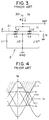
- FIG.3 shows another typical Josephson logic gate that uses a superconducting interferometer loop 2 wherein three Josephson junctions J11, J12 and J13 are included together with superconducting windings La and Lb.
- the input logic signal supplied to the line 21 via an input port A is transferred to the loop 2 as a result of the magnetic coupling of inductances La' and Lb' included in the line 21 with the corresponding superconducting windings La and Lb of the loop 2.
- the bias current I g is supplied from the bias terminal 20 to respective midpoints of the windings La and Lb via the resistor R, and the bias current thus supplied is caused to flow to the superconducting ground plane GND via the Josephson junctions J11, J12 and J13.
- the device shows an operational characteristic as represented in FIG.4. There, the output of the gate is obtained at the node where the resistor R is connected to the superconducting windings La and Lb.
- the region of the finite voltage state of the Josephson junctions J11 - J13 is indicated by the hatching.
- the region of the finite voltage state is expanded as compared with the characteristic curve shown in FIG.2.
- the device of FIG.3 shows an improved operational margin as compared with the device of FIG.1.
- the device of FIG.3 is used successfully to construct the dual input AND gate.
- another input line is provided in magnetic coupling with the interferometer loop 2, and the bias current I g is set such that the transition occurs only when the input current is supplied to both input lines simultaneously.
- the bias current I g is set such that the transition occurs only when the input current is supplied to both input lines simultaneously.
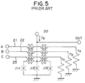
- FIG.5 shows such a three-input Josephson AND gate constructed based upon the superconducting interferometer 2 of FIG.3, wherein there are provided three input lines 21 - 23 respectively connected to input ports A - C.
- the bias current I g is set to a magnitude such that the transition of the Josephson junctions J11 - J13 occurs only when the input current is caused to flow simultaneously through the input lines 21 - 23 in correspondence to the logic state wherein the logic data "1" is supplied simultaneously to the input ports A - C.
- Another and more specific object of the present invention is to provide a Josephson AND gate that is capable of increasing the number of input ports without sacrificing the reliability of operation.
- Another object of the present invention is to provide a multiple-input Josephson AND gate having a plurality of input ports, comprising: a plurality of Josephson logic gate elements provided in number corresponding to a number of said input ports and cascaded with each other from a first stage to a final stage, each of said Josephson logic gate elements of said first through final stages comprising: a superconducting quantum interferometer for producing an output signal in response to a transition from a superconducting state to a finite voltage state; an input line connected to a corresponding input port for carrying thereon an input current, said input line being coupled magnetically to the superconducting quantum interferometer for transferring the input current to said superconducting quantum interferometer; and biasing means for supplying a bias current to said superconducting quantum interferometer, said biasing means supplying the bias current with a level such that said superconducting quantum interferometer causes said transition to the finite voltage stage in response to the input current supplied to the input line, each of said biasing means of said
- the transition of the Josephson gate elements occurs first at the initial stage and proceeds to the final stage consecutively.
- a logic signal indicative of the result of the AND operation is obtained at the Josephson logic gate element of the final stage.
- Another object of the present invention is to provide various Josephson logic circuits that use therein a number of Josephson AND gates each having a plurality of input ports.
- Another object of the present invention is to provide a Josephson decoder circuit for decoding input data represented by a plurality of bits, comprising: a plurality of multiple-input Josephson AND gates each including a plurality of Josephson logic gate elements with a number corresponding to a number of bits of the input data, said plurality of Josephson logic gate elements being cascaded, in each Josephson AND gate, with each other from a first stage to a final stage; each of said Josephson logic gate elements comprising: a superconducting quantum interferometer for producing an output signal in response to a transition from a superconducting state to a finite voltage state; an input line connected to a corresponding input port for carrying thereon an input current, said input line being coupled magnetically to the superconducting quantum interferometer for transferring the input current to said superconducting quantum interferometer; and biasing means for supplying a bias current to said superconducting quantum interferometer, said biasing means supplying the bias current with a level such that said superconducting
- Another object of the present invention is to provide a programmable logic array circuit supplied with input data for producing output data after a predetermined logic operation, comprising: a programmable Josephson AND array comprising a plurality of multiple-input Josephson AND gates each including a plurality of Josephson logic gate elements with a number corresponding to a number of bits of the input data, said plurality of Josephson logic gate elements being cascaded, in each Josephson AND gate, with each other from a first stage to a final stage; each of said Josephson logic gate elements comprising: a superconducting quantum interferometer for producing an output signal in response to a transition from a superconducting state to a finite voltage state; an input line connected to a corresponding input port for carrying thereon an input current, said input line being coupled magnetically to the superconducting quantum interferometer for transferring the input current to said superconducting quantum interferometer; and biasing means for supplying a bias current to said superconducting quantum interferometer, said biasing means supplying the
- FIG.6 shows a four-input AND gate according to a first embodiment of the present invention.
- the circuit includes a first input stage 11, a second input stage 12, a third input stage 13, a fourth input stage 14 and an output stage 15, wherein the first stage 11 includes a superconducting quantum interferometer S1 that has a construction substantially identical with the Josephson gate explained with reference to FIG.3.
- the quantum interferometer S1 is supplied with an a.c. bias current from a bias bus 16 via a resistor Rs1 and operates similarly to the device of FIG.3 with the operational characteristic shown in FIG.4.
- an a.c. current source similar to the a.c. current source 160 is connected to the bias bus 16 for supplying the a.c. bias current thereto.
- the second stage 12 in turn includes a Josephson junction J2 having a first end connected to the output terminal of the device S1 via a resistor R1 and another end connected to the superconducting ground plane.
- the first end of the Josephson junction J2 is connected further to the bias bus 16 via a resistor Rs2 and the bias current is caused to flow to the ground plane as long as the Josephson junction J2 is in the superconducting state.
- the second stage 12 includes a superconducting quantum interferometer S2 that is connected to the first end of the Josephson junction J2 via a resistor R2 for receiving the bias current. As long as the Josephson junction J2 is in the superconducting state, no bias current is supplied to the superconducting interferometer S2, and the superconducting interferometer S2 is held in the superconducting state.
- the third stage 13 and the fourth stage 14 have a construction substantially identical with the construction of the second stage 12.
- the third stage 13 includes a Josephson junction J3 that is biased via a resistor Rs3 at a first end and is connected to the superconducting ground plane at the other end. Further, the first end of the Josephson junction J3 is connected to the output terminal of the superconducting quantum interferometer S2 of the previous stage via a resistor R31, while the same first end of the Josephson junction J3 is connected to a superconducting quantum interferometer S3 via a resistor R32.
- the fourth stage 14 includes a Josephson junctions J4 that is biased via a resistor Rs4 at a first end and is connected to the superconducting ground plane at the other end. Further, the first end of the Josephson junction J4 is connected to the output terminal of the superconducting quantum interferometer S3 of the previous stage via a resistor R41, while the same first end of the Josephson junction J4 is connected to a superconducting quantum interferometer S4 via a resistor R42.
- the stage 13 is connected in cascade to the stage 12 while the stage 14 is connected in cascade to the stage 13.
- a Josephson junction J5 is provided such that the Josephson junction J5 has a first end that is connected to the superconducting quantum interferometer S4 of the previous stage via the resistor R51 and a second end connected to the superconducting ground plane. Further, the bias current is supplied to the Josephson junction J5 via a resistor Rs5. There, a load resistance R L is connected to an output terminal OUT that in turn is connected to the node where the resistors R51 and Rs5 are connected with each other at the first end of the Josephson junction J5.
- the load resistance R L may represent the equivalent load resistance of the Josephson circuits that are connected after the output stage 15.
- the Josephson junctions J11, J12 and J13 are configured such that the critical current of the Josephson junction J12 is twice as large as the critical current of the Josephson junction J11 or the critical current of the Josephson junction J13. There, the Josephson junctions J11 and the Josephson junction J13 have the same critical current. On the other hand, the Josephson junctions J2 - J5 are configured to have a same critical current represented as I m .
- the values of the resistors R22, R32 and R42 are all set equal to V g /I m wherein V g represents the gap voltage of the Josephson junctions J2 - J5. More specifically, the critical current I m may be set equal to 0.4mA, and the value of the resistors R22 - R42 is set to 8 ⁇ . The value of the resistors R21 - R51 may be set to 2 ⁇ .
- the bias current is supplied from the bias bus 16 to each of the superconducting quantum interferometers S1 - S4 as well as to each of the Josephson junctions J2 - J5.
- an input signal A supplied to the first stage causes a transition of the superconducting quantum interferometer S1 and the bias current is supplied from the resistor Rs1 to the Josephson junction J2 via the resistor R21.
- the Josephson junction J2 is driven with a bias current that is a sum of the bias current flowing through the resistor R21 and the resistor Rs2.
- the Josephson junction J2 causes a switching to the finite voltage state. It should be noted that, before the transition of the superconducting quantum interferometer S1, the bias current is not supplied to the Josephson junction J2 via the resistor R21 because of the zero resistance of the superconducting quantum interferometer S1.
- a bias current is supplied from the resistor Rs2 to the superconducting quantum interferometer S2 via the resistor R22. It should be noted that the superconducting quantum interferometer S2 is not biased at all before the Josephson junction J2 switches.
- the superconducting quantum interferometer S2 causes the switching to the finite voltage state and the bias current is now supplied to the Josephson junction J3 via the resistor R31.
- the Josephson junction J3 is biased by a bias current that is equal to the sum of the bias current supplied via the Josephson junction J3 and the bias current supplied via the resistor Rs3.
- the Josephson junction J3 causes a switching to the finite voltage state.
- This switching of the Josephson junction J3 in turn causes the biasing of the superconducting quantum interferometer S3 and the superconducting quantum interferometer S3 is thereby switched to the finite voltage state when there is an input to the input port C.
- the switching of the superconducting interferometer S i and the Josephson junction J i proceeds consecutively from the initial stage to the final stage, provided that an input signal indicating the logic high level is supplied to all of the input ports A - D.
- the suffix i represents the number of the stage.
- the circuit of FIG.6 operates as a multiple-input AND gate.
- the Josephson junctions J2 - J5 produce a voltage corresponding to the gap voltage of the Josephson junction when switched to the finite voltage state.
- the gap voltage is determined by the material that is used for the Josephson junction, this means that the bias current supplied to the superconducting quantum interferometer S i from the preceding Josephson junction J i via the resistor R i2 is determined without ambiguity by the value of the resistor R i2 .
- the bias current that has caused the switching of the superconducting quantum interferometer of the previous stage such as S i-1 does not affect at all the bias current that causes the switching of the superconducting quantum interferometer S i .
- the operation of the multiple-input AND gate of FIG.6 is reliable even when the number of stage is increased in correspondence to the increased number of input ports.
- each superconducting quantum interferometer S i has only one input line. Thereby, one can obtain a sufficient operational margin for the switching operation of the superconducting quantum interferometer. See the operational characteristic of FIG.3. Because of the sufficient operational margin, it is generally not necessary supply input signal to the port A in correspondence to the progressive operation from the first state to the final stage. Even when the input signals are supplied simultaneously to the entire input ports, there is a sufficient margin of time for the foregoing progressive switching operation.
- FIG.7 shows a four-input AND gate according to a second embodiment of the present invention.
- the Josephson junction J2 and the corresponding bias resistance Rs2 is omitted.
- the superconducting quantum interferometer S2 of the second state is supplied with the bias current from the resistors Rs1 and R22 when the superconducting quantum interferometer S1 has caused a switching.
- the foregoing progressive switching occurs and the circuit operates as the multiple-input AND gate.
- the margin of the bias current may become somewhat stringent, the circuit of the present invention has an advantage of reduced number of parts.
- FIG.8 shows a four-input AND gate according to a third embodiment of the present invention.
- the circuit of FIG.8 is substantially identical with the circuit of FIG.6 except that a two-junction type superconducting quantum interferometer S5 as shown in FIG.1 is used in place of the superconducting quantum interferometer S1.
- the superconducting quantum interferometer S5 may be the symmetric type wherein the Josephson junctions J11 and J12 both have the same critical current or the asymmetric type wherein the critical current is different in the Josephson junction J11 and J21.
- the circuit of FIG.8 has an advantageous feature in that the circuit construction can be simplified as a result of use of the two-junction type superconducting quantum interferometer.
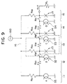
- FIG.9 shows a four-input AND gate according to a fourth embodiment of the present invention.
- the superconducting quantum interferometer S1 of the circuit of FIG.7 is replaced with the two-junction type superconducting quantum interferometer S5.
- the circuit of FIG.9 will be omitted.
- FIG.10 shows a four-input AND gate according to a fifth embodiment of the present invention.
- the superconducting quantum interferometers S1 - S4 of FIG.6 are replaced with two-junction type superconducting quantum interferometers S5 - S8, respectively.
- the two-junction type superconducting quantum interferomters it is possible to simplify the circuit construction and increase the integration density. As other features about the construction and operation are obvious from the description of the previous embodiments, further description of the circuit of FIG.10 will be omitted.
- FIG.11 shows a four-input AND gate according to a sixth embodiment of the present invention.
- the circuit has a construction substantially identical with the circuit of FIG.7 except that the superconducting quantum interferometers S1 - S4 are replaced with the two-junction type superconducting quantum interferometers S5 - S8.
- the circuit of FIG.11 will be omitted.
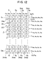
- FIG.12 shows a Josephson decoder circuit according to a seventh embodiment of the present invention wherein the foregoing multiple-input Josephson AND gate is used.
- each Josephson AND gate G i produces an output at an output terminal OUT i in corresponding to a combination of input signals that is different in each Josephson AND gate as indicated in FIG.12.
- the circuit construction can be simplified significantly over the conventional decoder circuit wherein the multiple-input AND gate is constructed by using a number of Josephson AND gates and Josephson OR gates.
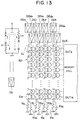
- FIG.13 shows a Josephson decoder circuit according to an eighth embodiment of the present invention, wherein the Josephson decoder circuit has a construction similar to the circuit of FIG.12 except that there are provided voltage boosters DG0 - DG3 and DG 0b - DG 3b in correspondence to each signal line l of the interconnection wiring fixture 30 for boosting the voltage level of the input signals A0 - A3 and A 0b -A 3b .
- the voltage boosters may have a construction proposed previously by the inventor of the present invention and disclosed in the Laid-open European Patent Application EP 0 441 299, which is incorporated herein as reference.
- FIG.13 shows the case wherein the Josephson decoder circuit is used for a memory decoder that addresses a memory cell.
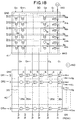
- FIG.14 shows a Josephson decoder circuit according to ninth embodiment of the present invention, wherein the decoder circuit of the present invention has a construction substantially identical with the construction of the decoder of FIG.13 except that voltage boosters EG0 - EG3 and EG 0b - EG 3b are provided in place of the voltage boosters DG0 - EG3 and DG 0b -DG 3b .
- the construction of each voltage booster EG is represented also in FIG.14. More detailed description of the voltage booster EG can be found in the aforementioned Laid-open European Patent Application EP 0 411 299. Thereby, one can improve the operational speed of the decoding operation similarly to the previous embodiment.
- the Josephson memory decoder of the present embodiment has a construction similar to the Josephson decoder of FIG.12 except that each output of the Josephson AND gate G i is provided with a fuse f i that is selectively blown up by irradiation of a laser beam.
- the Josephson memory decoder of FIG.15(A) includes a redundant gate G red having a similar construction as other Josephson AND gates, for addressing a redundant memory cell.
- the redundant gate G red is connected to the interconnection wiring fixture 30 via programmable wiring elements 31, 32 of which construction is shown in derail in FIG.15(B).
- the programmable wiring element includes conductor strips 30a and 30b that extend as a part of the signal line l of the interconnection wiring fixture 30.
- crossing conductor strips 30c that cross with each other between the conductor strips 30a and 30b.
- the crossing conductor strips 30c are disconnected by irradiation of the laser beam.
- the fuse f r at the output of the redundant gate G red is disconnected simultaneously. Thereby, the addressing of the memory cell by the redundant gate G red is prohibited and the Josephson memory decoder of FIG.15(A) operates similarly to the Josephson decoder of FIG.12.
- the fuse for the Josephson AND gate that addresses the defective memory cell such as the gate G4 is disconnected by the laser beam irradiation, and the programmable wiring elements 31 and 32 are modified as shown in FIGS.16(B) and 16(C) also by the laser beam irradiation.
- the elements designated by Y is modified as shown in FIG.16(B) by blowing up the conductor strips 30a and 30b.
- the true input signal A0 and the complementary input signal A 0b are exchanged.
- the gate G4 a similar exchange of the true input signal and the complementary input signal is achieved also for the signals A1 and A 1b .
- the crossing conductor strips 30c are blown up by the irradiation of the laser beam. Thereby, the true input signal and the complementary input signal are passed through the programmable wiring element 31 as they are, without being exchanged.
- the redundant Josephson AND gate G red is activated by the combination of the logic state of the input signals that is identical with the combination that activates the Josephson AND gate G4. Thereby, the redundant memory cell is addressed by the redundant Josephson AND gate G red . On the other hand, the selection of the defective memory cell is prohibited by disconnecting the fuse f4 simultaneously.
- another programmable wiring element 32 that is programmed such that the exchange of the true input signal and the complementary input signal caused by the programmable wiring element 31 is canceled upon passage of the input signals therethrough.
- the programmable wiring element 32 for the input signals A0 and A 0b are programmed identically with the element 31 as shown in FIG.16(B) such that the input signals A0 and A 0b are exchanged again.
- a similar programming is made also for the programmable wiring element 32 for the input signals A1 and A 1b .
- the programmable wiring element 32 for the input signals A2 and A 2b , A3 and A 3b are programmed as shown in FIG.16(C) in correspondence to the programming of the corresponding element 31.
- the programmable wiring elements 31 and 32 are provided as a pair in each signal line l of the interconnection wiring fixture 30, one can achieve the supply of the input signals to each of the normal Josephson AND gates G1 - G n as if there is no redundant Josephson AND gate G red .
- FIG.17 shows the case wherein two redundant Josephson AND gates G red1 and G red2 are provided.
- the programmable wiring elements 31, 32 and 33 are provided as indicated in the drawing.
- FIG.17 shows the case wherein two redundant Josephson AND gates G red1 and G red2 are provided.
- the programmable wiring elements 31, 32 and 33 are provided as indicated in the drawing.
- FIG.17 shows the case wherein two redundant Josephson AND gates G red1 and G red2 are provided.
- the programmable wiring elements 31, 32 and 33 are provided as indicated in the drawing.
- FIG.18 shows a twelfth embodiment of the present invention.
- the circuit of the present invention forms a programmable logic array and includes an AND array 41 and an OR array 42, wherein the AND array 41 has a construction similar to the decoder of FIG.12 in that there are provided a plurality of Josephson AND gates G1 - G n connected with each other by the interconnection wiring fixture 30.
- the AND array 41 is different from the decoder of FIG.12 in that some of the superconducting quantum interferometers in the Josephson AND gate represented as S x are de-coupled from the signal line l of the interconnection wiring fixture 30. Such a decoupling can be achieved by providing a conductor path such that the signal line l circumvents some of the superconducting quantum interferometers.
- the AND array 41 produces output signals O1 - O n with a number corresponding to the number of the Josephson AND gates arranged in the AND array 41.
- the logic product operation is achieved based upon the input signals A0 . . . except for those input signals that are supplied without magnetic coupling with the superconducting quantum interferomters.
- the OR array 42 includes a number of OR gates OR1 - OR m , wherein each OR gate includes a number of superconducting quantum interferometers S connected in series for receiving the a.c. bias current from the a.c. current source 160. It should be noted that the a.c. current source 160 also drives the superconducting quantum interferometers of the Josephson AND gate G1 - G n . As the superconducting quantum interferometers S are connected in series between the a.c. current source 160 and the superconducting ground plane GND, the switching of any one of the superconducting quantum interferometer S causes a transition of the output voltage obtained at an output terminal X0 - X m . In other words, the gate OR1 - OR m achieves the logic OR operation.
- the signals OR1 - OR m are transferred from one OR gate to the next OR gate along the signal lines 351 - 35 n of an interconnection wiring fixture 35 that is similar to the interconnection wiring fixture 30.
- the signals O1 - O n cause the switching of the OR array 42.
- some of the signal lines 351 - 35 n are provided to bypass the superconducting quantum interferometer of the OR gates such that the signal that is supplied on the signal line does not cause the switching of the OR gate.
- FIG.19 shows a programmable logic array according to a thirteenth embodiment of the present invention.
- the programmable logic array includes an AND array 51 substantially identical in construction with the AND array 41 of the previous embodiment and an OR array 52 to be described below.
- the AND array 51 produces the output signals O1 - O n in response to the input signals A0, A 0b , . . . and supplies the same to the OR array 52.
- the OR array 52 includes a number of Josephson OR gates each having a construction shown in FIG.20 and achieves the logic OR operation similarly to the OR array 42. Thereby, the result of the desired logic operation is obtained at output terminals X0 - X m .
- FIG.20 shows the construction of the Josephson OR gate used in the OR array 52.
- the Josephson OR gate has a construction similar to the Josephson AND gate described with reference to FIG.6, except that there is provided an additional resistance Rs i ' in correspondence to each superconducting quantum interferometer S i of the i-th stage for supplying thereto an a.c. bias current from the bias bus 16. There, each superconducting quantum interferometer S i is biased by the resistor Rs i ' to a level slightly below a level above which the transition to the finite voltage state occurs.
- the input signal to the superconducting quantum interferometer of any stage causes the switching of the superconducting quantum interferometer to the finite voltage stage, and such a transition to the finite voltage state triggers the progressive transition of the superconducting quantum interferomters of the subsequent stages as described already with reference to the Josephson AND gate.
- the circuit of FIG.20 acts as the logic OR gate.
Landscapes
- Physics & Mathematics (AREA)
- Mathematical Physics (AREA)
- Engineering & Computer Science (AREA)
- Computer Hardware Design (AREA)
- Computing Systems (AREA)
- General Engineering & Computer Science (AREA)
- Theoretical Computer Science (AREA)
- Superconductor Devices And Manufacturing Methods Thereof (AREA)
- Logic Circuits (AREA)
Applications Claiming Priority (6)
| Application Number | Priority Date | Filing Date | Title |
|---|---|---|---|
| JP60450/91 | 1991-03-25 | ||
| JP6045091 | 1991-03-25 | ||
| JP23035291 | 1991-09-10 | ||
| JP230352/91 | 1991-09-10 | ||
| JP237849/91 | 1991-09-18 | ||
| JP23784991 | 1991-09-18 |
Publications (3)
| Publication Number | Publication Date |
|---|---|
| EP0506345A2 true EP0506345A2 (de) | 1992-09-30 |
| EP0506345A3 EP0506345A3 (en) | 1993-02-10 |
| EP0506345B1 EP0506345B1 (de) | 1997-01-15 |
Family
ID=27297194
Family Applications (1)
| Application Number | Title | Priority Date | Filing Date |
|---|---|---|---|
| EP92302541A Expired - Lifetime EP0506345B1 (de) | 1991-03-25 | 1992-03-25 | Josephson Gatter mit einer Vielzahl von Eingangstoren und Josephson Schaltung mit solchem Gatter |
Country Status (3)
| Country | Link |
|---|---|
| US (1) | US5233244A (de) |
| EP (1) | EP0506345B1 (de) |
| DE (1) | DE69216669T2 (de) |
Cited By (3)
| Publication number | Priority date | Publication date | Assignee | Title |
|---|---|---|---|---|
| WO1997002661A1 (en) * | 1995-06-30 | 1997-01-23 | Telefonaktiebolaget Lm Ericsson (Publ) | Arrangement and method relating to digital information |
| US11750189B2 (en) | 2020-12-24 | 2023-09-05 | International Business Machines Corporation | Programmable and reprogrammable quantum circuit |
| US20240038298A1 (en) * | 2022-07-27 | 2024-02-01 | Imec Vzw | Josephson Static Random Access Memory |
Families Citing this family (8)
| Publication number | Priority date | Publication date | Assignee | Title |
|---|---|---|---|---|
| US6154044A (en) | 1998-11-20 | 2000-11-28 | Trw Inc. | Superconductive logic gate and random access memory |
| JP2971066B1 (ja) * | 1998-12-02 | 1999-11-02 | 株式会社日立製作所 | 超電導単一磁束量子論理回路 |
| US6734699B1 (en) * | 1999-07-14 | 2004-05-11 | Northrop Grumman Corporation | Self-clocked complementary logic |
| US6549059B1 (en) * | 2001-02-23 | 2003-04-15 | Trw Inc. | Underdamped Josephson transmission line |
| US6518786B2 (en) | 2001-06-15 | 2003-02-11 | Trw Inc. | Combinational logic using asynchronous single-flux quantum gates |
| GB2457706B (en) * | 2008-02-22 | 2010-03-10 | Siemens Magnet Technology Ltd | Coil energisation apparatus and method of energising a superconductive coil |
| US8571614B1 (en) | 2009-10-12 | 2013-10-29 | Hypres, Inc. | Low-power biasing networks for superconducting integrated circuits |
| US10222416B1 (en) | 2015-04-14 | 2019-03-05 | Hypres, Inc. | System and method for array diagnostics in superconducting integrated circuit |
Family Cites Families (14)
| Publication number | Priority date | Publication date | Assignee | Title |
|---|---|---|---|---|
| CH578290A5 (de) * | 1972-11-17 | 1976-07-30 | Ibm | |
| US3848259A (en) * | 1973-10-30 | 1974-11-12 | Ibm | Multicontrol logic gate design |
| US4039856A (en) * | 1975-12-02 | 1977-08-02 | International Business Machines Corporation | Distributed josephson junction logic circuit |
| US4097265A (en) | 1975-12-30 | 1978-06-27 | Chevron Research Company | 3,5-Dimethyl-2-thienylcarboxanilide and 3,5-dimethyl-2-thienyl-(N-haloalkylthiocarboxanilide) herbicides |
| US4097765A (en) * | 1976-06-30 | 1978-06-27 | International Business Machines Corporation | Electronically alterable non-latching Josephson AND, OR, NAND, NOR logic circuit |
| US4274015A (en) * | 1978-12-29 | 1981-06-16 | International Business Machines Corporation | Self-resetting Josephson digital current amplifier |
| US4275314A (en) * | 1979-04-30 | 1981-06-23 | Bell Telephone Laboratories, Incorporated | Josephson Atto-Weber switch |
| DE3276990D1 (en) * | 1981-03-31 | 1987-09-17 | Fujitsu Ltd | Josephson-junction logic circuit |
| US4413196A (en) * | 1981-08-31 | 1983-11-01 | Sperry Corporation | Three Josephson junction direct coupled isolation circuit |
| US4413197A (en) * | 1981-08-31 | 1983-11-01 | Sperry Corporation | Four Josephson junction direct-coupled and gate circuit |
| JPS59183530A (ja) * | 1983-04-02 | 1984-10-18 | Nippon Telegr & Teleph Corp <Ntt> | 超伝導ゲ−ト回路 |
| JPH01233915A (ja) * | 1988-03-15 | 1989-09-19 | Fujitsu Ltd | 超伝導論理回路 |
| JPH0824258B2 (ja) * | 1989-06-09 | 1996-03-06 | 株式会社日立製作所 | 超電導論理回路素子 |
| US5164618A (en) * | 1991-08-14 | 1992-11-17 | Westinghouse Electric Corp. | Superconducting gate array cells |
-
1992
- 1992-03-24 US US07/856,730 patent/US5233244A/en not_active Expired - Fee Related
- 1992-03-25 EP EP92302541A patent/EP0506345B1/de not_active Expired - Lifetime
- 1992-03-25 DE DE69216669T patent/DE69216669T2/de not_active Expired - Fee Related
Cited By (5)
| Publication number | Priority date | Publication date | Assignee | Title |
|---|---|---|---|---|
| WO1997002661A1 (en) * | 1995-06-30 | 1997-01-23 | Telefonaktiebolaget Lm Ericsson (Publ) | Arrangement and method relating to digital information |
| CN1101083C (zh) * | 1995-06-30 | 2003-02-05 | 艾利森电话股份有限公司 | 一种涉及数字信息的装置和方法 |
| US11750189B2 (en) | 2020-12-24 | 2023-09-05 | International Business Machines Corporation | Programmable and reprogrammable quantum circuit |
| US12418290B2 (en) | 2020-12-24 | 2025-09-16 | International Business Machines Corporation | Programmable and reprogrammable quantum circuit |
| US20240038298A1 (en) * | 2022-07-27 | 2024-02-01 | Imec Vzw | Josephson Static Random Access Memory |
Also Published As
| Publication number | Publication date |
|---|---|
| US5233244A (en) | 1993-08-03 |
| EP0506345A3 (en) | 1993-02-10 |
| DE69216669D1 (de) | 1997-02-27 |
| EP0506345B1 (de) | 1997-01-15 |
| DE69216669T2 (de) | 1997-05-07 |
Similar Documents
| Publication | Publication Date | Title |
|---|---|---|
| CA3101348C (en) | Jtl-based superconducting logic arrays and fpgas | |
| EP0506345A2 (de) | Josephson Gatter mit einer Vielzahl von Eingangstoren und Josephson Schaltung mit solchem Gatter | |
| WO1985003394A1 (en) | Programmable array logic circuit with shared product terms | |
| EP0366530B1 (de) | Josephson-Speicherschaltung | |
| US4482821A (en) | Superconductive logic circuit | |
| EP0048115B1 (de) | Decodierschaltung, wobei Josephson-Elemente verwendet werden | |
| US5164618A (en) | Superconducting gate array cells | |
| US4555643A (en) | Superconducting logic circuit and superconducting switching device therefor | |
| EP0138126A2 (de) | Logische Schaltung mit Niedrigstromstruktur | |
| JPH05136689A (ja) | 多入力ジヨセフソンandゲート、多入力ジヨセフソンorゲート、ジヨセフソンデコーダ回路、及びジヨセフソンpla回路 | |
| EP0813304B1 (de) | Symmetrische Auswahlschaltung für Ereignislogik | |
| JP2924398B2 (ja) | ジョセフソン極性切換型駆動回路 | |
| US7307295B2 (en) | Method and an apparatus for a hard-coded bit value changeable in any layer of metal | |
| CA1201529A (en) | Superconducting read-only memories or programable logic arrays having the same | |
| JPH0226417B2 (de) | ||
| JPH0563554A (ja) | 超伝導集積回路 | |
| JPH0772995B2 (ja) | 超伝導記憶回路 | |
| Yuh | A wide-margin, multiple-fan-in NOR gate for Josephson decoder | |
| JPS58147235A (ja) | 超伝導選択回路 | |
| JPH0411956B2 (de) | ||
| JPH02254698A (ja) | 極性切換型ジョセフソン駆動回路 | |
| JPH0411955B2 (de) | ||
| JPH01195723A (ja) | デコーダ回路 | |
| JPS61262321A (ja) | ジヨセフソン抵抗結合型否定回路 | |
| JPH0368478B2 (de) |
Legal Events
| Date | Code | Title | Description |
|---|---|---|---|
| PUAI | Public reference made under article 153(3) epc to a published international application that has entered the european phase |
Free format text: ORIGINAL CODE: 0009012 |
|
| AK | Designated contracting states |
Kind code of ref document: A2 Designated state(s): DE FR GB |
|
| PUAL | Search report despatched |
Free format text: ORIGINAL CODE: 0009013 |
|
| AK | Designated contracting states |
Kind code of ref document: A3 Designated state(s): DE FR GB |
|
| 17P | Request for examination filed |
Effective date: 19930408 |
|
| GRAG | Despatch of communication of intention to grant |
Free format text: ORIGINAL CODE: EPIDOS AGRA |
|
| 17Q | First examination report despatched |
Effective date: 19960508 |
|
| GRAH | Despatch of communication of intention to grant a patent |
Free format text: ORIGINAL CODE: EPIDOS IGRA |
|
| GRAH | Despatch of communication of intention to grant a patent |
Free format text: ORIGINAL CODE: EPIDOS IGRA |
|
| GRAA | (expected) grant |
Free format text: ORIGINAL CODE: 0009210 |
|
| AK | Designated contracting states |
Kind code of ref document: B1 Designated state(s): DE FR GB |
|
| REF | Corresponds to: |
Ref document number: 69216669 Country of ref document: DE Date of ref document: 19970227 |
|
| ET | Fr: translation filed | ||
| PLBE | No opposition filed within time limit |
Free format text: ORIGINAL CODE: 0009261 |
|
| STAA | Information on the status of an ep patent application or granted ep patent |
Free format text: STATUS: NO OPPOSITION FILED WITHIN TIME LIMIT |
|
| 26N | No opposition filed | ||
| PGFP | Annual fee paid to national office [announced via postgrant information from national office to epo] |
Ref country code: FR Payment date: 19980310 Year of fee payment: 7 |
|
| PGFP | Annual fee paid to national office [announced via postgrant information from national office to epo] |
Ref country code: GB Payment date: 19980316 Year of fee payment: 7 |
|
| PGFP | Annual fee paid to national office [announced via postgrant information from national office to epo] |
Ref country code: DE Payment date: 19980403 Year of fee payment: 7 |
|
| PG25 | Lapsed in a contracting state [announced via postgrant information from national office to epo] |
Ref country code: GB Free format text: LAPSE BECAUSE OF NON-PAYMENT OF DUE FEES Effective date: 19990325 |
|
| GBPC | Gb: european patent ceased through non-payment of renewal fee |
Effective date: 19990325 |
|
| PG25 | Lapsed in a contracting state [announced via postgrant information from national office to epo] |
Ref country code: FR Free format text: LAPSE BECAUSE OF NON-PAYMENT OF DUE FEES Effective date: 19991130 |
|
| REG | Reference to a national code |
Ref country code: FR Ref legal event code: ST |
|
| PG25 | Lapsed in a contracting state [announced via postgrant information from national office to epo] |
Ref country code: DE Free format text: LAPSE BECAUSE OF NON-PAYMENT OF DUE FEES Effective date: 20000101 |