EP0506362A2 - Bobine - Google Patents
Bobine Download PDFInfo
- Publication number
- EP0506362A2 EP0506362A2 EP92302568A EP92302568A EP0506362A2 EP 0506362 A2 EP0506362 A2 EP 0506362A2 EP 92302568 A EP92302568 A EP 92302568A EP 92302568 A EP92302568 A EP 92302568A EP 0506362 A2 EP0506362 A2 EP 0506362A2
- Authority
- EP
- European Patent Office
- Prior art keywords
- conductor
- coil
- conductors
- insulator
- coil element
- Prior art date
- Legal status (The legal status is an assumption and is not a legal conclusion. Google has not performed a legal analysis and makes no representation as to the accuracy of the status listed.)
- Withdrawn
Links
Images


Classifications
-
- H—ELECTRICITY
- H01—ELECTRIC ELEMENTS
- H01F—MAGNETS; INDUCTANCES; TRANSFORMERS; SELECTION OF MATERIALS FOR THEIR MAGNETIC PROPERTIES
- H01F27/00—Details of transformers or inductances, in general
- H01F27/28—Coils; Windings; Conductive connections
- H01F27/2804—Printed windings
-
- H—ELECTRICITY
- H01—ELECTRIC ELEMENTS
- H01F—MAGNETS; INDUCTANCES; TRANSFORMERS; SELECTION OF MATERIALS FOR THEIR MAGNETIC PROPERTIES
- H01F27/00—Details of transformers or inductances, in general
- H01F27/28—Coils; Windings; Conductive connections
- H01F27/2804—Printed windings
- H01F2027/2809—Printed windings on stacked layers
Definitions
- the present invention relates to coils, and more particularly to coils are usable as electronic parts, for example, in transformers, noise filters, oscillators, etc. or as circuit components of electronic parts.
- Such coils heretofore known comprise a thin conductor which is wound spirally by a machine.
- the coils known in the art have the problem of being large in height per unit number of turns of conductor. This problem becomes more serious when such coils are mounted on printed circuit boards because they fail to assure the circuit board of a high packing density.
- coils have found wide use as electronic parts, they still remain to be reduced in thickness.
- the conventional construction of coils is not suited to the production of a wide variety of coils in small lots and is liable to permit a break of the conductor or damage to the insulation coating when the conductor is wound.
- the conventional coils therefore have problems also with respect to reliability and yield.
- An object of the invention is to porivde a coil having a reduced thickness and suited to produce in many different types in small lots with improved reliability and in a higher yield.
- Another object of the invention is to provide a coil which has a readily controllable number of turns of conductor.
- the present invention provides a coil comprising a plurality of stacked coil elements connected together at conductor ends to form at one series of spiral conductors, each of the coil elements including a sheet insulator, a first conductor in a planar spiral form and provided on one surface of the insulator and a second conductor in a planar spiral form and provided on the other surface of the insulator, the conductors on the respective surfaces of the insulator being wound spirally in directions opposite to each other when seen from above at the same side of the insulator.
- the invention provides a coil comprising at least one coil element, the coil element including a sheet insulator, and a first conductor and a second conductor provided on the insulator and each in a planar spiral form.
- the first conductor and the second conductor are provided on one surface of the sheet insulator, with one of the conductors extending between the turns of the other conductor.
- the first conductor is provided on one surface of the sheet insulator, and the second conductor is disposed on the other surface of the insulator. In either case, the first and second conductors form separate circuits.
- the invention provides a coil comprising stacked coil elements of two different types selected from a first-type coil element, a second-type coil element, a third-type coil element and a fourth-type coil element, the first-type coil element comprising a first conductor and a second conductor provided on at least one surface of a sheet insulator and each in a planar spiral form, one of the first and second conductors extending between turns of the other conductor, the second-type coil element comprising a first conductor and a second conductor provided on at least one surface of a sheet insulator and each in a planar spiral form, one of the first and second conductors of the second-type coil element extending between turns of the other conductor, the conductors of the second-type coil element being spirally wound in one direction opposite to the winding direction of the conductors of the first-type coil element when seen from above at the same side of the insulators, the third-type coil element comprising a conductor in a
- the winding direction of spiral conductors on the front or rear surface of a particular insulator is specified to form a required number of desired series circuits of spiral conductors by coil elements of the invention.
- the coil element of the invention comprises an insulator in the form of a sheet, and at least one conductor in a planar spiral form and provided on one or each surface of the insulator, and is in the form of a sheet in its entirety.
- the coil element will sometimes be referred to as a "coil sheet.”
- a plurality of such coil elements can be assembled or arranged in layers to form at least one series of spiral conductors or two-terminal series circuit. According to the invention, therefore, the assembly of coil elements can be reduced in height, i.e., in thickness, per unit number of turns of conductor. Therefore, the two-terminal series circuit can be provided by a desired number of turns of conductors using a selected number of coil elements having the same number of turns.
- the coil element or coil sheet can be prepared by the same method as printed circuit boards, so that coil sheets which are different in the number of turns can be produced readily.
- the coil sheet has a spiral conductor on each of its front and rear surfaces, these conductors are spirally wound in directions opposite to each other when seen from above at the same side of the sheet.
- a plurality of coil sheets can be made identical in circuit pattern except the external or internal connection of the conductor ends.
- the connections for the ends of front and rear conductors of coil sheets can also be standardized.
- the connections for the conductor inner ends can be established via through holes in the sheets which holes are positioned in phase.
- the interconnections between conductor ends corresponding to intermediate terminals of the two-terminl series circuit can also be standardized.
- conductor outer ends can be interconnected by pads which are positioned in phase.
- the external terminal of the circuit for example, the outer end of the outermost conductor, may be connected to a through hole terminal.
- the transformer can be fabricated using two kinds of coil sheets which are different in circuit pattern.
- the transformer can be obtained using coil sheets of three different circuit patterns, or of two different circuit patterns depending on the position of through holes.
- the present invention is suited to the production of many different types of coils in small lots.
- coils can be fabricated in the same manner as the circuit pattern of printed circuit board, and the conductor need not be coiled in the conventional manner. For this reason, coils can be produced with improved reliability in a high yield without the likelihood of a break in the conductor or damage to the insulation coating.
- the desired product or assembly of coils can be made to have a readily controlled number of turns of conductors by preparing coil sheets having the same number of turns and varying the number of such coil sheet to be used. This ensures a great advantage when coil sheets of the invention are used for fabricating transformers or like devices having two types of windings.
- the construction of the coil of the present invention is usable for the transmission of data in an insulated state in place of the wiring between a computer and a keyboard or the wiring between primary substrates.
- the sheet insulator may be internally provided with a spiral conductor like the one provided on the outer surface thereof.
- the coil sheet 1 comprises an insulator 2 in the form of a sheet, and a first conductor 3-1 and a second conductor 3-2 which are provided on the front surface and the rear surface of the insulator 2, respectively, and each of which is in a planar spiral form.
- the conductors 3 on the respective surfaces are wound spirally in directions opposite to each other when seen from above at the same side of the insulator 2.
- the embodiment shown in FIG. 1 includes a plurality of coil sheets 1 which are in the form of an assembly comprising a two-terminal series circuit serving as a primary winding I, and two-terminal series circuits serving as secondary windings II.
- Each of these two-terminal series circuits comprises two or three coil sheets 1 which are stacked up in layers.
- the front and rear spiral conductors 3 of each coil sheet 1 have inner ends which are connected together at a plated through hole 4 in the center of the sheet.
- the other end, i.e., outer end, of each conductor 3 is connected to the plating of a plated through hole 5 formed at a corner of the coil sheet 1 as a terminal.
- the outer end of each conductor 3 is connected to a pad 6 formed on a required portion of the coil sheet 1.
- the pads 6 of the adjacent coil sheets 1 in each series circuit are joined to each other.
- FIG. 1 comprises one primary winding I and two secondary windings II and is symbolically shown in FIG. 11.
- the two secondary windings II are each in the form of a series circuit formed by two or three coil sheets 1 which are connected together in series.
- the conductor ends corresponding to the external terminals of the series circuit are connected to the platings of the respective plated through holes 5 in corners of the corresponding coil sheets 1 which corners are different in position.
- the two series circuits, i.e., the two secondary windings II are also different in the position of the through holes 5 at which each of such external conductor ends is located.
- FIG. 1 With the embodiment of FIG. 1, seven coil sheets 1 are used to form the specified number of two-terminal series circuits.
- the front and rear circuit patterns of these seven coil sheets 1 can be those shown in FIGS. 2 to 7.
- the first to seventh coil sheets as arranged from above downward in FIG. 1 are indicated at 1-1, 1-2, 1-3, 1-4, 1-5, 1-6 and 1-7, respectively.
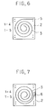
- FIGS. 2, 4 and 6 show the front circuit patterns
- FIGS. 3, 5 and 7 show the rear circuit patterns as seen from the front side of the coil sheet 1.
- FIGS. 1 to 7 reveal that in the case where the assembly of one primary winding and two secondary windings are formed by seven coil sheets, the first, third, sixth and seventh coil sheets, as well as the fourth and fifth coil sheets, can be identical in circuit pattern inclusive of the intermediate and external terminal connections of the series circuit.
- the whole assembly can be formed by coil sheets of three different circuit patterns.
- the third and seventh coil sheets are identical with the first coil sheet as turned upside down, and the fifth coil sheet with the fourth coil sheet as turned upside down.
- the coil sheets to be used can be of two kinds of circuit patterns.
- An assembly comprising one primary winding and one secondary winding can be formed by coil sheets of two different circuit patterns.
- the coil sheets 1 are arranged in layers to form the specified two-terminal series circuits and mounted on a ferrite or like core 7 to make a transformer.
- the coil sheets 1 comprise insulators 2 having holes through which the legs of the core 7 are inserted
- the coil of the invention can be mounted between a printed circuit board and another printed circuit board.
- This type of embodiment is the same as the embodiment of FIG. 36 to be described later in respect of the other type of coil sheet according to this invention as shown in FIG. 12 et. seq.
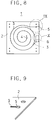
- FIGS. 12, 13 and 14 show an embodiment wherein a coil sheet 1 comprises a first conductor 3-1 and a second conductor 3-2 which are wound spirally on the front surface of an insulator 2 in the form of a sheet and each form a two-terminal circuit.
- One of the conductors extends between the turns of the other conductor.
- the inner ends of the first and second conductors 3-1 and 3-2 are connected by the platings of plated through holes 4′ and 5′ to external conduction lines 40 and 50 (FIG. 14) on the rear surface of the coil sheet 1, respectively.
- the outer ends of the conductors extend into external conduction lines 40, 50 on the front surface of the coil sheet 1, respectively.
- the circuit assembly of the first and second conductors 3-1, 3-2 is shown in FIG.
- the external conduction lines 40, 50 on the rear surface are shown as they are seen from the front side of the coil sheet 1.
- the first and second conductors 3-1, 3-2 are represented by a thick line and a thin line, respectively, for clarity as is the case with the following embodiments.
- the embodiment of FIGS. 12, 13 and 14 comprises coil elements which are not connected in series, that is, the first and second conductors 3-1, 3-2 form separate circuits.
- FIG. 13 shows the combined pattern of the first and second conductors according to this modification and also shows the circuit pattern on the front surface of the embodiment of FIG. 12.
- FIGS. 15, 16 and 17 show another embodiment comprising a first-type coil sheet 1 (FIG. 16) and a second-type coil sheet 1 (FIG. 17) in combination.
- the first-type coil sheet 1 comprises a first conductor 3-1 and a second conductor 3-2 which are spirally wound on the front surface of a sheet insulator 2 and one of which extends between the turns of the other conductor.
- the second-type coil sheet 1 comprises first and second conductors and has substantially the same construction as the first-type coil sheet except that these conductors are spirally wound in a direction opposite to the direction of winding of the conductors on the first-type coil sheet.
- the coil sheets of the two types may be so formed that the single sheet insulator 2 having the first and second conductors 3-1, 3-2 of one type on one surface thereof is provided on the other surface thereof with the first and second conductors 3-1, 3-2 of the other type.
- the two sheet insulators 2 each provided with the first and second conductors 3-1, 3-2 on one surface thereof as specified may be superposed.
- the first and second conductors 3-1, 3-2 on each of the upper and lower sheet insulators 2 may be positioned on an outer surface or inside the assembly
- the inner ends of the first and second conductors 3-1, 3-2 on the front side are connected by the platings of plated through holes 4′, 5′ to the inner ends of the first and second conductors 3-1, 3-2 on the rear side, respectively.
- the outer ends of the conductors on each side extend into external conduction lines 40, 50 on the same side.
- the overall circuit construction of the four first and second conductors 3-1, 3-2 is shown in FIG. 15 in the same manner as in FIG. 12.
- the first and second conductors on the rear side (FIG. 17) are shown as they are seen from the front side of the coil sheet 1.
- the two first conductors 3-1, as well as the two second conductors 3-2, of the embodiment of FIGS. 15 to 17 form a two-terminal series circuit.
- Such coil sheets are assembled or stacked up to provide specified circuits.
- FIGS. 18, 19, 20 and 21 show an embodiment comprising two types of coil sheets in combination, i.e., a third-type coil sheet 1 (FIG. 19) having a planar spiral conductor 3 formed on the front surface of a sheet insulator 2, and a fourth-type coil sheet 1 (FIG. 21) having substantially the same construction as the third-type coil sheet except that the conductor is spirally wound in a direction opposite to the winding direction of the conductor of the third-type coil sheet when seen from above at the same side of the insulators 2.
- a third-type coil sheet 1 FIG. 19
- a fourth-type coil sheet 1 FIG. 21
- FIGS. 18 to 21 has a three-layer construction wherein the coil sheet 1 (FIG. 19) of one of the third and fourth types is the upper-layer, a sheet insulator 21 (FIG. 20) having external conduction lines 40, 50 on its front surface is the intermediate layer, and the coil sheet 1 (FIG. 21) of the other type is the lower layer.
- the inner end of the conductor 3 of the upper coil sheet 1 is connected by the plating of a plated through hole 4′ to the external conduction line 40 on the sheet insulator 21 as the intermediate layer, and the outer end thereof is connected to an external conduction line on the upper layer.
- the inner end of the conductor 3 of the lower coil sheet 1 is connected by the plating of a plated through hole 5′ to the external conduction line 50 on the sheet insulator 21 as the intermediate layer, and the outer end thereof extends into an external conduction line on the lower layer.
- the overall circuit construction of these coil sheets is shown in FIG. 18 in the same manner as the foregoing embodiments.
- the conduction lines 40, 50 on the intermediate layer and the conductors 3 on the lower layer are illustrated as they are seen from the front side of the upper layer.
- the conductor 3 of one of the two coil sheets 1 of the embodiment shown in FIGS. 18 to 21 corresponds to the first conductor 3-1 of the embodiments of FIGS. 12 to 17, and the conductor 3 of the other coil sheet to the second conductor 3-2 thereof.
- Each of these conductors provides a two terminal circuit.
- Such coil sheets of the embodiment of FIGS.18 to 21 are assembled or stacked up to form specified circuits.
- FIGS. 22, 23 and 24 show an embodiment of modified three-layer construction.
- an upper-layer coil sheet 1 (FIG. 22) and an intermediate-layer coil sheet 1 (FIG. 23) each comprise a planar spiral conductor 3 on a sheet insulator 2 and have substantially the same construction except that the conductors 3 on these sheets 1 are spirally wound in directions opposite to each other when seen from above at the same side of the insulators 2.
- a lower-layer coil sheet 1 (FIG. 24) is substantially the same as the upper-layer coil sheet 1.
- the coil sheets of the upper and lower layers are those of the third type, while the intermediate-layer coil sheet is of the fourth type.
- the inner end of the conductor 3 of the upper-layer coil sheet 1 is connected by the plating of a plated through hole 4′ to the inner end of the conductor 3 of the intermediate-layer coil sheet, and the outer ends of these conductors 3 are each connected to an external conduction line 40 on the surface of the corresponding layer.
- the inner end of the conductor 3 of the lower-layer coil sheet 1 is connected by the plating of a plated through hole 5′ to an external conduction line 50 on the surface of the insulator 2 of the same sheet opposite to the conductor-bearing surface thereof.
- the outer end of the same conductor 3 extends into an external conduction line 50 on the latter surface.
- the conductors of the intermediate and lower layers are shown as they are seen from the front side of the upper layer.
- the external conduction line of the conductor inner end of the lower-layer coil sheet 1 shown in FIG. 24 and the external conduction line of the conductor outer end thereof are arranged on the respective different surfaces of the insulator 2 as stated above, while this lower-layer coil sheet is shown as seen from the front side of the upper layer, so that the external conduction line of the conductor inner end is indicated in a broken line for clarity.
- the conductors 3 of the upper and intermediate layers correspond to the aforementioned first conductor 3-1, and the conductor 3 of the lower layer to the second conductor 3-2.
- the former two conductors 3 form a two-terminal series circuit, and the other conductor forms a two-terminal circuit.
- the embodiment of this type is also an example of combination of two types, i.e., the third-type coil sheet and the fourth-type coil sheet.
- Such coil sheets of the embodiment of FIGS. 22, 23 and 24 are assembled or stacked up to form specified circuits.
- FIGS. 25, 26 and 27 show another modification of three-layer construction.
- an upper-layer coil sheet 1 (FIG. 25) forms a two-terminai circuit
- intermediate-layer and lower-layer coil sheets 1 (FIGS. 26 and 27) provide a two-terminal series circuit.
- External conduction lines 40 and 50 are so arranged as to form these circuits.
- the modification has substantially the same construction as the modified embodiment of FIGS. 22 to 24.
- the conductor 3 of the upper-layer coil sheet 1 corresponds to the first conductor 3-1
- the conductors 3 of the intermediate-layer and lower-layer coil sheets 1 correspond to the second conductor 3-2.
- the external conduction line of the conductor inner end of the upper-layer coil sheet 1 is indicated in a broken line as in FIG. 24.
- the upper-layer and lower-layer coil sheets are those of the third type, and the intermediate layer coil sheet is of the fourth type.
- Such coil sheets of the modification of FIGS. 25 to 27 are assembled or stacked up to form specified circuits.
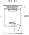
- FIGS. 28, 29, 30 and 31 show another modification of three-layer construction.
- This modification comprises an upper layer which is a coil sheet 1 (FIG. 29) having a conductor 3 corresponding to the first conductor 3-1, an intermediate layer which is a sheet insulator 21 (FIG. 30) having an external conduction line 50, and a lower layer which is a coil sheet 1 (FIG. 31) having first and second conductors 3-1, 3-2 spirally wound in a direction opposite to the winding direction of the conductor of the upper layer when seen from above at the same side of insulators.
- the coil sheets are stacked up.
- the conductor 3 of the upper-layer and the first conductor 3-1 of the lower layer form a two-terminal series circuit, and the second conductor 3-2 of the lower-layer provides a two-terminal circuit.
- the upper-layer coil sheet is of the third type, while the lower-layer coil sheet is of the first type.
- the inner end of the conductor 3 of the upper layer is connected to the inner end of the conductor 3-1 of the lower layer via a plated through hole 4′ of the insulator 21 and a plated through hole 4′ of the lower layer.
- the outer end of the same conductor extends into an external conduction line 40 on the upper layer.
- the inner end of the second conductor 3-2 of the lower layer is connected to an external conduction line 50 on the insulator 21 via a plated through hole in the insulator 21.
- the outer ends of the first and second conductors 3-1, 3-2 of the lower layer extend into external conduction lines 40, 50 on the same layer.
- the external conduction line of the intermediate layer and the conductors of the lower layer are shown in the same manner as above.
- the overall circuit construction of conductors of the layers is shown in FIG. 28 in the same manner as already stated.
- Such coil sheets of the modification of FIGS. 28 to 31 are assembled or stacked up to form specified circuits.
- FIGS. 32, 33, 34 and 35 show still another modification of three-layer construction.
- This modification comprises stacked layers, i.e., an upper-layer which is a coil sheet (FIG. 33) having a conductor 3 corresponding to the first conductor 3-1, an intermediate-layer which is a coil sheet 1 (FIG. 34) having first and second conductors 3-1, 3-2 spirally wound in a direction opposite to the winding direction of the above conductor 3, and a lower layer which is a coil sheet 1 (FIG. 35) having a conductor 3 spirally wound in a specified direction and corresponding to the second conductor 3-2.
- the conductor 3 of the upper layer and the first conductor 3-1 of the intermediate layer provide a two-terminal series circuit.
- the second conductor 3-2 of the intermediate layer and the conductor 3 of the lower-layer provide another two-terminal series circuit.
- the coil sheets of the upper and lower layers are those of the third type, and the coil sheet of the intermediate-layer is of the first type.
- the inner end of the conductor 3 of the upper-layer is connected to the inner end of the first conductor 3-1 of the intermediate-layer via a plated through hole 4′.
- the inner end of the second conductor 3-2 of the intermediate layer is connected to the inner end of the conductor 3 of the lower layer via a plated through hole 5′.
- the outer end of the conductor of each layer extends into an external conduction line 40 or 50 on the corresponding layer.
- the conductors of the intermediate and lower layers are illustrated in the same manner as above.
- the overall circuit construction of the conductors on the layers of the present modification is shown in FIG. 32 in the same manner as above.
- Such coil sheets of the modification of FIGS. 32 to 35 are assembled or stacked up to form specified circuits.
- the conductors of the present invention are in the form of the first and second conductors or conductors corresponding to these conductors. These conductors are usable to provide two winding systems (primary and secondary) and also three or more winding systems (including tertiary, quaternary and additional windings), i.e., multiplicity of winding systems.
- the coil 10 of any of the types shown in FIG. 12 et. seq. and embodying the invention can be mounted on a ferrite or like core 8 as shown in FIGS. 12, 15, 18, 28 and 32 to make a transformer.
- holes are formed in the insulators 2 or 21 for inserting the legs of the core 8 therethrough.
- FIGS. 12, 15, 18, 28 and 32 show a core member 8a in the form of a separate flat plate for use in combination with the core 8.
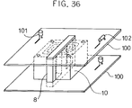
- the coil 10 may be mounted between printed circuit boards 100,100. This embodiment is illustrated in FIG. 36 in which a condenser is designated 101 and a resistor is designated 102.
Landscapes
- Engineering & Computer Science (AREA)
- Power Engineering (AREA)
- Coils Or Transformers For Communication (AREA)
Applications Claiming Priority (4)
| Application Number | Priority Date | Filing Date | Title |
|---|---|---|---|
| JP60010/91 | 1991-03-25 | ||
| JP03060010A JP3074316B2 (ja) | 1991-03-25 | 1991-03-25 | シートコイル積層或いは積装品 |
| JP188634/91 | 1991-07-29 | ||
| JP18863491A JPH05159933A (ja) | 1991-07-29 | 1991-07-29 | コイル |
Publications (2)
| Publication Number | Publication Date |
|---|---|
| EP0506362A2 true EP0506362A2 (fr) | 1992-09-30 |
| EP0506362A3 EP0506362A3 (en) | 1994-05-18 |
Family
ID=26401079
Family Applications (1)
| Application Number | Title | Priority Date | Filing Date |
|---|---|---|---|
| EP19920302568 Withdrawn EP0506362A3 (en) | 1991-03-25 | 1992-03-25 | Coil |
Country Status (2)
| Country | Link |
|---|---|
| US (1) | US5402098A (fr) |
| EP (1) | EP0506362A3 (fr) |
Cited By (7)
| Publication number | Priority date | Publication date | Assignee | Title |
|---|---|---|---|---|
| US5801611A (en) * | 1995-09-14 | 1998-09-01 | U.S. Philips Corporation | Inductive device |
| EP0795184A4 (fr) * | 1994-12-01 | 1998-12-16 | Northrop Grumman Corp | Transformateur d'impulsions de forme plane |
| WO1999031682A3 (fr) * | 1997-12-17 | 1999-08-19 | Koninkl Philips Electronics Nv | Transformateur plan |
| WO2000034734A1 (fr) * | 1998-11-26 | 2000-06-15 | Abb Atom Ab | Composant de mesure electrique et son utilisation |
| GB2369251A (en) * | 2000-05-22 | 2002-05-22 | Payton Ltd | Method of insulating a planar coil circuit |
| EP1211701A1 (fr) * | 2000-12-04 | 2002-06-05 | C.R.F. Società Consortile per Azioni | Inducteur plan à noyau ferromagnétique et son procédé de fabrication |
| US6541964B1 (en) | 1998-11-26 | 2003-04-01 | Westinghouse Atom Ab | Method and apparatus for determining hydride content in a measurement object |
Families Citing this family (20)
| Publication number | Priority date | Publication date | Assignee | Title |
|---|---|---|---|---|
| JP3158757B2 (ja) * | 1993-01-13 | 2001-04-23 | 株式会社村田製作所 | チップ型コモンモードチョークコイル及びその製造方法 |
| US5652561A (en) * | 1993-06-29 | 1997-07-29 | Yokogawa Electric Corporation | Laminating type molded coil |
| EP0689214B1 (fr) * | 1994-06-21 | 1999-09-22 | Sumitomo Special Metals Co., Ltd. | Procédé de fabrication de substrat à enroulements imprimés à multicouches |
| US6000128A (en) * | 1994-06-21 | 1999-12-14 | Sumitomo Special Metals Co., Ltd. | Process of producing a multi-layered printed-coil substrate |
| US5990776A (en) * | 1994-12-08 | 1999-11-23 | Jitaru; Ionel | Low noise full integrated multilayers magnetic for power converters |
| US5631822A (en) * | 1995-08-24 | 1997-05-20 | Interpoint Corporation | Integrated planar magnetics and connector |
| US5777539A (en) * | 1995-09-27 | 1998-07-07 | International Business Machines Corporation | Inductor using multilayered printed circuit board for windings |
| KR970023496A (ko) * | 1995-10-12 | 1997-05-30 | 김봉균 | 네온 트랜스포머의 부하측 고장검출방법 및 그 장치 |
| US5781093A (en) * | 1996-08-05 | 1998-07-14 | International Power Devices, Inc. | Planar transformer |
| US6073339A (en) * | 1996-09-20 | 2000-06-13 | Tdk Corporation Of America | Method of making low profile pin-less planar magnetic devices |
| DE19741302A1 (de) * | 1997-09-19 | 1999-03-25 | Inst Halbleiterphysik Gmbh | Geometrie für planare Induktivitäten |
| US6588090B1 (en) * | 1999-06-03 | 2003-07-08 | Nikon Corporation | Fabrication method of high precision, thermally stable electromagnetic coil vanes |
| US6501363B1 (en) | 1999-11-03 | 2002-12-31 | Innosys, Inc. | Vertical transformer |
| JP2002270437A (ja) * | 2001-03-08 | 2002-09-20 | Tdk Corp | 平面コイルおよび平面トランス |
| US7164349B2 (en) * | 2003-11-07 | 2007-01-16 | Nippon Soken, Inc. | Approaching object detection apparatus |
| CN101171652B (zh) * | 2005-05-03 | 2014-03-05 | 皇家飞利浦电子股份有限公司 | 用于平面型变压器和感应器的绕组装置 |
| US20090189727A1 (en) * | 2008-01-29 | 2009-07-30 | Inventec Corporation | Inductor device |
| US20100237976A1 (en) * | 2009-03-17 | 2010-09-23 | Li Chiu K | Low-profile inductive coil and methond of manufacture |
| JP4893975B2 (ja) * | 2009-08-25 | 2012-03-07 | サンケン電気株式会社 | コイル装置 |
| US11756718B2 (en) * | 2018-12-30 | 2023-09-12 | Texas Instruments Incorporated | Galvanic isolation of integrated closed magnetic path transformer with BT laminate |
Family Cites Families (11)
| Publication number | Priority date | Publication date | Assignee | Title |
|---|---|---|---|---|
| US3133249A (en) * | 1964-05-12 | figure | ||
| US4494100A (en) * | 1982-07-12 | 1985-01-15 | Motorola, Inc. | Planar inductors |
| JPS59189212U (ja) * | 1983-05-18 | 1984-12-15 | 株式会社村田製作所 | チツプ型インダクタ |
| US4593245A (en) * | 1983-12-12 | 1986-06-03 | General Electric Company | Eddy current method for detecting a flaw in semi-conductive material |
| GB2163603A (en) * | 1984-08-25 | 1986-02-26 | Stc Plc | Miniature transformer or choke |
| GB2173956B (en) * | 1985-03-29 | 1989-01-05 | Plessey Co Plc | Improvements relating to electric transformers |
| EP0267108A1 (fr) * | 1986-10-31 | 1988-05-11 | Digital Equipment Corporation | Transformateur miniature |
| US4959631A (en) * | 1987-09-29 | 1990-09-25 | Kabushiki Kaisha Toshiba | Planar inductor |
| US5126707A (en) * | 1989-12-25 | 1992-06-30 | Takeshi Ikeda | Laminated lc element and method for manufacturing the same |
| GB9017910D0 (en) * | 1990-08-15 | 1990-09-26 | Vaseal Electronics Limited | Improvements in and relating to proximity switches |
| US5237165A (en) * | 1991-04-05 | 1993-08-17 | Tingley Iii Loyal H | Multi-turn coil structures and methods of winding same |
-
1992
- 1992-03-23 US US07/855,536 patent/US5402098A/en not_active Expired - Fee Related
- 1992-03-25 EP EP19920302568 patent/EP0506362A3/en not_active Withdrawn
Cited By (10)
| Publication number | Priority date | Publication date | Assignee | Title |
|---|---|---|---|---|
| EP0795184A4 (fr) * | 1994-12-01 | 1998-12-16 | Northrop Grumman Corp | Transformateur d'impulsions de forme plane |
| US5801611A (en) * | 1995-09-14 | 1998-09-01 | U.S. Philips Corporation | Inductive device |
| WO1999031682A3 (fr) * | 1997-12-17 | 1999-08-19 | Koninkl Philips Electronics Nv | Transformateur plan |
| US6307457B1 (en) | 1997-12-17 | 2001-10-23 | U.S. Philips Corporation | Planar transformer |
| WO2000034734A1 (fr) * | 1998-11-26 | 2000-06-15 | Abb Atom Ab | Composant de mesure electrique et son utilisation |
| US6541964B1 (en) | 1998-11-26 | 2003-04-01 | Westinghouse Atom Ab | Method and apparatus for determining hydride content in a measurement object |
| GB2369251A (en) * | 2000-05-22 | 2002-05-22 | Payton Ltd | Method of insulating a planar coil circuit |
| GB2369251B (en) * | 2000-05-22 | 2004-03-24 | Payton Ltd | Planar coil circuit |
| US6882260B2 (en) | 2000-05-22 | 2005-04-19 | Payton Ltd. | Method and apparatus for insulating a planar transformer printed circuit and lead frame windings forms |
| EP1211701A1 (fr) * | 2000-12-04 | 2002-06-05 | C.R.F. Società Consortile per Azioni | Inducteur plan à noyau ferromagnétique et son procédé de fabrication |
Also Published As
| Publication number | Publication date |
|---|---|
| US5402098A (en) | 1995-03-28 |
| EP0506362A3 (en) | 1994-05-18 |
Similar Documents
| Publication | Publication Date | Title |
|---|---|---|
| US5402098A (en) | Coil | |
| US5251108A (en) | Laminated electronic device with staggered holes in the conductors | |
| US8910373B2 (en) | Method of manufacturing an electromagnetic component | |
| US3002260A (en) | shortt etal | |
| US6420953B1 (en) | Multi-layer, multi-functioning printed circuit board | |
| EP0433176A2 (fr) | Circuit hybride multi-couche | |
| EP0759204A1 (fr) | Inducteurs integres a fort facteur de surtension | |
| JPH05101938A (ja) | 積層型コイル及びその製造方法 | |
| US5479146A (en) | Pot core matrix transformer having improved heat rejection | |
| JPH0296312A (ja) | 絶縁されたアモルファス金属リボンを使用した集積電力キャパシタおよびインダクタ/変成器 | |
| JPH056829A (ja) | 薄型トランス | |
| JP4368352B2 (ja) | 電磁遅延線のインダクタンス素子 | |
| US5694104A (en) | Low profile high power surface mount transformer | |
| JPH088180B2 (ja) | 基板実装用小型変成器 | |
| JPH0653055A (ja) | 導電体と導電ランで構成された電磁巻線 | |
| JPH06215962A (ja) | トランス | |
| JPH08293417A (ja) | プリントコイル部品及びプリントコイル基板 | |
| JP2971943B2 (ja) | 薄型トランス | |
| JP3074316B2 (ja) | シートコイル積層或いは積装品 | |
| GB2272109A (en) | Laminated coiled conductive pattern and terminal arrangement | |
| JP3383930B2 (ja) | 薄膜コイルおよび薄膜コイル実装モジュール | |
| JP2810812B2 (ja) | 分岐回路 | |
| JP3109414B2 (ja) | チップアンテナの製造方法 | |
| JPH05315152A (ja) | 積層型コイル | |
| JP2003197430A (ja) | 積層型シートコイル、トランス |
Legal Events
| Date | Code | Title | Description |
|---|---|---|---|
| PUAI | Public reference made under article 153(3) epc to a published international application that has entered the european phase |
Free format text: ORIGINAL CODE: 0009012 |
|
| AK | Designated contracting states |
Kind code of ref document: A2 Designated state(s): DE FR GB |
|
| PUAL | Search report despatched |
Free format text: ORIGINAL CODE: 0009013 |
|
| AK | Designated contracting states |
Kind code of ref document: A3 Designated state(s): DE FR GB |
|
| 17P | Request for examination filed |
Effective date: 19941004 |
|
| 17Q | First examination report despatched |
Effective date: 19970130 |
|
| STAA | Information on the status of an ep patent application or granted ep patent |
Free format text: STATUS: THE APPLICATION IS DEEMED TO BE WITHDRAWN |
|
| 18D | Application deemed to be withdrawn |
Effective date: 20020116 |