EP0507066A1 - Gegenseitige Besitzrechtsverriegelung für Cache-Dateneinheiten - Google Patents
Gegenseitige Besitzrechtsverriegelung für Cache-Dateneinheiten Download PDFInfo
- Publication number
- EP0507066A1 EP0507066A1 EP92102825A EP92102825A EP0507066A1 EP 0507066 A1 EP0507066 A1 EP 0507066A1 EP 92102825 A EP92102825 A EP 92102825A EP 92102825 A EP92102825 A EP 92102825A EP 0507066 A1 EP0507066 A1 EP 0507066A1
- Authority
- EP
- European Patent Office
- Prior art keywords
- data unit
- ownership
- cache
- store
- cpu
- Prior art date
- Legal status (The legal status is an assumption and is not a legal conclusion. Google has not performed a legal analysis and makes no representation as to the accuracy of the status listed.)
- Withdrawn
Links
Images


Classifications
-
- G—PHYSICS
- G06—COMPUTING OR CALCULATING; COUNTING
- G06F—ELECTRIC DIGITAL DATA PROCESSING
- G06F12/00—Accessing, addressing or allocating within memory systems or architectures
- G06F12/02—Addressing or allocation; Relocation
- G06F12/08—Addressing or allocation; Relocation in hierarchically structured memory systems, e.g. virtual memory systems
- G06F12/0802—Addressing of a memory level in which the access to the desired data or data block requires associative addressing means, e.g. caches
- G06F12/0806—Multiuser, multiprocessor or multiprocessing cache systems
- G06F12/0811—Multiuser, multiprocessor or multiprocessing cache systems with multilevel cache hierarchies
Definitions
- the invention relates to an ownership change control particularly according to the preamble of claims 1 and 12.
- Any processor in a data processing system can be an exclusive owner of a data unit in the system storage hierarchy.
- Exclusive ownership of a data unit restricts to one of plural processors in the system the ability to write in the data unit, and only one processor at a time can have exclusive ownership.
- the exclusive ownership of a data unit can be changed from one processor to another processor at the request of a processor, and the ownership can be changed from exclusive to public ownership, and visa-versa.
- Public ownership allows all processors to read, but not to write in, the data unit.
- the invention insures data integrity in a data processing system by providing an ownership interlock on the data units in a store-in type of cache. The ownership interlock prevents any change to occur in the exclusive ownership of a cache data unit until all stores have been made in the cache data unit, and thereafter ownership may be changed.
- the store-in type of cache has been used in computer systems because it requires less bandwidth for its memory bus (between the memory and the cache) than is required by a store-through type of cache for the same frequency of processor accesses.
- Each cache location may be assigned to a processor request and receive a copy of a data unit fetched from system main memory or another cache in the system.
- a processor stores into a data unit in a cache location without storing into the correspondingly addressed data unit in main memory, so that the cache location may become the only location in the system containing the latest version of that data unit.
- the processor may make as many stores (changes) in the data unit as its executing program requires.
- the integrity of data in the system requires that the latest version of the data unit be used for any subsequent processing of the data unit.
- Exclusive ownership (authority) of a data unit has been required in prior store-in caches before allowing writing in the data unit.
- a store-through type of cache is used only for fetching and all store accesses pass through it to the next level (another cache or main storage) in the system storage hierarchy.
- a store-through cache usually has stores performed in it as they pass through it, in order to maintain the latest version of data for obtaining the fastest fetching by its processor.
- Exclusive ownership (authority) to change a cache data unit is assigned to a processor before it is allowed to perform its first store operation in the data unit.
- the assignment of processor ownership has been controlled by setting an exclusive flag bit in a cache directory (sometimes called a tag directory) associated with the respective data unit in the cache.
- the flag bit can be set to indicate either exclusive ownership or public ownership (sometimes called "read-only authority").
- Exclusive ownership by a processor allows only it to write into the data unit.
- the public (read-only) ownership of a data unit does not allow any processor to store into that data unit, but allows each processor in the system to read that data unit which is then sharable by all processors.
- Patent 4,394,731 (PO9-80-016) to Flusche et al teaches the use of exclusive/readonly flags in private processor directories used with private store-in caches and teaches the use of copy directories for processor identification.
- Patent 4,394,731 used copies of all processor private L1 directories for identifying processor ownership and for controlling changes in the ownership of a data unit. Cross-interrogation was used among the copy directories to identify which processor had exclusive ownership of a data unit, and cross-invalidation was used from any identified processor's copy directory to its L1 cache to invalidate its conflicting address to assure exclusivity to a requesting processor, when changing the ownership from exclusive to public readonly ownership, or visa versa.
- a store-in cache updates (writes in) a cache data unit which has its old version located at an associated address in main memory.
- the updated data unit is no longer needed in the cache, it is castout of the cache by writing the updated cache version over the old version of the data unit at the associated address in main memory.
- the cast-out operation is done when an updated data unit is in a cache location which is to be reallocated to another data unit (e.g. fetched from another main memory address).
- a processor may request to store into a data unit not currently in the cache. Then the requested data unit must be fetched from main memory (or from another cache) using the requested address and stored in a newly assigned cache location.
- the cache assignment of a location for the new data unit will be in a cache location not in current use if one can be found. However, only a limited number of cache locations exist, and all may currently contain updated data units. If all the assignable cache locations are currently occupied with changed data units, then one of them must be reassigned for the new request for a data unit not currently in the cache. Then a castout to main memory is required of the updated cache data unit before the reassigned cache location can be made available for use by the new request.
- the castout process is an example of a change of ownership in a data unit, because the castout data unit has its ownership changed from an exclusive processor ownership to a main memory ownership.
- This problem is not generally applicable to a store-through type of cache, since any stores made in it will also have been made in its backing memory, which may be another cache (store-in or store-through) or may be main memory.
- a change in the ownership of any data unit is controlled by the processor request process in a system.
- Only one of the plural processors in a multiprocessing (MP) system can have exclusive ownership (write authority) at any one time over any data unit.
- the exclusive ownership over any data unit may be changed from one processor to another when a different processor requests exclusive ownership.
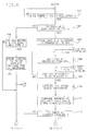
- the prior mechanism for indicating exclusive ownership for a processor was to provide an exclusive (EX) flag bit in each L1 directory entry in a processor's private L1 cache; and the EX bit was set on to indicate which of the associated data units were "owned” by that processor.
- the reset state of the EX flag bit indicated public ownership, which was called "readonly authority" for the associated data unit that made it simultaneously available to all processors in the system.
- each valid data unit in any processor's private L1 cache had either exclusive ownership or public ownership.
- interlock controls there are many types of interlock controls in the prior art.
- One type of prior interlock control requires a castout for a changed cache data unit from a store-in cache to main storage to occur before a new data unit may be represented by the same cache directory entry, which will be overlayed for the new entry. Whether the data unit is changed has been indicated by a change flag bit in an accessed cache directory entry (indicating its associated data unit has been changed).
- the invention deals with a high-speed pipelined computer system in which multiple machine cycles of delay intervenes between the time a store command is generated by a processor and the time its store is made in a target cache data unit.
- a delayed store command is called an "outstanding store” or a "pending store” during its flight time from its generation until it is stored in its targeted data unit in a store-in cache.
- This invention requires that all outstanding changes be made in a data unit by a processor exclusively owning the data unit in a store-in-cache before the ownership of the data unit can be changed to a different processor.
- Outstanding stores are caused by a store command pipeline provided between a processor and the cache to buffer stores in a manner that improves the efficiency of processor operation, such as by freeing the processor to do other processing as soon as it generates each store command.
- the object of the invention is to provide an ownership interlock that prevents changes in the ownership of a data unit in a store-in-cache until all outstanding stores have been made in the cache data unit.
- This invention aids system efficiency by permitting a pipelined store stack to receive store requests from a processor in a continuous manner. Without this invention, the processor would need to stop sending store commands to the store stack when the processor receives an XI signal (for invalidating any XI addressed entry in its L1 cache directory) until all outstanding store commands then in the stack are completed in the cache to assure the integrity of data in the system. Such stoppage of a processor's store operations upon each received XI signal would reduce the rate at which stores are generated in the system and the rate stores could be received by an L2 cache, with a resulting significant loss in system efficiency.
- Processor ownership over a data unit is considered to change: 1. when the requested data unit is found in a cache location which needs to be reassigned and have its ownership changed to the requesting processor in the cache directory; or 2. when the requested data unit is not found in the cache and a cache location containing a changed data unit is reassigned to the requested data unit, so that the changed data unit must be castout before the requested data unit is fetched into the same cache location, thereby changing the ownership of both the castout data unit and the requested data unit.
- the invention may be used with different types of ownership indications for each data unit in a multiple processor system. Ownership may be expressed in a number of different ways, such as by the use of a CPU identifier (CPID) field in each directory entry to identify which of plural CPUs owns the associated data unit exclusively or whether the data unit is owned publicly by all CPUs. Or CPU ownership may be indicated by copies of CPU private L1 directories which are cross-interrogated by all CPU requests in the system to determine which CPU exclusively owns the requested data unit (by its copy directory indicating its exclusive ownership, or indicating the requested data unit is publicly owned).
- the CPID ownership-indicating method centralizes the system coherence control in a single shared directory which is not done in the copy directory method.
- a cache data unit can have its ownership transferred from a currently owning processor to a requesting processor when the rules of ownership change are followed.
- CPID is used in a single system directory, only that CPID field needs to be changed.
- copy directories are used to indicate ownership, a requested data unit has to be moved from one CPU's L1 cache, L1 directory and L1 copy directory (where the data unit is found) to the requesting CPU's L1 cache, L1 directory and copy directory.
- These different data unit ownership methods may be used in a multiple processor system using only private CPU L1 caches and having a shared single system directory, or they may be used in a multiple processor system using private CPU L1 caches and a shared L2 cache having the shared single system directory. Both of these methods require the use of a change field in each directory entry of a cache to indicate if the associated data unit has been changed.
- the preferred embodiment uses the CPID ownership-indicating method in a system using an L2 store-in-cache shared by a plurality of CPUs having private L1 store-through caches.
- the L2 cache uses hardware in the storage control element, SCE, to send a specific cross-invalidate (XI) signal to the current exclusive-owning processor indicated by the current CPID field in the L2 entry for changing the exclusive-ownership of a data unit.
- SCE storage control element
- the XI receiving processor must provide an XI response to determine when all stores must be completed in the accessed L2 data unit before its CPID can be changed in the L2 directory entry.
- a store command may be made to any L2 entry currently indicating exclusive ownership by the CPU, and the store is made concurrently in both the requested L1 cache and the L2 cache, although it takes longer to make the store in the L2 cache than the L1 cache because of a pipelined store stack in the SCE for stacking plural store commands from each processor. Although the store stack delays making the stores in L2, it immediately frees up the processor so it can do another operation.
- a specific XI signal to the CPU requires the CPU to give up ownership of the XI addressed data unit. However, it does not require the CPU to give up ownership instantly. The CPU can finish up any required operations to that data unit before giving up ownership and sending an XI response.
- a CPU presumes it has given up ownership of an L2 cache location at the time it sends an XI response signal. However, one or more of the CPU's outstanding stores to the XI addressed data unit may not yet have been made in the L2 cache, because these stores may still be in the pipeline, in a store queue, or in the stack, which delays the outstanding stores from being made immediately in the cache.
- the outstanding stores in the store stack must be received by the intended cache data unit before its ownership is allowed to change. Data integrity in the system would be adversely affected if the ownership of a data unit were allowed to change before any outstanding stores in the stack were made in the data unit, because then the data unit may not have its latest value when it is fetched by a new owner.
- This problem may occur with any store-in cache operating with pipelined processing between a CPU and a cache that causes a delay to stores being made in the cache after the CPU presumes it has ended its exclusive control over a cache location.
- the problem can occur with a CPU private cache (L1) when its stores are delayed by a pipeline operation, such as by having a pipelined input store queue.
- L1 CPU private cache
- this problem can occur with a store-in cache shared by a plurality of CPUs and is particularly pronounced in a shared L2 store-in cache operating with plural store-through L1 caches.
- a CPU may be storing in a location in the L2 cache assigned to a first main memory address, when the cache location is reassigned to a different main memory location by the L2 replacement LRU controls. If the data unit had been changed in the reassigned cache location, that data unit needs to be castout to main memory (L3) to update its associated main memory location before it can be overlayed by newly requested data from a different main memory address. But that data unit cannot be cast-out until it is has completed storing all outstanding store commands issued to it before its CPU provided the XI response, which stores are still in the pipelined stack.
- main memory L3
- This invention aids system efficiency by permitting the store stack to receive input requests in a continuous manner. Without this invention, a CPU would need to stop sending store commands to its store stack when it provides an XI response until all outstanding stores then in the stack are made in the L2 cache in order to assure the integrity of system data. Such stoppage of the store stacks with each XI signal would reduce the rate at which stores would be received by the L2 cache, with a resulting significant loss in system efficiency.
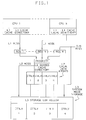
- Fig. 1 represents a multiprocessor system (MP) containing central processing units (CPUs) 1 - N in which each CPU contains at least one private cache and preferably has two private caches, an instruction cache and a data cache. Only the data cache can receive stores, and hence is the cache of concern to the subject invention.
- the instruction cache is readonly.
- the CPU accesses its instructions from its instruction cache and accesses its operand data from its data cache. Both the data cache and instruction cache are used for fetching a data unit requested by their CPU. If a CPU fetch request does not find a requested data unit's address representation in a CPU's L1 cache directory, the L1 cache has a "miss", and the requested address is sent to a shared system cache (L2) to fetch the requested data unit.
- L2 shared system cache
- Each L1 data cache is a store-through type of cache, and hereafter it is referred to as each CPU's L1 cache. If an instruction is to be stored into, it is done only in the instruction's data unit in the L2 cache, and then that data unit is fetched into the requesting instruction cache as a readonly data unit.
- L2 requests comprise all L1 fetch misses and all I/O requests. If an L2 request is not found in the L2 cache, then the L2 cache has a "miss", and the requested address is sent to system main storage (L3), from which the requested data unit is fetched and is sent on the memory bus to the L2 cache, and the L1 data unit is sent to the requesting L1 cache generating the request.
- L3 system main storage
- the data unit for the L1 cache need not be the same size as the data unit in the L2 cache which contains the L1 data unit. Thus each L1 data unit may be sub-multiple of an L2 data unit, or they may be the same size.
- the L2 directory contains an input priority circuit that receives all requests to the L2 cache, i.e. for all CPUs and all I/O devices.
- the priority circuit selects one request at a time for accessing in the L2 cache directory.
- a high-order field in the selected request selects a row (congruence class) in the L2 directory (not shown) and a comparison with an address portion finds any assigned cache directory entry and associated cache data unit location, as is conventionally done in set associative caches so these cache contained items are not shown herein.
- Each L1 and L2 cache herein is presumed to be a 4-way set associative cache.
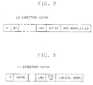
- Each L2 directory entry contains the fields shown in Fig. 2, and each L1 directory entry contains the fields shown in Fig. 3.
- Each L2 entry contains a CPU identifier (CPID) field (e.g. three bits) which are combinatorially set to a value (e.g. 1 to 6) that can identify one CPU in the MP which is the current exclusive owner of the corresponding data unit in the L2 cache.
- CPID CPU identifier
- a zero value in the CPID field indicates a public ownership for the corresponding L2 data unit.
- a conventional LRU replacement circuit (not shown) allocates a replacement entry for each congruence class in which it candidates one of the four entries as the next entry in the congruence class for allocation to a requested data unit that must be fetched from L3 memory.
- the candidate entry is a currently invalid entry, but if there are no invalid entries, it selects the LRU entry of the four entries.
- any old data unit existing in that slot (represented by the current content of the L2 directory entry) must be checked in the directory entry to determine if it has changed data. This is done by checking the state of a change field (i.e. change bit) in the contents of the L2 entry before the entry is changed to represent the newly requested data unit. If the old data unit has been changed (as indicated by its CHG bit), it is the latest version of the old data unit which must be castout to the same address in main memory before the newly requested data unit can be stored in the associated location in the cache.
- a change field i.e. change bit
- Fig. 1 generally illustrates a multiprocessor (MP) computer system which may contain the subject invention. It includes N number of CPUs each having a private store-through cache (L1) with its L1 cache directory. Each CPU accesses storage fetch requests in its L1 cache as long as it obtains cache hits indicating the requested data is available in its L1 cache.
- MP multiprocessor
- the fetch request is sent to the next level in the system storage hierarchy, which is the L2 cache in Fig. 1, to fetch the requested data unit, and is put into a request register, REQ 1 - REQ N, associated with the requesting CPU.
- the CPU request also indicates the type of ownership which is being requested of the data unit to be fetched, which may be either exclusive or readonly.
- the CPU may make store commands for storing data into the data unit.
- a store command usually does not overwrite the entire data unit in either the L1 or L2 cache, but writes only changed byte(s) into the data unit (which may, for example, contain dozens of bytes). This manner of writing into a data unit is well known in the art, using mark bits in the store command to represent the parts of a data unit to be changed by a given store command.
- an I/O request register receives all input and output (I/O) device requests to memory.
- An I/O request accesses the L2 cache since the latest version of a data unit may reside in the L2 cache, where it may be changed by the I/O request. If the I/O request is not in L2, it is then accessed in the L3 main memory without accessing the data unit into the L2 cache.
- REQ 1 - REQ K present their contained requests to the input priority circuit of the L2 shared cache.
- the presented requests are sequenced by the priority circuit, which presents one request at a time, to the L2 cache directory for accessing on a machine cycle or subcycle basis.
- Figs. 4 and 5 show the hardware pipeline for an embodiment of the invention contained in each of the CPUs and the SCE shown in Fig. 1.
- the store pipeline in Figs. 4 and 5 connects the stores from any CPU to the shared L2 cache.
- the nomenclature CPx is used in Figs. 4 and 5 to designate any of the N number of CPUs that is currently receiving an XI signal from the SCE.
- Each CPU store command causes storing in both the respective CPU's L1 cache and in the shared L2 cache.
- the manner of storing in L1 may be conventional.
- Fig. 4 shows a store queue 26 which receives the store commands from its CPx in FIFO order, and sends them to a store stack 27 (located in the SCE, which is the L2 cache and L3 main memory controller) which is in Fig. 5.
- the stack outputs its oldest store command to the L2 priority circuit for accessing in the L2 directory and L2 cache.
- Each store command in the store queue 26 and store stack 27 contains both the address and the data for a single store operation.
- INPTR & OUTPTR inpointer and outpointer registers
- INPTR locates the current entry in the stack for receiving the next store from queue 26.
- OUTPTR locates the oldest store in stack 27 to be outputted to the L2 cache.
- INPTR is incremented each time a store is received in the current inpointer location, and OUTPTR is incremented each time a store is outputted from the stack.
- Both the INPTR and OUTPTR wrap in the stack so that the stack never runs out of space for a next entry. This type of stack pointer control is conventional.
- the CPz, CORn or IOy request command registers 1z, 1n or 1y respectively receive the L1 CPU fetch requests, L2 cache LRU replacement requests and I/O device requests for accesses in the L2 cache.
- Each request command i.e. requestor
- the registers 1z, 1n and 1y represent different types of request registers, of which only one register is doing a request into the L2 cache at any one time in the embodiment.
- One of these registers is selected at a time by the L2 priority circuit for a current access cycle for accessing an entry in the L2 directory and its associated cache slot that contains the associated data unit.
- CPz request register 1z represents any L2 request register that receives any CPU request to L2.
- the subscript z indicates the CPU is a requesting CPU, while the subscript x is used herein to indicate any CPU which is receiving an XI signal.
- the CORn (castout) register 1n represents any of plural castout request registers that receives a current castout request for L2.
- the subscript n indicates the assigned register of the plural castout registers assigned by an LRU replacement circuit for L2 (not shown) to receive the castout address. Replacement of the content of an L2 entry may be done in the conventional manner when a CPU request does not hit (i.e. misses) in the L2 directory.
- the IOy register 1y represents any of plural registers that is selected by the L2 priority as its current request to the L2 directory. Only I/O requests that hit in L2 are used by this embodiment; an I/O request that does not hit (i.e. misses in the L2 directory) is not fetched into L2, but is then accessed in the L3 main memory in the conventional manner.
- An access 2 in the SCE tests the value of the CPID field in the currently accessed L2 directory entry in the detailed embodiment. If circuit 2 detects the tested CPID value is in the range of 1-6, it indicates an EX ownership by the identified CPU. But if the tested CPID is zero, access 2 has detected a public RO ownership for the data unit represented by currently selected L2 entry.
- exclusive ownership If exclusive ownership is detected by access 2, it invokes the generation of a specific cross-invalidate (XI) signal which is sent only to the one CPx identified by the tested CPID.
- XI cross-invalidate
- a detected CPID value of from 1 to 6 in this embodiment indicates the one CPU in the system having exclusive ownership of the data unit associated with the currently selected L2 directory entry.
- a detected value of zero for the CPID indicates that data unit has public ownership and is therefore is readonly.
- public ownership is detected by access 2, it invokes the generation of a general XI signal which is sent to all CPUs except the requesting CPU.
- the specific XI signal initiated by access 2 is sent only to the CPU identified by the CPID in the L2 directory entry.
- the specific XI signal includes the main memory address (or a representation thereof) for the affected data unit in the receiving processor's cache, an XI type indicator (specific or general), and an identifier (ID TAG) for this L2 request command (requestor) so that the SCE can determine which requestor is responsible for a received XI response.
- the specific XI type indicator also indicates whether the addressed data unit is to be invalidated or changed to public ownership.
- the sending of a specific XI signal sets an "XI response wait mode" latch 8 to "XI wait mode".
- the XI wait caused by a specific XI signal, is ended when the SCE receives the XI response from the XI requestor that sent the XI signal getting the XI response.
- the general XI signal initiated by access 2 is sent to all CPUs except the requesting CPU, and is put into all of the respective XI queues.
- the receiving CPUs will invalidate the XI addressed data unit, if it exists in the L1 cache, and does not provide any XI response.
- the SCE can immediately service its next requestor, because the XI ID tag will allow correlation of each XI response with its requestor by the use of the requestor's ID tag.
- a specific XI signal received by any CPx requires that CPU to stop sending stores to that XI addressed data unit, and give up exclusive ownership. However, the CPU can finish up any required operations to that data unit before giving up ownership. When the CPU reaches a point where it can give up ownership (this does not necessarily mean all store commands in store queue 26 to the XI addressed data unit are done), it outgates the XI signal from the XI queue 21.
- the XI queue 21 gates the invalidation addresses with the XI signal to a compare circuit 22 that compares the XI invalidation address in parallel with all addresses currently in the CPx store queue 26 and generates a compare or no compare signal.
- the XI invalidation address is also used to invalidate any entry in the CPx L1 cache equal to the XI invalidation address.
- circuit 22 If circuit 22 provides a compare equal signal, it activates an "update queue” circuit 23 which stops store queue 26 from sending any store commands to the XI addressed data unit (stores to other data units may continue) and updates store queue 26 to mark those store command(s) to the XI addressed data unit.
- the "update queue” circuit 23 also activates an "XI response” circuit 24 to send an XI response signal to the SCE where it resets the "XI response wait mode" latch 8 to terminate the XI wait mode in the SCE.
- circuit 22 If circuit 22 provides a no compare signal on its output G, it indicates there are no store commands in store queue 26 for the XI addressed data unit, and output signal G activates the "XI response" circuit 24 to send an XI response signal to the SCE where it resets the "XI response wait mode” latch 8 to terminate the XI wait mode in the SCE.
- the reset of wait mode circuit 8 causes it to output a wait mode termination signal which gates comparator 28 to compare the current L2 request address with all addresses currently in the the CPx store stack 27 using a single cycle parallel compare operation.
- a compare-equal (cmpr) signal from circuit 28 to an AND gate 29 inputs the content of an INPTR register into a capture INPTR register 10 that captures the current location in stack 27 available for an input of a current CPU store command. Once the INPTR value is captured, CPx can continue to send store commands to the store stack which will change the INPTR value but not the captured INPTR 10.
- the captured INPTR value indicates the last location in the CPx store stack 27 which may contain the last store command from CPx for the requested data unit, and the OUTPTR value indicates the CPx store stack location having the oldest store from CPx.
- the OUTPTR value is being continuously incremented to continuously output its store command entries to update the L2 cache entries. The incrementing of OUTPTR will cause its contained pointer address to wrap around and finally become equal to the captured INPTR value.
- the captured INPTR value is provided to a pointer comparison circuit 38 which compares it with the stack OUTPTR value as the OUTPTR is incremented to output the store commands to the L2 cache.
- a pointer comparison circuit 38 which compares it with the stack OUTPTR value as the OUTPTR is incremented to output the store commands to the L2 cache.
- an output signal D is provided from pointer compare circuit 15 to set the "store done mode" latch 13 to indicate that the store stack outputting is not yet done.
- an output signal E is provided from circuit 15 to reset the "store done mode” latch 13 to indicate that all possible store commands have been outputted from stack 27 into the cache.
- a current CPz request is detected by circuit 4 to determine if it wants exclusive or public ownership. If CPz wants exclusive ownership then general XI signalling is required to all other CPUs that contain that data unit. (However if the CPUs containing the data unit are specifically known, the general XI signalling need only be sent to them without being sent to the CPUs known not to contain the data unit). If CPz wants public ownership then no XI signalling is required.
- All IOy requests are handled by access 2 merely sending a general XI invalidate signal, which prevents any CPU from interfering with any I/O access in the L2 cache.
- the general XI signal from access 2 is used when there there is no need for any XI response from any of the plural CPUs which may contain the data unit, since none can be doing store commands and all that is needed is L1 invalidation.
- change access circuit 7 detects the change field in the current directory entry only for a CORn request, change access circuit 7 is not used for a CPz or IOy request.
- change access circuit 7 finds the change field indicates no change, then there is no need for a castout (since the data unit is the same in main memory L3), and the directory entry update means 20 can immediately update the directory entry by overlaying its content with information from the CPz request that caused the respective CORn request.
- a switch 17 sends the data unit (castout) to the next storage level L3.
- access 16 can immediately obtain the associated data unit from the cache data arrays for the request, i.e. a switch 18 sends the data unit to CPz for a CPU request, and switch 19 sends the data unit to the requesting channel IOy.
- Directory entry update means 20 is immediately used for a CORn request that finds no change in the associated data unit. But if the directory entry update means 20 is being used for a CPz request, then the update of directory entry content by means 20 is delayed until after the castout has been completed (for system recovery reasons the initial content of the entry may be needed if a system failure should occur before the castout is completed).
- the timing delay for the cache data access 16 is controlled by the output F from the "store done" latch 13 when it is reset by a compare-equal signal E from PTR a compare circuit 15 (when the INPTR and OUTPTR are equal). All CPz store command entries to the requested data unit in stack 27 will have been flushed out to the cache when circuit 15 signals its output signal E, since then the OUTPTR will have revolved back to the captured INPTR starting point for the stack output operation, and then cache data access 16 may be initiated.
- Figs. 6, 7 and 8 are functionally related to the reference numbers used in Figs. 4 and 5, wherein 100 has been added to the latter reference numbers to generate the former reference numbers.
- the following steps in the novel process disclosed herein also are related to the reference numbers in Figs. 4 and 5.
Landscapes
- Engineering & Computer Science (AREA)
- Theoretical Computer Science (AREA)
- Physics & Mathematics (AREA)
- General Engineering & Computer Science (AREA)
- General Physics & Mathematics (AREA)
- Memory System Of A Hierarchy Structure (AREA)
- Advance Control (AREA)
Applications Claiming Priority (2)
| Application Number | Priority Date | Filing Date | Title |
|---|---|---|---|
| US07/680,176 US5490261A (en) | 1991-04-03 | 1991-04-03 | Interlock for controlling processor ownership of pipelined data for a store in cache |
| US680176 | 1991-04-03 |
Publications (1)
| Publication Number | Publication Date |
|---|---|
| EP0507066A1 true EP0507066A1 (de) | 1992-10-07 |
Family
ID=24730015
Family Applications (1)
| Application Number | Title | Priority Date | Filing Date |
|---|---|---|---|
| EP92102825A Withdrawn EP0507066A1 (de) | 1991-04-03 | 1992-02-20 | Gegenseitige Besitzrechtsverriegelung für Cache-Dateneinheiten |
Country Status (3)
| Country | Link |
|---|---|
| US (1) | US5490261A (de) |
| EP (1) | EP0507066A1 (de) |
| JP (1) | JP2566701B2 (de) |
Cited By (3)
| Publication number | Priority date | Publication date | Assignee | Title |
|---|---|---|---|---|
| CN1054223C (zh) * | 1993-12-15 | 2000-07-05 | 硅图像有限公司 | 用于分级数据超高速缓冲存储器系统中同步化的系统和方法 |
| US6988167B2 (en) * | 2001-02-08 | 2006-01-17 | Analog Devices, Inc. | Cache system with DMA capabilities and method for operating same |
| GB2420199A (en) * | 2004-11-15 | 2006-05-17 | Infineon Technologies Ag | Shared cache for a memory on a computing device |
Families Citing this family (55)
| Publication number | Priority date | Publication date | Assignee | Title |
|---|---|---|---|---|
| US6021471A (en) * | 1994-11-15 | 2000-02-01 | Advanced Micro Devices, Inc. | Multiple level cache control system with address and data pipelines |
| EP0681240B1 (de) * | 1994-05-03 | 2001-01-10 | Hewlett-Packard Company | Anordnung mit Duplikat des Cache-Etikettenspeichers |
| JP3132749B2 (ja) * | 1994-12-05 | 2001-02-05 | インターナショナル・ビジネス・マシーンズ・コーポレ−ション | マルチプロセッサ・データ処理システム |
| US5655103A (en) * | 1995-02-13 | 1997-08-05 | International Business Machines Corporation | System and method for handling stale data in a multiprocessor system |
| US5655100A (en) * | 1995-03-31 | 1997-08-05 | Sun Microsystems, Inc. | Transaction activation processor for controlling memory transaction execution in a packet switched cache coherent multiprocessor system |
| US5740399A (en) * | 1995-08-23 | 1998-04-14 | International Business Machines Corporation | Modified L1/L2 cache inclusion for aggressive prefetch |
| US5758119A (en) * | 1995-08-23 | 1998-05-26 | International Business Machines Corp. | System and method for indicating that a processor has prefetched data into a primary cache and not into a secondary cache |
| US6745292B1 (en) * | 1995-12-08 | 2004-06-01 | Ncr Corporation | Apparatus and method for selectively allocating cache lines in a partitioned cache shared by multiprocessors |
| US5680571A (en) * | 1995-12-28 | 1997-10-21 | Unisys Corporation | Multi-processor data processing system with multiple, separate instruction and operand second level caches |
| US6088769A (en) * | 1996-10-01 | 2000-07-11 | International Business Machines Corporation | Multiprocessor cache coherence directed by combined local and global tables |
| US5893161A (en) * | 1996-11-12 | 1999-04-06 | Hewlett-Packard Co. | Method for allocating ownership of portions of memory in a coherent memory system |
| US5890207A (en) * | 1996-11-27 | 1999-03-30 | Emc Corporation | High performance integrated cached storage device |
| US5890219A (en) * | 1996-11-27 | 1999-03-30 | Emc Corporation | Redundant writing of data to cached storage system |
| US5884055A (en) * | 1996-11-27 | 1999-03-16 | Emc Corporation | Method and apparatus including a shared resource and multiple processors running a common control program accessing the shared resource |
| US5778394A (en) * | 1996-12-23 | 1998-07-07 | Emc Corporation | Space reclamation system and method for use in connection with tape logging system |
| US5960455A (en) * | 1996-12-30 | 1999-09-28 | Unisys Corporation | Scalable cross bar type storage controller |
| US5875201A (en) * | 1996-12-30 | 1999-02-23 | Unisys Corporation | Second level cache having instruction cache parity error control |
| US6122711A (en) | 1997-01-07 | 2000-09-19 | Unisys Corporation | Method of and apparatus for store-in second level cache flush |
| US5860093A (en) * | 1997-01-21 | 1999-01-12 | Unisys Corporation | Reduced instruction processor/storage controller interface |
| US5900009A (en) * | 1997-03-21 | 1999-05-04 | Emc Corporation | System and method for accessing records in a cache slot which are associated with a current owner storage element or at least one previous owner storage element |
| US6108752A (en) * | 1997-10-24 | 2000-08-22 | Compaq Computer Corporation | Method and apparatus for delaying victim writes in a switch-based multi-processor system to maintain data coherency |
| US6154816A (en) * | 1997-10-24 | 2000-11-28 | Compaq Computer Corp. | Low occupancy protocol for managing concurrent transactions with dependencies |
| US6122714A (en) * | 1997-10-24 | 2000-09-19 | Compaq Computer Corp. | Order supporting mechanisms for use in a switch-based multi-processor system |
| US6209073B1 (en) | 1998-04-27 | 2001-03-27 | International Business Machines Corp. | System and method for interlocking barrier operations in load and store queues |
| US6341340B1 (en) * | 1998-12-28 | 2002-01-22 | Oracle Corporation | Transitioning ownership of data items between ownership groups |
| US6321238B1 (en) * | 1998-12-28 | 2001-11-20 | Oracle Corporation | Hybrid shared nothing/shared disk database system |
| US6418413B2 (en) * | 1999-02-04 | 2002-07-09 | Ita Software, Inc. | Method and apparatus for providing availability of airline seats |
| TW410295B (en) * | 1999-03-02 | 2000-11-01 | Via Tech Inc | Memory access control device |
| US6493800B1 (en) * | 1999-03-31 | 2002-12-10 | International Business Machines Corporation | Method and system for dynamically partitioning a shared cache |
| US6678838B1 (en) * | 1999-08-23 | 2004-01-13 | Advanced Micro Devices, Inc. | Method to track master contribution information in a write buffer |
| WO2001033472A2 (en) * | 1999-11-01 | 2001-05-10 | Ita Software, Inc. | Method and apparatus for providing availability of airline seats |
| US7562027B1 (en) * | 1999-11-01 | 2009-07-14 | Ita Software, Inc. | Availability processing in a travel planning system |
| US7216085B1 (en) | 2000-07-13 | 2007-05-08 | Ita Software, Inc. | Competitive availability tools |
| US7024520B2 (en) * | 2002-10-03 | 2006-04-04 | Hewlett-Packard Development Company, L.P. | System and method enabling efficient cache line reuse in a computer system |
| US7000080B2 (en) * | 2002-10-03 | 2006-02-14 | Hewlett-Packard Development Company, L.P. | Channel-based late race resolution mechanism for a computer system |
| US7003635B2 (en) * | 2002-10-03 | 2006-02-21 | Hewlett-Packard Development Company, L.P. | Generalized active inheritance consistency mechanism having linked writes |
| US6898676B2 (en) * | 2002-10-03 | 2005-05-24 | Hewlett-Packard Development Company, L.P. | Computer system supporting both dirty-shared and non-dirty-shared data processing entities |
| US6990559B2 (en) * | 2002-10-03 | 2006-01-24 | Hewlett-Packard Development Company, L.P. | Mechanism for resolving ambiguous invalidates in a computer system |
| US6895476B2 (en) * | 2002-10-03 | 2005-05-17 | Hewlett-Packard Development Company, L.P. | Retry-based late race resolution mechanism for a computer system |
| US6892290B2 (en) * | 2002-10-03 | 2005-05-10 | Hewlett-Packard Development Company, L.P. | Linked-list early race resolution mechanism |
| US7051163B2 (en) * | 2002-10-03 | 2006-05-23 | Hewlett-Packard Development Company, L.P. | Directory structure permitting efficient write-backs in a shared memory computer system |
| US7032077B2 (en) * | 2002-12-23 | 2006-04-18 | Hewlett-Packard Development Company, L.P. | Multiple cache coherency |
| US7814065B2 (en) * | 2005-08-16 | 2010-10-12 | Oracle International Corporation | Affinity-based recovery/failover in a cluster environment |
| US7966453B2 (en) * | 2007-12-12 | 2011-06-21 | International Business Machines Corporation | Method and apparatus for active software disown of cache line's exlusive rights |
| WO2011048582A1 (en) * | 2009-10-25 | 2011-04-28 | Plurality Ltd. | Shared cache for a tightly-coupled multiprocessor |
| US10678744B2 (en) * | 2010-05-03 | 2020-06-09 | Wind River Systems, Inc. | Method and system for lockless interprocessor communication |
| US8516200B2 (en) | 2010-09-07 | 2013-08-20 | International Business Machines Corporation | Avoiding cross-interrogates in a streaming data optimized L1 cache |
| US8904118B2 (en) | 2011-01-07 | 2014-12-02 | International Business Machines Corporation | Mechanisms for efficient intra-die/intra-chip collective messaging |
| US20120179896A1 (en) | 2011-01-10 | 2012-07-12 | International Business Machines Corporation | Method and apparatus for a hierarchical synchronization barrier in a multi-node system |
| US20120185672A1 (en) * | 2011-01-18 | 2012-07-19 | International Business Machines Corporation | Local-only synchronizing operations |
| US9195550B2 (en) | 2011-02-03 | 2015-11-24 | International Business Machines Corporation | Method for guaranteeing program correctness using fine-grained hardware speculative execution |
| US9031887B2 (en) | 2012-12-18 | 2015-05-12 | International Business Machines Corporation | Determining a replacement document owner |
| US10705957B1 (en) | 2018-12-19 | 2020-07-07 | International Business Machines Corporation | Selectively updating a coherence state in response to a storage update |
| US10691599B1 (en) | 2018-12-19 | 2020-06-23 | International Business Machines Corporation | Selectively updating a coherence state in response to a storage update |
| US10733102B2 (en) | 2018-12-19 | 2020-08-04 | International Business Machines Corporation | Selectively updating a coherence state in response to a storage update |
Citations (2)
| Publication number | Priority date | Publication date | Assignee | Title |
|---|---|---|---|---|
| EP0329942A2 (de) * | 1988-02-22 | 1989-08-30 | International Business Machines Corporation | Speicherwarteschlange für eine festgekoppelte Mehrprozessorenkonfiguration mit einem zweistufigen Cache-Pufferspeicher |
| EP0416211A2 (de) * | 1989-09-08 | 1991-03-13 | International Business Machines Corporation | Zugangsberechtigungstabelle für Mehrprozessor-Cachespeicher |
Family Cites Families (5)
| Publication number | Priority date | Publication date | Assignee | Title |
|---|---|---|---|---|
| US4622631B1 (en) * | 1983-12-30 | 1996-04-09 | Recognition Int Inc | Data processing system having a data coherence solution |
| EP0348628A3 (de) * | 1988-06-28 | 1991-01-02 | International Business Machines Corporation | Cache-Speicheranordnung |
| DE69127936T2 (de) * | 1990-06-29 | 1998-05-07 | Digital Equipment Corp | Busprotokoll für Prozessor mit write-back cache |
| US5276852A (en) * | 1990-10-01 | 1994-01-04 | Digital Equipment Corporation | Method and apparatus for controlling a processor bus used by multiple processor components during writeback cache transactions |
| US5265232A (en) * | 1991-04-03 | 1993-11-23 | International Business Machines Corporation | Coherence control by data invalidation in selected processor caches without broadcasting to processor caches not having the data |
-
1991
- 1991-04-03 US US07/680,176 patent/US5490261A/en not_active Expired - Fee Related
-
1992
- 1992-02-20 EP EP92102825A patent/EP0507066A1/de not_active Withdrawn
- 1992-02-26 JP JP4039482A patent/JP2566701B2/ja not_active Expired - Lifetime
Patent Citations (2)
| Publication number | Priority date | Publication date | Assignee | Title |
|---|---|---|---|---|
| EP0329942A2 (de) * | 1988-02-22 | 1989-08-30 | International Business Machines Corporation | Speicherwarteschlange für eine festgekoppelte Mehrprozessorenkonfiguration mit einem zweistufigen Cache-Pufferspeicher |
| EP0416211A2 (de) * | 1989-09-08 | 1991-03-13 | International Business Machines Corporation | Zugangsberechtigungstabelle für Mehrprozessor-Cachespeicher |
Non-Patent Citations (1)
| Title |
|---|
| IBM TECHNICAL DISCLOSURE BULLETIN. vol. 33, no. 11, April 1991, NEW YORK US pages 391 - 393; 'Store buffering at second level cache/memory hierarchy' * |
Cited By (4)
| Publication number | Priority date | Publication date | Assignee | Title |
|---|---|---|---|---|
| CN1054223C (zh) * | 1993-12-15 | 2000-07-05 | 硅图像有限公司 | 用于分级数据超高速缓冲存储器系统中同步化的系统和方法 |
| US6988167B2 (en) * | 2001-02-08 | 2006-01-17 | Analog Devices, Inc. | Cache system with DMA capabilities and method for operating same |
| GB2420199A (en) * | 2004-11-15 | 2006-05-17 | Infineon Technologies Ag | Shared cache for a memory on a computing device |
| GB2420199B (en) * | 2004-11-15 | 2007-02-28 | Infineon Technologies Ag | Shared cache for a memory on a computing device |
Also Published As
| Publication number | Publication date |
|---|---|
| JPH0581129A (ja) | 1993-04-02 |
| JP2566701B2 (ja) | 1996-12-25 |
| US5490261A (en) | 1996-02-06 |
Similar Documents
| Publication | Publication Date | Title |
|---|---|---|
| US5490261A (en) | Interlock for controlling processor ownership of pipelined data for a store in cache | |
| EP0507063A1 (de) | Verfahren und Vorrichtung für ein Verzeichnis zum kreuzweisen Ungültigerklären | |
| US4463420A (en) | Multiprocessor cache replacement under task control | |
| US4394731A (en) | Cache storage line shareability control for a multiprocessor system | |
| US5875472A (en) | Address conflict detection system employing address indirection for use in a high-speed multi-processor system | |
| JP2825550B2 (ja) | 多重仮想空間アドレス制御方法および計算機システム | |
| US6249846B1 (en) | Distributed data dependency stall mechanism | |
| EP0372201B1 (de) | Verfahren zum Abrufen von potentiell ungültigen Daten in einem Mehrrechnersystem | |
| EP0828217A1 (de) | Cachespeicherräumungsvorrichtung und hiermit versehenes Rechnersystem | |
| US10083126B2 (en) | Apparatus and method for avoiding conflicting entries in a storage structure | |
| EP0061570A2 (de) | Schreib-in-Pufferspeicher Mehrprozessoranordnung mit Prüfpunkt-Eigenschaft | |
| US8255591B2 (en) | Method and system for managing cache injection in a multiprocessor system | |
| US4631660A (en) | Addressing system for an associative cache memory | |
| CN106897230B (zh) | 用于处理原子更新操作的装置和方法 | |
| JPH11506852A (ja) | 多数のバスマスタと共用レベル2キャッシュとを備える多レベルキャッシュシステムでのキャッシュスヌーピングオーバーヘッドの低減 | |
| US6976148B2 (en) | Acceleration of input/output (I/O) communication through improved address translation | |
| US6105108A (en) | Method and apparatus for releasing victim data buffers of computer systems by comparing a probe counter with a service counter | |
| US6061765A (en) | Independent victim data buffer and probe buffer release control utilzing control flag | |
| JP2001222468A (ja) | マイクロプロセッサのロード/ストア命令制御回路、およびロード/ストア命令制御方法 | |
| US5479629A (en) | Method and apparatus for translation request buffer and requestor table for minimizing the number of accesses to the same address | |
| EP0051745B1 (de) | Pufferspeicherhierarchie für ein Multiprozessorsystem | |
| CN110291507B (zh) | 用于提供对存储器系统的加速访问的方法和装置 | |
| US7363435B1 (en) | System and method for coherence prediction | |
| EP0468804A2 (de) | Steuerungsanordnung eines hierarchischen Speichers | |
| EP0159712A2 (de) | Steuerungsgerät in einem digitalen Computer |
Legal Events
| Date | Code | Title | Description |
|---|---|---|---|
| PUAI | Public reference made under article 153(3) epc to a published international application that has entered the european phase |
Free format text: ORIGINAL CODE: 0009012 |
|
| AK | Designated contracting states |
Kind code of ref document: A1 Designated state(s): DE FR GB |
|
| 17P | Request for examination filed |
Effective date: 19930218 |
|
| STAA | Information on the status of an ep patent application or granted ep patent |
Free format text: STATUS: THE APPLICATION HAS BEEN WITHDRAWN |
|
| 18W | Application withdrawn |
Withdrawal date: 19960715 |