EP0508128A2 - Commutateur intégré monolithique à quatre accès avec des diodes PIN en GaAs - Google Patents
Commutateur intégré monolithique à quatre accès avec des diodes PIN en GaAs Download PDFInfo
- Publication number
- EP0508128A2 EP0508128A2 EP92104080A EP92104080A EP0508128A2 EP 0508128 A2 EP0508128 A2 EP 0508128A2 EP 92104080 A EP92104080 A EP 92104080A EP 92104080 A EP92104080 A EP 92104080A EP 0508128 A2 EP0508128 A2 EP 0508128A2
- Authority
- EP
- European Patent Office
- Prior art keywords
- pin diodes
- pair
- input
- output ports
- bias
- Prior art date
- Legal status (The legal status is an assumption and is not a legal conclusion. Google has not performed a legal analysis and makes no representation as to the accuracy of the status listed.)
- Granted
Links
- 229910001218 Gallium arsenide Inorganic materials 0.000 title claims abstract description 52
- 239000004065 semiconductor Substances 0.000 claims description 16
- 238000000034 method Methods 0.000 abstract description 10
- 239000000758 substrate Substances 0.000 description 6
- 238000002955 isolation Methods 0.000 description 4
- 230000003071 parasitic effect Effects 0.000 description 4
- 238000003780 insertion Methods 0.000 description 3
- 230000037431 insertion Effects 0.000 description 3
- 229910052751 metal Inorganic materials 0.000 description 3
- 239000002184 metal Substances 0.000 description 3
- 229910052710 silicon Inorganic materials 0.000 description 3
- XUIMIQQOPSSXEZ-UHFFFAOYSA-N Silicon Chemical compound [Si] XUIMIQQOPSSXEZ-UHFFFAOYSA-N 0.000 description 2
- 230000015572 biosynthetic process Effects 0.000 description 2
- 239000003990 capacitor Substances 0.000 description 2
- 239000002019 doping agent Substances 0.000 description 2
- 238000004519 manufacturing process Methods 0.000 description 2
- 150000002739 metals Chemical class 0.000 description 2
- 238000012986 modification Methods 0.000 description 2
- 230000004048 modification Effects 0.000 description 2
- 238000001451 molecular beam epitaxy Methods 0.000 description 2
- 239000010703 silicon Substances 0.000 description 2
- -1 InP Chemical class 0.000 description 1
- 230000005540 biological transmission Effects 0.000 description 1
- 230000015556 catabolic process Effects 0.000 description 1
- 238000005229 chemical vapour deposition Methods 0.000 description 1
- 238000005352 clarification Methods 0.000 description 1
- 150000001875 compounds Chemical class 0.000 description 1
- 239000010432 diamond Substances 0.000 description 1
- 238000005530 etching Methods 0.000 description 1
- 230000005669 field effect Effects 0.000 description 1
- 239000010408 film Substances 0.000 description 1
- 238000002513 implantation Methods 0.000 description 1
- 230000010354 integration Effects 0.000 description 1
- 239000000463 material Substances 0.000 description 1
- 239000010409 thin film Substances 0.000 description 1
- 229910052725 zinc Inorganic materials 0.000 description 1
Images

Classifications
-
- H—ELECTRICITY
- H03—ELECTRONIC CIRCUITRY
- H03K—PULSE TECHNIQUE
- H03K17/00—Electronic switching or gating, i.e. not by contact-making and –breaking
- H03K17/51—Electronic switching or gating, i.e. not by contact-making and –breaking characterised by the components used
- H03K17/74—Electronic switching or gating, i.e. not by contact-making and –breaking characterised by the components used by the use, as active elements, of diodes
- H03K17/76—Switching arrangements with several input- or output-terminals, e.g. multiplexers, distributors
-
- H—ELECTRICITY
- H01—ELECTRIC ELEMENTS
- H01P—WAVEGUIDES; RESONATORS, LINES, OR OTHER DEVICES OF THE WAVEGUIDE TYPE
- H01P1/00—Auxiliary devices
- H01P1/10—Auxiliary devices for switching or interrupting
- H01P1/15—Auxiliary devices for switching or interrupting by semiconductor devices
Definitions
- This invention relates to semiconductor electronic integrated circuits, and more particularly, to monolithic microwave switches.
- the PIN diode is a microwave semiconductor diode which can be used as an electrically variable resistor. It can be incorporated in waveguide, coaxial, and stripline components for microwave switching, attenuation, limiting, modulation, and phase shifting. PIN diode switches have been constructed by mounting diodes in series, shunt, or a combination of the two. Historically, hybrid Si PIN diodes have been used in microwave circuits. However, to meet requirement specifications (such as insertion loss), the Si PIN diodes used are extremely small, making them difficult to bond into circuits. The parasitic bond wire inductances used to connect the diodes into the circuit reduce the bandwidth over which the device maintains an acceptable small-signal match. A monolithic device can decrease both the size of the circuit and the parasitic bond wire inductance, however, this has been difficult to achieve in Si.
- the circuit comprises: first and second input ports; first and second output ports; a first pair of back-to-back monolithic GaAs PIN diodes connected between the first input and the first output ports, the first pair of back-to-back monolithic GaAs PIN diodes having a first bias node between the first pair of back-to-back monolithic GaAs PIN diodes; a second pair of back-to-back monolithic GaAs PIN diodes connected between the first input and the second output ports, the second pair of back-to-back monolithic GaAs PIN diodes having a second bias node between the second pair of back-to-back monolithic GaAs PIN diodes; a third pair of back-to-back monolithic GaAs PIN diodes connected between the second input and the first output ports, the third pair of back-to-back monolithic GaAs PIN diodes having a third bias node between
- the back-to-back PIN diode pairs are directly connected between the input ports and the output ports;
- the circuit is no greater than one square millimeter in area;
- the circuit has only two input ports, two output ports, and eight PIN diodes;
- the PIN diodes are fabricated from GaAs;
- external bias circuitry is connected through RF decoupling circuits to the input ports, the output ports and the bias nodes;
- ⁇ /4 chokes are a portion of the bias circuitry;
- the PIN diodes are in a square configuration; and the first input port is a transmit port and the second input port is a receive port and the first and second output ports are antenna ports.
- Monolithic GaAs PIN diodes have demonstrated superior performance in a number of switching and control circuits.
- FET field effect transistor
- FIG. 1 shows a preferred embodiment PIN diode switch schematic. Table 1 below may be referred to for clarification of the element numbers in the drawing.
- the switch has four RF Ports 26,28,30,32 and eight DC Ports 36,38.
- the RF Ports 26,28,30,32 are generically labeled RF Port A-D, however more application specific names could be used.
- RF Port A 26 could be labeled Antenna 1
- RE Port B 28 could be labeled Antenna 2
- RF Port C 30 could be labeled Transmit
- RF Port D 32 could be labeled Receive.
- the switch contains eight PIN diodes 10 in preferably a square or diamond configuration with the diodes connected either anode-to-anode or cathode-to-cathode, oriented as shown in FIG. 1. This method of connection creates a higher breakdown voltage and improved RF power handling.
- the RF Ports 26,28,30,32 are connected externally by bond wires 34, which will exhibit a parasitic inductance.
- the DC Ports 36,38 are connected to approximately 250 ohm on-chip resistors 12 to limit diode current.
- each resistor 12 is connected in series to a bond wire 14, which is connected in series to an approximately 80 ohm ⁇ /4 choke 16 (1/4 wavelength line), which is connected in series to a low reactance capacitor 18, which is tied to ground 20.
- the Bias A 22 and Bias B 24 lines are between the ⁇ /4 chokes 16 and the capacitors 18 in each of the 8 DC Port lines.
- the DC Port lines 36, by the RF Ports 26,28,30,32 are connected to Bias A 22 and the DC Port lines 38, between the two diodes 10 in each switch arm (the two diodes between the RF Ports denote a switch arm for a total of four switch arms) are connected to Bias B 24.
- RF Port D 32 can be switched to either RF Port A 26 or RF Port B 28, while RF Port C simultaneously would be switched to either RF Port B 28 or RF Port A 26, respectively.
- RF Ports C 30 and D 32 cannot both be switched to RF Port A 26 or B 28 at the same time. If 0 volts is applied to both Bias 1 22 and Bias 2 24 all switch arms are "off" (high isolation).
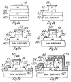
- FIGS. 2a- 2f show a method for fabrication of a vertical GaAs PIN diode, which is a preferred method for this device.
- the PIN diodes are formed on an semi-insulating GaAs substrate 40.
- the layers are preferably epitaxially grown by a metal organic chemical vapor deposition (MOCVD) process.
- MOCVD metal organic chemical vapor deposition
- An alternative process would be molecular beam epitaxy (MBE).
- a n-type layer 42 preferably n+, approximately 0.25 um thick and doped greater than 1018 cm ⁇ 3, is grown over the substrate 40.
- the n+ layer 46 may be doped with dopants such as Si, S, or Se.
- An I (intrinsic) layer 44 is grown over the n+ layer 42.
- a p-type layer 46 preferably p+, approximately 0.25 um thick and doped greater than 1018 cm ⁇ 3, is grown over the I layer 44.
- the p+ layer 46 may be doped with dopants such as Be, Zn, C, Mg, or Mn.
- a p+ contact layer 48 of Au/Zn/Au is deposited on the p-type layer 46 and patterned for the p+ layer 46 contact.
- the p+ contact layer 48 is preferably alloyed for 1 minute at 370°C. Referring to FIG.
- a mesa for the PIN diode is etched to the I layer 44/n+ layer 42 interface using the p+ contact layer 48 as a mask.
- a n+ contact layer 50 of Au/Ge/Ni is deposited on the n+ layer 42 and on the p+ contact layer 48, and patterned to form contact to the n+ layer 42.
- the n+ contact layer 50 is preferably alloyed for 3 minutes at 430°C.
- the diodes are isolated by etching through the n+ layer, as shown in FIG. 2d. Referring to FIGS. 2e and 2f, after the contact metals 48,50 are alloyed, interconnect metals 52, preferably Ti/Au, are patterned and lifted off.
- Ti/Au is then deposited, patterned, and plated to form airbridges and transmission lines 54.
- the number of PIN diodes desired for the circuit may be fabricated in the described manner on a single substrate. This is only one embodiment of PIN diode formation. Any method which results in monolithic PIN diode formation, such as implantation of the p+ and n+ regions, may be used to realize the circuit described above. Also, if desired, the cathode-to-cathode connected diodes could share a common p+ region and the anode-to-anode connected diodes could share a common n+ region.
- the resultant integrated circuit may be placed on a thin-film or thick-film substrate along with the external bias circuitry (with RF decoupling circuits) for integration into a system.
- the GaAs monolithic PIN diode switch described above offers many advantages. Several GaAs PIN diodes can be integrated on a semi-insulating GaAs substrate, while maintaining high isolation between the diodes and achieving low diode parasitic capacitances. This is very difficult to do in silicon. The diodes are heat sunk by the GaAs substrate. This PIN diode switch offers low insertion loss and high isolation, even better than switches made using GaAs FETs or HBTs. The monolithic implementation of this switch offers broader band performance and much smaller size (less than 1 square millimeter in area) than a hybrid switch. External bias circuitry may be used to tune the switch for operation from less than 100 MHz to frequencies above 2 GHz.
Landscapes
- Electronic Switches (AREA)
- Semiconductor Integrated Circuits (AREA)
- Waveguide Switches, Polarizers, And Phase Shifters (AREA)
Applications Claiming Priority (2)
| Application Number | Priority Date | Filing Date | Title |
|---|---|---|---|
| US07/676,649 US5159296A (en) | 1991-03-28 | 1991-03-28 | Four port monolithic gaas pin diode switch |
| US676649 | 1991-03-28 |
Publications (3)
| Publication Number | Publication Date |
|---|---|
| EP0508128A2 true EP0508128A2 (fr) | 1992-10-14 |
| EP0508128A3 EP0508128A3 (en) | 1993-02-03 |
| EP0508128B1 EP0508128B1 (fr) | 1996-06-12 |
Family
ID=24715378
Family Applications (1)
| Application Number | Title | Priority Date | Filing Date |
|---|---|---|---|
| EP92104080A Expired - Lifetime EP0508128B1 (fr) | 1991-03-28 | 1992-03-10 | Commutateur intégré monolithique à quatre accès avec des diodes PIN en GaAs |
Country Status (4)
| Country | Link |
|---|---|
| US (1) | US5159296A (fr) |
| EP (1) | EP0508128B1 (fr) |
| JP (1) | JP3250837B2 (fr) |
| DE (1) | DE69211409T2 (fr) |
Cited By (7)
| Publication number | Priority date | Publication date | Assignee | Title |
|---|---|---|---|---|
| EP0715410A2 (fr) * | 1994-11-28 | 1996-06-05 | Murata Manufacturing Co., Ltd. | Commutateur haute fréquence |
| EP0716509A2 (fr) * | 1994-12-05 | 1996-06-12 | Murata Manufacturing Co., Ltd. | Commutateur haute fréquence |
| EP0763854A1 (fr) * | 1995-08-19 | 1997-03-19 | Daimler-Benz Aktiengesellschaft | Circuit comprenant un arrangement intégré monolithique de diodes PIN/Schottky |
| EP0724333A3 (fr) * | 1995-01-30 | 1998-02-11 | Murata Manufacturing Co., Ltd. | Commutateur haute fréquence hybride pouvant être utilisé dans un téléphone portable du type à diversité d'antennes |
| EP1231670A3 (fr) * | 2001-02-09 | 2002-09-04 | Nokia Corporation | Accord d'une antenne |
| WO2004086623A1 (fr) * | 2003-03-28 | 2004-10-07 | Koninklijke Philips Electronics N.V. | Commutateur h.f. a commande electronique |
| US10219725B2 (en) | 2012-09-04 | 2019-03-05 | Hill-Rom Services, Inc. | Patient mobility surface assessment system and method |
Families Citing this family (13)
| Publication number | Priority date | Publication date | Assignee | Title |
|---|---|---|---|---|
| US5296762A (en) * | 1992-11-04 | 1994-03-22 | Rockwell International Corporation | Bidirectional microwave amplifier apparatus |
| IL105952A (en) * | 1993-06-08 | 1997-02-18 | Univ Ramot | Controlled semiconductor capacitors |
| US5510757A (en) * | 1994-09-23 | 1996-04-23 | Loral Corporation | Broadband miniature transfer switch matrix |
| US5696470A (en) * | 1995-06-07 | 1997-12-09 | Comsat Corporation | Solid-state electronic switching module |
| DE69612041T2 (de) * | 1995-07-24 | 2001-08-02 | Murata Mfg. Co., Ltd. | Hochfrequenzschalter |
| US6946717B2 (en) | 2001-01-30 | 2005-09-20 | M/A-Com, Inc. | High voltage semiconductor device |
| DE10151440C1 (de) * | 2001-10-18 | 2003-02-06 | Siemens Ag | Organisches Elektronikbauteil, Verfahren zu seiner Herstellung und seine Verwendung |
| US6819201B2 (en) * | 2002-07-19 | 2004-11-16 | M/A-Com | Balanced high isolation fast state transitioning switch apparatus |
| JP4107654B2 (ja) | 2003-03-19 | 2008-06-25 | 株式会社東芝 | 高周波スイッチ |
| RU2472249C2 (ru) * | 2009-12-31 | 2013-01-10 | Общество с ограниченной ответственностью "Интелсоб" (ООО "Интелсоб") | Кристалл ультрабыстрого высоковольтного сильноточного арсенид-галлиевого диода |
| DE102016013541A1 (de) * | 2016-11-14 | 2018-05-17 | 3 - 5 Power Electronics GmbH | lll-V-Halbleiterdiode |
| DE102018000395A1 (de) | 2018-01-18 | 2019-07-18 | 3-5 Power Electronics GmbH | Stapelförmige lll-V-Halbleiterdiode |
| DE102021000610A1 (de) * | 2021-02-08 | 2022-08-11 | 3-5 Power Electronics GmbH | Stapelförmige III-V-Halbleiterdiode |
Family Cites Families (6)
| Publication number | Priority date | Publication date | Assignee | Title |
|---|---|---|---|---|
| US3374364A (en) * | 1965-09-22 | 1968-03-19 | Amphenol Corp | Diode transfer switch |
| US3600677A (en) * | 1968-04-02 | 1971-08-17 | Iwatsu Electric Co Ltd | Wide band gate circuits with feedback circuits |
| BE757605A (fr) * | 1969-10-21 | 1971-04-01 | Western Electric Co | Commutateur a diodes bipolaire a deux directions |
| GB1495527A (en) * | 1974-06-14 | 1977-12-21 | Marconi Co Ltd | Switching arrangements |
| FR2295643A1 (fr) * | 1974-12-18 | 1976-07-16 | Labo Cent Telecommunicat | Circuit de commande ameliore d'un dispositif de commutation |
| GB1578132A (en) * | 1976-05-15 | 1980-11-05 | Marconi Co Ltd | Switching arrangements |
-
1991
- 1991-03-28 US US07/676,649 patent/US5159296A/en not_active Expired - Lifetime
-
1992
- 1992-03-10 EP EP92104080A patent/EP0508128B1/fr not_active Expired - Lifetime
- 1992-03-10 DE DE69211409T patent/DE69211409T2/de not_active Expired - Fee Related
- 1992-03-27 JP JP07165692A patent/JP3250837B2/ja not_active Expired - Fee Related
Cited By (9)
| Publication number | Priority date | Publication date | Assignee | Title |
|---|---|---|---|---|
| EP0715410A2 (fr) * | 1994-11-28 | 1996-06-05 | Murata Manufacturing Co., Ltd. | Commutateur haute fréquence |
| EP0716509A2 (fr) * | 1994-12-05 | 1996-06-12 | Murata Manufacturing Co., Ltd. | Commutateur haute fréquence |
| US6518822B1 (en) | 1994-12-05 | 2003-02-11 | Murata Manufacturing Co., Ltd. | High-frequency switch |
| EP0724333A3 (fr) * | 1995-01-30 | 1998-02-11 | Murata Manufacturing Co., Ltd. | Commutateur haute fréquence hybride pouvant être utilisé dans un téléphone portable du type à diversité d'antennes |
| EP0763854A1 (fr) * | 1995-08-19 | 1997-03-19 | Daimler-Benz Aktiengesellschaft | Circuit comprenant un arrangement intégré monolithique de diodes PIN/Schottky |
| US5753960A (en) * | 1995-08-19 | 1998-05-19 | Daimler Benz Ag | Circuit with monolitically integrated p-i-n/Schottky diode arrangement |
| EP1231670A3 (fr) * | 2001-02-09 | 2002-09-04 | Nokia Corporation | Accord d'une antenne |
| WO2004086623A1 (fr) * | 2003-03-28 | 2004-10-07 | Koninklijke Philips Electronics N.V. | Commutateur h.f. a commande electronique |
| US10219725B2 (en) | 2012-09-04 | 2019-03-05 | Hill-Rom Services, Inc. | Patient mobility surface assessment system and method |
Also Published As
| Publication number | Publication date |
|---|---|
| JPH06196724A (ja) | 1994-07-15 |
| EP0508128A3 (en) | 1993-02-03 |
| DE69211409D1 (de) | 1996-07-18 |
| DE69211409T2 (de) | 1996-10-24 |
| US5159296A (en) | 1992-10-27 |
| JP3250837B2 (ja) | 2002-01-28 |
| EP0508128B1 (fr) | 1996-06-12 |
Similar Documents
| Publication | Publication Date | Title |
|---|---|---|
| US5159296A (en) | Four port monolithic gaas pin diode switch | |
| US5170139A (en) | PIN diode switch | |
| US5341114A (en) | Integrated limiter and amplifying devices | |
| US6009314A (en) | Monolithic high frequency antenna switch | |
| US12183676B2 (en) | Semiconductor device for RF integrated circuit | |
| US5126701A (en) | Avalanche diode limiters | |
| US11380678B2 (en) | Metamorphic high electron mobility transistor-heterojunction bipolar transistor integration | |
| US6215136B1 (en) | Integrated circuit capable of low-noise and high-power microwave operation | |
| Luo et al. | High-Power ${X} $-Band 5-b GaN Phase Shifter With Monolithic Integrated E/D HEMTs Control Logic | |
| US5021758A (en) | Circuit arrangement comprising MESFET switched spiral inductor | |
| US4810980A (en) | Matched variable attenuation switched limiter | |
| US20200350425A1 (en) | Integration of heterogeneous transistors on diamond substrate | |
| WO2006130712A2 (fr) | Dephaseur analogique utilisant un condensateur en cascade a accord de tension | |
| JP2008516441A (ja) | 半導体デバイス及びその使用 | |
| US7064359B2 (en) | Switching semiconductor device and switching circuit | |
| US4605912A (en) | Continuously variable phase shifting element comprised of interdigitated electrode MESFET | |
| EP0961323B1 (fr) | Circuit intégré CMOS utilisable en hautes fréquences | |
| EP0518251A1 (fr) | Oscillateur commandé en tension | |
| JPH10289979A (ja) | 高周波半導体デバイス | |
| Yang et al. | Broadband InGaAs PIN traveling-wave switch using a BCB-based thin-film microstrip line structure | |
| GB2284504A (en) | Method of making an integrated high power limiter and amplifier | |
| Devlin et al. | Low Loss MM-Wave Monolithic SP4Ts | |
| Tanaka et al. | A 76-77 GHz high isolation GaAs PIN-diode switch MMIC | |
| Tanabe et al. | A lateral P-SI-N diode SPDT switch for Ka-band applications | |
| HK1034002B (en) | Monolithic high frequency antenna switch |
Legal Events
| Date | Code | Title | Description |
|---|---|---|---|
| PUAI | Public reference made under article 153(3) epc to a published international application that has entered the european phase |
Free format text: ORIGINAL CODE: 0009012 |
|
| AK | Designated contracting states |
Kind code of ref document: A2 Designated state(s): DE FR GB IT NL |
|
| PUAL | Search report despatched |
Free format text: ORIGINAL CODE: 0009013 |
|
| AK | Designated contracting states |
Kind code of ref document: A3 Designated state(s): DE FR GB IT NL |
|
| 17P | Request for examination filed |
Effective date: 19930720 |
|
| 17Q | First examination report despatched |
Effective date: 19950127 |
|
| GRAH | Despatch of communication of intention to grant a patent |
Free format text: ORIGINAL CODE: EPIDOS IGRA |
|
| GRAA | (expected) grant |
Free format text: ORIGINAL CODE: 0009210 |
|
| ITF | It: translation for a ep patent filed | ||
| AK | Designated contracting states |
Kind code of ref document: B1 Designated state(s): DE FR GB IT NL |
|
| PG25 | Lapsed in a contracting state [announced via postgrant information from national office to epo] |
Ref country code: NL Free format text: LAPSE BECAUSE OF FAILURE TO SUBMIT A TRANSLATION OF THE DESCRIPTION OR TO PAY THE FEE WITHIN THE PRESCRIBED TIME-LIMIT Effective date: 19960612 |
|
| REF | Corresponds to: |
Ref document number: 69211409 Country of ref document: DE Date of ref document: 19960718 |
|
| ET | Fr: translation filed | ||
| NLV1 | Nl: lapsed or annulled due to failure to fulfill the requirements of art. 29p and 29m of the patents act | ||
| PLBE | No opposition filed within time limit |
Free format text: ORIGINAL CODE: 0009261 |
|
| STAA | Information on the status of an ep patent application or granted ep patent |
Free format text: STATUS: NO OPPOSITION FILED WITHIN TIME LIMIT |
|
| 26N | No opposition filed | ||
| REG | Reference to a national code |
Ref country code: GB Ref legal event code: IF02 |
|
| PGFP | Annual fee paid to national office [announced via postgrant information from national office to epo] |
Ref country code: GB Payment date: 20070202 Year of fee payment: 16 |
|
| PGFP | Annual fee paid to national office [announced via postgrant information from national office to epo] |
Ref country code: DE Payment date: 20070330 Year of fee payment: 16 |
|
| PGFP | Annual fee paid to national office [announced via postgrant information from national office to epo] |
Ref country code: IT Payment date: 20070628 Year of fee payment: 16 |
|
| PGFP | Annual fee paid to national office [announced via postgrant information from national office to epo] |
Ref country code: FR Payment date: 20070301 Year of fee payment: 16 |
|
| GBPC | Gb: european patent ceased through non-payment of renewal fee |
Effective date: 20080310 |
|
| REG | Reference to a national code |
Ref country code: FR Ref legal event code: ST Effective date: 20081125 |
|
| PG25 | Lapsed in a contracting state [announced via postgrant information from national office to epo] |
Ref country code: DE Free format text: LAPSE BECAUSE OF NON-PAYMENT OF DUE FEES Effective date: 20081001 |
|
| PG25 | Lapsed in a contracting state [announced via postgrant information from national office to epo] |
Ref country code: FR Free format text: LAPSE BECAUSE OF NON-PAYMENT OF DUE FEES Effective date: 20080331 |
|
| PG25 | Lapsed in a contracting state [announced via postgrant information from national office to epo] |
Ref country code: GB Free format text: LAPSE BECAUSE OF NON-PAYMENT OF DUE FEES Effective date: 20080310 |
|
| PG25 | Lapsed in a contracting state [announced via postgrant information from national office to epo] |
Ref country code: IT Free format text: LAPSE BECAUSE OF NON-PAYMENT OF DUE FEES Effective date: 20080310 |