EP0716509A2 - Commutateur haute fréquence - Google Patents
Commutateur haute fréquence Download PDFInfo
- Publication number
- EP0716509A2 EP0716509A2 EP95119140A EP95119140A EP0716509A2 EP 0716509 A2 EP0716509 A2 EP 0716509A2 EP 95119140 A EP95119140 A EP 95119140A EP 95119140 A EP95119140 A EP 95119140A EP 0716509 A2 EP0716509 A2 EP 0716509A2
- Authority
- EP
- European Patent Office
- Prior art keywords
- ports
- distributed constant
- high frequency
- port
- connection
- Prior art date
- Legal status (The legal status is an assumption and is not a legal conclusion. Google has not performed a legal analysis and makes no representation as to the accuracy of the status listed.)
- Ceased
Links
- 239000003990 capacitor Substances 0.000 claims abstract description 126
- 230000008878 coupling Effects 0.000 claims abstract description 5
- 238000010168 coupling process Methods 0.000 claims abstract description 5
- 238000005859 coupling reaction Methods 0.000 claims abstract description 5
- 238000003780 insertion Methods 0.000 description 14
- 230000037431 insertion Effects 0.000 description 14
- 238000010586 diagram Methods 0.000 description 11
- 230000004048 modification Effects 0.000 description 10
- 238000012986 modification Methods 0.000 description 10
- 230000005540 biological transmission Effects 0.000 description 9
- 238000010276 construction Methods 0.000 description 8
- 239000013642 negative control Substances 0.000 description 4
- 230000009467 reduction Effects 0.000 description 4
- 238000013461 design Methods 0.000 description 3
- 230000000694 effects Effects 0.000 description 3
- 238000007667 floating Methods 0.000 description 3
- 239000013641 positive control Substances 0.000 description 3
- 238000002955 isolation Methods 0.000 description 2
- 238000004891 communication Methods 0.000 description 1
- 239000002131 composite material Substances 0.000 description 1
- 239000000470 constituent Substances 0.000 description 1
- 230000003247 decreasing effect Effects 0.000 description 1
- 238000000034 method Methods 0.000 description 1
- 230000004044 response Effects 0.000 description 1
- 239000000758 substrate Substances 0.000 description 1
Images


Classifications
-
- H—ELECTRICITY
- H03—ELECTRONIC CIRCUITRY
- H03K—PULSE TECHNIQUE
- H03K17/00—Electronic switching or gating, i.e. not by contact-making and –breaking
- H03K17/51—Electronic switching or gating, i.e. not by contact-making and –breaking characterised by the components used
- H03K17/74—Electronic switching or gating, i.e. not by contact-making and –breaking characterised by the components used by the use, as active elements, of diodes
- H03K17/76—Switching arrangements with several input- or output-terminals, e.g. multiplexers, distributors
Definitions
- the present invention relates to a high-frequency switch for changing signal paths in a high-frequency circuit, for example in a portable telephone, and more particularly to a high frequency switch having four ports and utilizing diodes.
- a portable telephone in some cases, two antennas, or one antenna and one external terminal, are commonly used in a transmitter and a receiver.
- a conventional switch circuit having such a construction is illustrated in Fig. 7.
- a switch circuit 151 has a construction wherein 3-port switches 152 and 153 are connected to each other.
- the switch 152 has first, second and third ports P21, P22 and P23.
- the switch 153 has first to third ports P31, P32 and P33.
- An antenna ANT is connected to the second port P22 of the switch 152 and the third port P23 is used as an external connection terminal EXT.
- a second antenna is sometimes connected to the third port P23. That is, in a portable telephone for use in a vehicle or the like, a second antenna which is mounted on the vehicle can also be connected.
- the external connection terminal EXT there are cases where a prescribed signal is input through the external terminal when measuring electrical characteristics of the receiver in a portable telephone containing the switch circuit 151 therein.
- the first port P21 can be changed over to the second port P22 or to the third port P23.
- the first port P21 is connected to a first port P31 of the switch 153.
- the first port P31 of the switch 153 can be changed over between a second port P32 and a third port P33.
- the second port P32 is connected to the transmitter Tx and the third port P33 is connected to the receiver Rx.
- either the antenna ANT or the external terminal EXT can be connected to either the transmitter Tx or the receiver Rx.
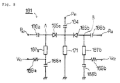
- Fig. 8 shows a known type of high frequency switch using diodes which can constitute the 3-port switches 152 and 153.
- a high frequency switch 161 has first to third ports P61 to P63 corresponding to either the first to third ports P21 to P23 or to the first to third ports P31 to P33.
- the port P61 is connected through a capacitor 164 to a cathode of a diode 165a.
- One end of a distributed constant line 167a is electrically connected to a point A of connection between an anode of the diode 165a and a capacitor 166a. Assuming that the wavelength of a high frequency signal flowing through this switch 161 is ⁇ , the distributed constant line 167a is composed of a transmission line having a length of ⁇ /4 or less.
- the other end of the distributed constant line 167a is connected through a capacitor 168a to ground potential.
- One end of a resistor 169a is connected to a point of connection between the distributed constant line 167a and a capacitor 168a and the other end thereof is connected to a control voltage terminal Vc1.
- the first port P61 is connected through the capacitor 164 to a distributed constant line 171 constructed the same way as the distributed constant line 167a.
- the other end of the distributed constant line 171 is connected to ground potential.
- a diode 165b is connected through the capacitor 164 to the first port P61.
- the anode of the diode 165b is connected through a capacitor 166b to the third port P63.
- a series circuit consisting of a distributed constant line 167b and a capacitor 168b is connected between the anode side of the diode 165b and ground potential.
- One end of a resistor 169b is connected to a point of connection between the distributed constant line 167b and the capacitor 168b and the other end thereof is connected to a control voltage terminal Vc2.
- the high frequency switch 161 by applying different control voltages to the control voltage terminal Vc1 and the second control voltage terminal Vc2, it is possible to realize a state of connection wherein the port P61 is connected to the second port P62 or wherein the port P61 is connected to the third port P63.
- a positive control voltage is applied to the control voltage terminal Vc1 and, on the other hand, a negative control voltage is applied to the control voltage terminal Vc2
- a forward bias voltage is applied to the diode 165a and a reverse bias voltage is applied to the diode 165b.
- the capacitors 166a, 168a, 164, 166b and 168b block the flow of direct current, they block the control current supplied from the control voltage terminal Vc1 which is thereby caused to flow through a circuit portion including the distributed constant line 167a, the diode 165a and the distributed constant line 171. As a result, the diode 165a goes on. On the other hand, a reverse bias voltage is applied to the diode 165b, with the result that the diode 165b goes off.
- the distributed constant line 167a is constructed as mentioned above, one end of the distributed constant line 167a can be set to have ground potential with respect to high frequencies by providing the capacitor 168a with a large capacitance.
- the impedance of a series circuit composed of the distributed constant line 167a and the capacitor 168a as viewed from the connection point A becomes infinite with respect to high frequencies by impedance inversion. Accordingly, a high frequency signal supplied from the second port P62 is caused to flow into the first port P61.
- the distributed constant lines 167a and 167b respectively form the current paths for causing the control currents to flow through the diodes 165a and 165b and perform the function of increasing with respect to high frequency signals the impedances of the distributed constant lines 167a and 167b sides as viewed from the connection points A and B and thereby decreasing the insertion loss and reflection loss.
- the high frequency switch 161 by applying positive and negative control voltages to the control voltage terminals Vc1 and Vc2, it is possible to terminate the connection between the first port P61 and the second port P62 and establish the connection between the first port P61 and the third port P63, and vice versa.
- the switch circuit 151 illustrated in Fig. 7 is constructed using a pair of the high frequency switches 161 as the switches 152 and 153. That is, in the switch circuit 151, two 3-port high frequency switches are used and the first ports thereof are connected to each other.
- the switch circuit 151 is constructed by connecting the two high frequency switches 152 and 153, a high frequency signal passes through the two switches. For example, a transmission output supplied from the transmitter Tx passes through the two switches 153 and 152 before arriving at the antenna ANT. Similarly, a high frequency signal input from the antenna ANT passes through the switches 152 and 153 before being supplied to the receiver Rx. For this reason, it is unavoidable that the insertion loss becomes large and it has been strongly demanded that this insertion loss be reduced. Another problem is that because of the unavoidable increase in insertion loss, it is necessary to increase the transmission output when transmitting, while, on the other hand, a decrease in the gain results when receiving.
- An object of the present invention is to provide a high frequency switch in which the insertion loss is small, the number of the constituent parts can be reduced, and the wiring patterns for supplying the control voltages can be simplified.
- a high frequency switch having first to third ports and enabling changeover between a state of connection between the first and second ports and a state of connection between the first and third ports, comprising a first diode connected between the first and second ports; a second diode connected between the first and third ports, the first and second diodes being connected to the first port in the same direction with respect thereto, coupling capacitors connected between the first port and the first and second diodes, between the second port and the first diode, and between the third port and the second diode; distributed constant lines and capacitors connected in series with each other between the coupling capacitors connected to the first to third ports and reference potentials, and control voltage terminals connected to points of connection between the distributed constant lines and the capacitors; wherein a voltage having a fixed value is applied to the control voltage terminal connected to the point of connection between the distributed constant line and the capacitor connected to the first port.
- a high frequency switch having first to fourth ports and enabling changeover of each of the first and second ports between the third and fourth ports, comprising first to fourth diodes connected between the first and third ports, between the first and fourth ports, between the second and third ports and between the second and fourth ports, the first and second diodes being connected to the first port in the same direction with respect thereto and the third and fourth diodes being connected to the second port in the same direction with respect thereto, distributed constant lines and capacitors connected in series with each other between the third and fourth port sides of the first to fourth diodes and a reference potential, control voltage terminals connected to points of connection between the distributed constant lines and the capacitors, a pair of third distributed constant lines respectively connected between the first and second ports and the reference potential, a capacitor connected between the pair of third distributed constant lines and the reference potential, and a fixed voltage terminal connected to a point of connection between the third distributed constant lines and the capacitor and for having applied thereto a control voltage having a fixed value.
- a high frequency switch having first to fourth ports and enabling changeover of each of the first and second ports between the third and fourth ports, which comprises first to fourth diodes connected between the first and third ports, between the first and fourth ports, between the second and third ports, and between the second and fourth ports, the first and third diodes being connected to the third port in opposite directions and the second and fourth diodes being connected to the fourth port in opposite directions, distributed constant lines and capacitors connected in the series with each other between the first to fourth ports and reference potentials, fixed voltage terminals connected respectively to points of connection between the distributed constant lines and the capacitors in the series circuits composed of the distributed constant lines and capacitors connected to the first and second ports, for applying fixed voltages to the points or connection, and voltage control terminals connected to points of connection between the distributed constant lines and the capacitors in the series circuits composed of the distributed constant lines and capacitors connected to the third and fourth ports.
- a positive power source voltage Vcc for example, can be applied to the control voltage terminal connected to the point of connection between the distributed constant line and the capacitor both connected to the second port, the control voltage terminal connected to the point of connection between the distributed constant line and the capacitor connected to the third port being grounded, and the control voltage terminal connected to the point of connection between the distributed constant line and capacitor connected to the first port being grounded.
- the first diode can be turned “on” and the second diode can be turned “off”. That is, a signal can be caused to flow between the first and second ports by using only one type of power source voltage Vcc.
- a positive power source voltage Vcc for example, can be applied to the control voltage terminal connected to the point of connection between the distributed constant line and capacitor connected to the third port, and each of the remaining control voltage terminals can be grounded.
- Vcc a positive power source voltage
- a voltage having a constant value which is applied to the control voltage terminal connected to the point of connection between the distributed constant line and the capacitor both connected to the first port need not be a positive power source voltage Vcc and may be a negative control voltage -Vcc, or may be grounded.
- This constant voltage is made equal to the control voltage applied to one of the remaining two control voltage terminals and defined as a second voltage, with the control voltage applied to the remaining one control voltage terminal being defined as a first voltage.
- one of the first and second voltages can be set to have ground potential
- a first voltage is applied as the control voltage to the control voltage terminal connected to the point of connection in the series circuit composed of the distributed constant line and the capacitor and connected to the diode desired to be turned “on” so that this diode goes on, and a second voltage different from the first control voltage is applied to each of the remaining control voltage terminals and the fixed voltage terminal.
- one of the first and second voltages can be made to have ground potential, it is sufficient that only one control voltage be provided as in the case of the first aspect of the invention. Accordingly, it is possible to simplify the wiring patterns for supplying the power source voltage and therefore facilitate the design of the wiring patterns for supplying the power source voltage on a printed circuit board or the like, thereby enabling miniaturization of an electronic device as in the case of the first invention.
- the switch circuit 151 when the switch circuit 151 is constructed using the conventional high frequency switches 152 and 153, a high frequency signal passes through two diodes, in the second aspect of the invention a high frequency signal passes through only one diode. Accordingly, the insertion loss can be reduced to 1/2 that in the case where the conventional switch circuit 151 is used, and the service life of the elements constituting the high frequency switch can also be increased.
- the second aspect of the invention when used in a portable telephone, the second aspect of the invention has the effect of reducing the consumption of batteries and enabling long-duration communication by telephone.
- the third aspect of the invention by turning any two of the first to fourth diodes "on” and turning the remaining diodes "off", it is possible to realize a state of connection wherein either the first and third ports or the first and fourth ports are connected to either the second and third ports or the second and fourth forts.
- a first voltage is applied to one of the pair of fixed voltage terminals respectively connected to the first and second ports and a second voltage is applied to the other thereof.
- One of the first and second voltages may be ground potential. Accordingly, each of the above-mentioned states of connection can be realized using only one control voltage.
- the wiring patterns for supplying the power source voltage can be simplified, it is possible to simplify the wiring patterns on a printed circuit board on which the high frequency switch is mounted, thereby enabling promotion of miniaturisation of an electronic device such as a portable telephone in which the high frequency switch is incorporated.
- a high frequency signal passes through only one diode as in the second aspect of the invention. Accordingly, the insertion loss can be reduced to 1/2 compared to the conventional switch circuit 151 using the 3-port high frequency switches 152 and 153. Further, whereas in the conventional switch circuit 151 six transmission lines were needed, in the third aspect of the invention only four transmission lines are needed. Accordingly, from this viewpoint as well, it is possible to achieve miniaturization of an electronic device such as a portable telephone in which the high frequency switch is incorporated.
- a high frequency switch preferably further comprises a distributed constant line and a capacitor connected in series with each other and connected in parallel with at least line of the diodes.
- a parallel resonance circuit is constructed by the capacitance and the impedance of the distributed constant line when this diode is in an "off" state. Accordingly, by making the resonance frequency of this parallel resonance circuit the same as the frequency of the high frequency signal flowing through the switch, it is possible to increase the impedance when the diode is in an "off” state, thereby enabling enhancement of the isolation characteristic.
- the capacitor functions to prevent bypass of a direct current to a circuit portion including the distributed constant line connected in parallel with the diode.
- At least one capacitor is connected between an end of at least one of the diodes and the reference potential.
- at least one capacitor By connecting at least one capacitor between an end of at least one diode and the above-mentioned reference potential, it is possible to adjust the characteristic impedance by this capacitor, thereby enabling a decrease in the insertion loss and the reflection loss. Further, it is possible to shorten the length of the above-mentioned first distributed constant line, thereby contributing to miniaturizing the high frequency switch.
- a resistor is connected in parallel with at least one of the diodes.
- a second resistor is connected in parallel with at least one diode, electric charge accumulated in the capacitance occurring when this diode is in an "off” state is discharged to this resistor simultaneously with changeover thereof to an "on” state.
- Fig. 1 is a circuit diagram illustrating a high frequency switch according to a first embodiment of the invention of this application.
- a high frequency switch 1 is a 3-port high frequency switch having first to third ports P1 to P3.
- a state wherein the first port P1 is connected to the second port P2 can be changed over to a state wherein the first port P1 is connected to the third port P3, and vice versa. That is, in the high frequency switch 1, the same changeover state as in the conventional high frequency switch 161 illustrated in Fig. 8 can be realized.
- cathodes of first and second diodes 3a and 3b are connected through a capacitor 2 to the first port P1.
- An anode of the first diode 3a is connected through a capacitor 4a to the second port P2.
- One end of a distributed constant line 5a is connected to a point A of connection between the anode of the diode 3a and the capacitor 4a.
- the distributed constant line 5a is composed of a stripline, micro-stripline or co-planar guide line having a length of ⁇ /4 or less.
- the other end of the distributed constant line 5a is connected through a capacitor 6a to ground potential.
- a control voltage terminal Vc1 is connected to a point B of connection between the distributed constant line 5a and the capacitor 6a.
- the distributed constant line 5a is a so-called " ⁇ /4 line", it is actually constructed so that it has a length of ⁇ /4 or less as mentioned above because of line inductance and floating capacitance effects.
- control voltage terminal Vc1 may be connected to the point B or connection through a resistor having an appropriate resistance value, whereupon a control voltage supplied to the connection point B can be adjusted.
- the first port P1 is connected through a capacitor 2 to one end of a distributed constant line 7, the other end of which is connected through a capacitor 8 to ground potential.
- the distributed constant line 7 is formed having a length of ⁇ /4 or less.
- a control voltage terminal Vf for receiving a fixed control voltage is connected through a resistor 9 to a point C of connection between the distributed constant line 7 and a capacitor 8.
- An anode of the second diode 3b is connected through a capacitor 4b to the third port P3.
- One end of a distributed constant line 5b is connected to a point D of connection between the anode of the second diode 3b and the capacitor 4b, and the other end thereof is connected through a capacitor 6b to ground potential.
- the distributed constant line 5b is constructed in the same manner as in the case of the distributed constant line 5a, and a control voltage terminal Vc2 is connected to a point E of connection between the distributed constant line 5b and the capacitor 6b.
- the control voltage terminal Vc2 may also be connected through a resistor to the point E of connection.
- a state wherein the first port P1 is connected to the second port P2 can be realized by applying a positive power source voltage +Vcc (first voltage) to the control voltage terminal Vc1 as a control voltage and connecting each of the control voltage terminals Vc2 and Vf to ground potential.
- Vcc first voltage
- a forward bias voltage is applied to the first diode 3a and a reverse bias voltage is applied to the second diode 3b. That is, since each of the capacitors 2, 4a, 6a, 8, 4b and 6b block the flow of direct current therethrough, a control current supplied from the control voltage terminal Vc1 is blocked and flows through a circuit portion including the distributed constant line 5a, the diode 3a, the distributed constant line 7 and the resistor 9, with the result that the diode 3a goes on.
- the potential at the connection point F has a value obtained by subtracting a value corresponding to the voltage reduction in the diode 3a from the voltage Vcc.
- a reverse bias voltage is applied to the diode 3b with the result that the diode 3b goes off.
- one end of the distributed constant line 5a can be set to be at ground potential with respect to high frequencies.
- the impedance of a series circuit composed or the distributed constant line 5a and the capacitor 6a as viewed from the connection point A is infinite with respect to high frequencies as a result of impedance inversion.
- the impedance of the distributed constant line 7 as viewed from the connection point F is also infinite with respect to high frequencies. Accordingly, a high frequency signal flows between the first port P1 and the second port P2.
- connection points D and F since the impedances of the distributed constant lines 5b and 7 as viewed from the connection points D and F are infinite with respect to high frequencies, a high frequency signal does not flow from the connection points D and F toward the distributed constant lines 5b and 7. Accordingly, a high frequency signal flows between the first and third ports P1 and P3.
- the distributed constant lines 5a, 5b and 7 constitute the current paths for allowing the control currents to flow through the diodes 3a and 3b and, at the same time, function to increase the impedance with respect to high frequency signals on the distributed constant line side as viewed from the connection points A, D and F and thereby decrease the insertion loss and reflection loss.
- a power source voltage +Vcc was applied as a first voltage to the first control voltage terminal Vc1 and a voltage of 0V was applied to each of the remaining control voltage terminals Vf and Vc2 in order to connect between the first and second ports P1 and P2 and, on the other hand, a power source voltage +Vcc was applied to the second control voltage terminal Vc2 and a voltage of 0V was applied to each of the remaining control voltage terminals Vc1 and Vf in order to connect between the first and third ports P1 and P3, the method of applying a control voltage is not limited thereto.
- the first and second ports P1 and P2 may be connected to each other.
- the second control voltage terminal Vc2 be grounded so that a voltage of 0V (first voltage) is applied to the second control voltage terminal Vc2 and that, on the other hand, a negative power source voltage -Vcc (second voltage) be applied to each of the remaining control voltage terminals Vc1 and Vf.
- the voltage applied to each of the first and second control voltage terminals Vc1 and Vc2 can be determined in any suitable way such that the diode 3a goes on or off and the diode 3b goes on or off.
- the control voltage terminal Vf in any state of connection between the first and second ports P1 and P2 or between the first and third ports P1 and P3, a fixed voltage is applied thereto.
- the diodes 3a and 3b may be connected with their anode sides connected to the first port P1.
- Table 1 shows a control voltage to each of the control voltage terminals as shown in Table 1 below, it is possible to realize either the connection between the first and second ports P1 and P2 or the connection between the first and third ports P1 and P3.
- capacitors C1 to C3 may be connected between the first to third ports P1 to P3 and the reference potential.
- the capacitance of each of the capacitors C1 to C3 it is possible to compensate for the relevant characteristic impedance, thereby enabling effective decrease in the insertion loss and reflection loss of the high frequency switch 1.
- the high frequency switch 1 in order to realize states of connection between the first and second ports P1 and P2 and between the first and third ports P1 and P3, it is possible to use only one type of control voltage (Vcc or -Vcc) and ground potential. Accordingly, it is sufficient for only one type of power source voltage to he connected to the high frequency switch 1. Thus, it is seen that the wiring patterns for supplying the power source voltage can be simplified.
- Fig. 2 is a circuit diagram illustrating a high frequency switch according to a second embodiment of the present invention.
- the high frequency switch 21 is a 4-port high frequency switch having first to fourth ports P21 to P24.
- the high frequency switch 21 is constructed for establishing a connection between the first and third ports P21 and P23, between the first and fourth ports P21 and P24, between the second and third ports P22 and P23, and between the second and fourth ports P22 and P24.
- either the first or second port P21 or P22 can be connected to either one of the remaining third and fourth ports P23 and P24.
- the antenna ANT is connected to the transmitter Tx or receiver Rx.
- the external terminal EXT may be connected to the transmitter Tx or receiver Rx.
- the switch circuit 151 when the switch circuit 151 is used, a connection can be made between the antenna ANT and the transmitter Tx (for transmission), a connection can be made between the external terminal EXT and the transmitter Tx (for transmission using an external antenna or when the characteristics of the transmitter are measured), and a connection can be made between the external terminal EXT and the receiver Rx (for reception using an external antenna or when the receiving characteristics of the receiver are measured).
- the high frequency switch 21 can be caused to function in the same manner as in the case of the switch circuit 151, by connecting the first and second ports P21 and P22 to the antenna ANT or external terminal EXT respectively and connecting the third and fourth ports P23 and P24 to the transmitter Tx or receiver Rx respectively.
- cathodes of first and second diodes 23 and 24 are connected through a capacitor to the first port P21.
- An anode or the first diode 23 is connected through a capacitor 25 to the third port P23.
- a distributed constant line 26 and a capacitor 27 are connected between a point A of connection between the anode of the first diode 23 and the capacitor 25 and ground potential.
- the distributed constant line 26 is composed of a stripline, a micro-stripline, co-planar guide line or the like, and is a 90° phase shifter or high impedance line having a length of 1/4 of the wavelength ⁇ of a high frequency signal flowing through the high frequency switch 21.
- This distributed constant line 26 is a so-called " ⁇ /4 line".
- the length thereof can be shorter than ⁇ /4 in order to take line inductance and floating capacitance effects into consideration.
- one end of a resistor 28 is connected to a point B of connection between the distributed constant line 26 and the capacitor 27 and the other end thereof is connected to a first control voltage terminal V1.
- resistor 28 is provided in order to adjust the control voltage applied from the control voltage terminal V1 and, therefore, need not always be provided, as indicated by the parentheses in Fig. 2.
- an anode of the second diode 24 is connected through a capacitor 29 to the fourth port P24.
- a distributed constant line 30 constructed in the same manner as the distributed constant line 26 and a capacitor 31 are connected between a point C of connection between the anode of the diode 24 and the capacitor 29, and the ground potential.
- a second control voltage terminal V2 is connected through a resistor 32 to a point D of connection between the distributed constant line 30 and the capacitor 31. This resistor 32 need not always be provided as in the case of the resistor 28.
- the cathodes or third and fourth diodes 43 and 44 are connected through a capacitor 42 to the second port P22.
- the circuit construction between the second and third ports P22 and P23 and the circuit construction between the second and fourth ports P22 and P24 are the same as the circuit construction between the first and third ports P21 and P23 and the first and fourth ports P21 and P24. Accordingly, the corresponding components are denoted by the same reference numerals or symbols.
- a capacitor 45 and a distributed constant line 46 are connected to an anode of the third diode 43. Also, the above-mentioned distributed constant line 46 and a capacitor 47 are connected between a point E of connection between the anode of the diode 43 and the capacitor 45, and the ground potential. A point F of connection between the distributed constant line 46 and the capacitor 47 is connected through a resistor 48 to a third control voltage terminal V3.
- an anode of the fourth diode 44 is connected through a capacitor 49 to the fourth port P24.
- a point G of connection between the anode of the fourth diode 44 and the capacitor 49 is connected to the ground potential through a distributed constant line 50 and a capacitor 51 while, on the other hand, a point H of connection between the distributed constant line 50 and the capacitor 51 is connected through a resistor 52 to the fourth control voltage terminal V4.
- first port P21 and the second port P22 are connected to each other by means of distributed constant lines 61 and 62 and the above-mentioned capacitors 22 and 42.
- Each of the distributed constant lines 61 and 62 is constructed in the same manner as the distributed constant line 26 and a point I of connection therebetween is connected through a capacitor 63 to the ground potential. Also, the point I of connection is connected through a resistor 64 to a fixed voltage terminal Vf.
- the high frequency switch 21 corresponds to a structure comprising two high frequency switches 1 according to the first embodiment which are connected to each other.
- the high frequency switch 21 has the following structure: the first ports P1 or the two high frequency switches 1 are used respectively as the first and second ports P21 and P22 of Fig. 2; the two second ports P2 and two third ports P3 of the two high frequency switches 1 are respectively connected together and are respectively employed as the third and fourth ports P23 and P24 of Fig. 2; and the two control voltage terminals Vf of the two high frequency switches 1 are connected together as the fixed voltage terminal Vf of Fig. 2.
- a positive power source voltage +Vcc is applied as a first voltage to the first control voltage terminal V1.
- the second to fourth control voltage terminals V2 to V4 and the fixed voltage terminal Vf are grounded. Namely, a voltage of 0V is adopted as a second voltage.
- a control current supplied from the control voltage terminal V1 is blocked by the capacitors 22, 25, 27, 29, 31, 42, 45, 47, 49, 51 and 63. Namely, these capacitors impose a limitation on the portion of the circuit where the control current can flow.
- a forward bias voltage is applied to the first diode 23, whereby the first diode 23 goes on.
- a reverse bias voltage is applied to each of the second to fourth diodes 24, 44 and 43, whereby these diodes each go off. Accordingly, a high frequency signal flows between the first and third ports P21 and P23.
- the impedance of a series circuit composed of the distributed constant line 26 and the capacitor 27 becomes infinite with respect to high frequencies. Therefore, a high frequency signal does not flow from the connection point A toward the distributed constant line 26,
- the first state of connection can be realized, whereby a high frequency signal can flow between the first port P1 and the third port P3.
- any one of the second to fourth diodes can be made "on" to thereby realize a state of connection between the first and fourth ports, between the second and third ports, or between the second and fourth ports.
- 0V rather than +Vcc may be adopted as the above-mentioned first control voltage and -Vcc may be adopted as the second voltage.
- the high frequency switch 21 may be constructed with each of the first to fourth diodes in Fig. 2 connected in a direction opposite to that illustrated.
- the same states of connection as mentioned above can be realized by applying the control voltages as shown in Table 3 below.
- a voltage of 0V may be adopted as the first control voltage and a voltage of -Vcc may be adopted as the second voltage.
- the high frequency switch 21 by applying the first voltage to any one of the control voltage terminals V1 to V4 and applying the second voltage to each of the remaining control voltage terminals and to the fixed voltage terminal so that the diode disposed between the ports to be connected to each other goes on and each of the remaining diodes goes off, each of the above-mentioned states of connection can be realized. Since only one diode is "on" when the high frequency switch 21 is operated, the number of the diodes through which a high frequency signal passes is reduced to 1/2 of the corresponding number in the switch circuit 151 using the conventional high frequency switches 152 and 153. Therefore, the insertion loss can be reduced to 1/2 that in the conventional circuit.
- the high frequency switch 21 by using the ground potential as either one or the first and second voltages, it is possible to perform changeover between the states of connection with the use of a single power source voltage alone. Accordingly, the wiring patterns for supplying the power source voltage can be simplified.
- the high frequency switch 21 when the high frequency switch 21 is in operation, only one diode goes an and there is also only bias circuit. Accordingly, it becomes possible to increase the service life of each of the elements constituting the high frequency switch 21. Also, it becomes possible to reduce the consumption of batteries in a portable telephone in which this part is incorporated and, thus, to communicate by telephone for longer periods of time.
- Fig. 3 is a circuit diagram illustrating a high frequency switch 71 according to a third embodiment of the present invention of this application.
- the high frequency switch 71 is a 4-port high frequency switch having first to fourth ports P71 to P74. This switch 71 is constructed for making the connection between the first and third ports P71 and P73; the connection between the second and fourth ports P72 and P74; the connection between the second and third ports P72 and P73; and the connection between the first and fourth ports P71 and P74.
- cathodes of first and second diodes 73 and 74 are connected through a capacitor 72a to the first port P71.
- Anodes or third and fourth diodes 76 and 77 are connected through a capacitor 72b to the second port P72. That is, the diodes 73 and 74 are connected to the first port P71 in the same direction with respect thereto, and the diodes 76 and 77 are connected to the second port P72 in the same direction with respect thereto. Also, the diodes 73 and 76 are connected to the third port P73 in opposite directions and the diodes 74 and 77 are connected to the fourth port P74 in opposite directions to each other.
- a distributed constant line 78a and a capacitor 79a are connected between ground potential and a connection point A between the cathodes of the diodes 73 and 74.
- the point A is connected through a capacitor 72a to the first port P71.
- the distributed constant line 78a is composed of a stripline, a micro-stripline, a co-planar guide line or the like. It is a 90° phase shifter or high impedance line having a length of 1/4 or less of the wavelength ⁇ of a high frequency signal flowing through the high frequency switch 71.
- the distributed constant line naturally constitutes a ⁇ /4 line. However, this line is constructed having a length of 1/4 or less of the wavelength of the high frequency signal, because it is a common practice that that line be formed having a length shorter than ⁇ /4 in order to take the impedance and floating capacitance of the line into consideration.
- a first fixed voltage terminal Vf1 is connected through a resistor 80a to a point B of connection between the distributed constant line 78a and the capacitor 79a.
- three series circuits comprising distributed constant lines 78b, 78c and 78d and capacitors 79b, 79c and 79d are respectively connected to the second to fourth ports P72 to P74 (through respective capacitors 72b, 72c and 72d) and to the ground potential.
- a second fixed voltage terminal Vf2 is connected through a resistor 80b to a point D of connection between the distributed constant line 78b and the capacitor 79b.
- First and second control voltage terminals V1 and V2 are connected through resistors 80c and 80d to points E and F of connection between the distributed constant line 78c and 78d and the capacitors 79c and 79d, respectively.
- resistors 80a to 80d need not always be provided.
- a high frequency signal flows between the first and third ports P71 and P73 and between the second and fourth ports P72 and P74.
- a high frequency signal does not flow from the connection point A toward the distributed constant line 78a.
- a series circuit composed of the distributed constant line 78a and the capacitor 79a is connected between the connection point A and the ground potential, whereby the impedance thereof as viewed from the connection point A side becomes infinite with respect to high frequencies.
- the high frequency signal which flows therethrough passes through a single diode only.
- the high frequency signal which flows between the first port P71 and the third port P73 passes through the diode 73 only.
- a high frequency signal must pass through two diodes, in this embodiment it is sufficient that a high frequency signal passes through only one diode, with the result that the insertion loss can be reduced to 1/2 of that in the conventional case.
- the number of the resistance elements used can be reduced compared to the conventional structure using two high frequency switches 152 and 153, in a case where the high frequency switch 71 is constructed using, for example, a multi-layer substrate, the resulting switch circuit can be reduced in size and cost.
- capacitors C1 to C4 may be connected between the ports P71 to P74 and the ground potential, respectively, as indicated by broken lines. This enables adjustment of the characteristic impedance, a reduction in the insertion loss and reflection loss, and a decrease in length of the distributed constant lines 78a to 78d.
- first and second diodes 73 and 74 and the third and fourth diodes 76 and 77 may he connected in the reverse directions to those illustrated in Fig. 3. In this case as well, it is possible to realize states of connection wherein the first and second ports P71 and P72 are respectively connected to the third and fourth ports P73 and P74, as in the above-mentioned case.
- a discharge resistor 92 is connected in parallel with a diode 91.
- the diode 91 when it is in an "off" state, the diode 91 functions as a capacitor in response to direct current. Accordingly, an electric charge which has been accumulated when the diode 91 is in an "off” state flows simultaneously with the turning-on of the diode.
- the accumulated charge is discharged to the discharge resistor 92, whereby the switching operation from the "off" state to the "on” state of the diode 91 is smoothly performed.
- a distributed constant line 93 and a capacitor connected in series therewith are connected in parallel with the diode 91.
- a parallel resonance circuit is constructed from the capacitance occurring when the diode 91 is "off” and the inductance of the distributed constant line 93. Accordingly, by adjusting the inductance of the distributed constant line 93 so that the resonance frequency of this parallel resonance circuit coincides with the frequency of a high frequency signal to be transmitted, it is possible to increase the impedance when the diode 91 is in an "off” state. As a result, it is possible to increase the isolation characteristic between the two adjacent ports with the diode 91 kept in an "off” state being disposed therebetween.
- the capacitor 94 is provided for the purpose of preventing a direct current from being by-passed due to the distributed constant line 93.
- the distributed constant line 93 can be composed of a stripline, a micro-stripline, a co-planar guide line or the like, the length and impedance thereof are selected so as to cause the resonance frequency of the parallel resonance circuit to coincide with the frequency of a high frequency signal.
- a distributed constant line 93 for forming a parallel resonance circuit is connected in parallel with the diode 91. Also, a capacitor 94 is connected in series with the distributed constant line 93. Further, a capacitor 95 is connected in parallel with the diode 91, and is further connected in parallel with a circuit portion composed of the distributed constant dine 93 and the capacitor 94.
- a parallel resonance circuit can be constructed using a composite capacitance of the capacitance in an "off" state of the diode 91 and the capacitance of the capacitor 95, and the inductance of the distributed constant line 93, whereby it is possible to easily cause the resonance frequency of the parallel resonance circuit to coincide with the frequency of a high frequency signal.
Landscapes
- Waveguide Switches, Polarizers, And Phase Shifters (AREA)
- Transceivers (AREA)
Applications Claiming Priority (2)
| Application Number | Priority Date | Filing Date | Title |
|---|---|---|---|
| JP301105/94 | 1994-12-05 | ||
| JP30110594A JP3196539B2 (ja) | 1994-12-05 | 1994-12-05 | 高周波スイッチ |
Publications (2)
| Publication Number | Publication Date |
|---|---|
| EP0716509A2 true EP0716509A2 (fr) | 1996-06-12 |
| EP0716509A3 EP0716509A3 (fr) | 1998-02-04 |
Family
ID=17892913
Family Applications (1)
| Application Number | Title | Priority Date | Filing Date |
|---|---|---|---|
| EP95119140A Ceased EP0716509A3 (fr) | 1994-12-05 | 1995-12-05 | Commutateur haute fréquence |
Country Status (3)
| Country | Link |
|---|---|
| US (1) | US6518822B1 (fr) |
| EP (1) | EP0716509A3 (fr) |
| JP (1) | JP3196539B2 (fr) |
Families Citing this family (1)
| Publication number | Priority date | Publication date | Assignee | Title |
|---|---|---|---|---|
| JP2002064301A (ja) * | 1999-03-18 | 2002-02-28 | Hitachi Metals Ltd | トリプルバンド用高周波スイッチモジュール |
Citations (6)
| Publication number | Priority date | Publication date | Assignee | Title |
|---|---|---|---|---|
| US3474358A (en) * | 1966-01-18 | 1969-10-21 | Sanders Associates Inc | Multiple-path electronic component |
| DE2652514A1 (de) * | 1976-11-18 | 1978-05-24 | Koerting Radio Werke Gmbh | Hf-quellen-umschalteinrichtung |
| US4542300A (en) * | 1982-08-25 | 1985-09-17 | Dx Antenna Company, Limited | High frequency signal switching device |
| EP0194468A2 (fr) * | 1985-03-05 | 1986-09-17 | Tino Giuseppe Motta | Commutateur de sélection électronique pour la sélection et une éventuelle atténuation des fréquences radio et télévision |
| JPH04140915A (ja) * | 1990-10-02 | 1992-05-14 | Taiyo Yuden Co Ltd | スイッチ回路及びこれを用いた信号減衰回路 |
| EP0508128A2 (fr) * | 1991-03-28 | 1992-10-14 | Texas Instruments Incorporated | Commutateur intégré monolithique à quatre accès avec des diodes PIN en GaAs |
Family Cites Families (6)
| Publication number | Priority date | Publication date | Assignee | Title |
|---|---|---|---|---|
| US3374364A (en) * | 1965-09-22 | 1968-03-19 | Amphenol Corp | Diode transfer switch |
| US3475700A (en) * | 1966-12-30 | 1969-10-28 | Texas Instruments Inc | Monolithic microwave duplexer switch |
| US5170139A (en) * | 1991-03-28 | 1992-12-08 | Texas Instruments Incorporated | PIN diode switch |
| US5507011A (en) * | 1992-12-22 | 1996-04-09 | Murata Manufacturing Co., Ltd. | High-frequency switch including strip line and two switching diodes |
| US5375257A (en) * | 1993-12-06 | 1994-12-20 | Raytheon Company | Microwave switch |
| JP3163918B2 (ja) * | 1994-11-28 | 2001-05-08 | 株式会社村田製作所 | 高周波スイッチ |
-
1994
- 1994-12-05 JP JP30110594A patent/JP3196539B2/ja not_active Expired - Lifetime
-
1995
- 1995-12-04 US US08/567,128 patent/US6518822B1/en not_active Expired - Lifetime
- 1995-12-05 EP EP95119140A patent/EP0716509A3/fr not_active Ceased
Patent Citations (6)
| Publication number | Priority date | Publication date | Assignee | Title |
|---|---|---|---|---|
| US3474358A (en) * | 1966-01-18 | 1969-10-21 | Sanders Associates Inc | Multiple-path electronic component |
| DE2652514A1 (de) * | 1976-11-18 | 1978-05-24 | Koerting Radio Werke Gmbh | Hf-quellen-umschalteinrichtung |
| US4542300A (en) * | 1982-08-25 | 1985-09-17 | Dx Antenna Company, Limited | High frequency signal switching device |
| EP0194468A2 (fr) * | 1985-03-05 | 1986-09-17 | Tino Giuseppe Motta | Commutateur de sélection électronique pour la sélection et une éventuelle atténuation des fréquences radio et télévision |
| JPH04140915A (ja) * | 1990-10-02 | 1992-05-14 | Taiyo Yuden Co Ltd | スイッチ回路及びこれを用いた信号減衰回路 |
| EP0508128A2 (fr) * | 1991-03-28 | 1992-10-14 | Texas Instruments Incorporated | Commutateur intégré monolithique à quatre accès avec des diodes PIN en GaAs |
Also Published As
| Publication number | Publication date |
|---|---|
| JP3196539B2 (ja) | 2001-08-06 |
| US6518822B1 (en) | 2003-02-11 |
| EP0716509A3 (fr) | 1998-02-04 |
| JPH08162802A (ja) | 1996-06-21 |
Similar Documents
| Publication | Publication Date | Title |
|---|---|---|
| US6496083B1 (en) | Diode compensation circuit including two series and one parallel resonance points | |
| EP0756381B1 (fr) | Commutateur haute fréquence | |
| EP0641090B1 (fr) | Commutateur d'antenne | |
| EP1237222B1 (fr) | Etage de transformation à bandes multiples pour dispositif à haute fréquence de commutation multi-bande | |
| US6442376B1 (en) | Composite high frequency component and mobile communication apparatus including the same | |
| US5903178A (en) | Semiconductor integrated circuit | |
| US6072993A (en) | Portable radio transceiver with diplexer-switch circuit for dual frequency band operation | |
| EP1142145B1 (fr) | Module de commutation d'antenne | |
| EP1113519A1 (fr) | Dispositif composite à hautes fréquences | |
| EP0724333B1 (fr) | Commutateur haute fréquence hybride pouvant être utilisé dans un téléphone portable du type à diversité d'antennes | |
| KR101027220B1 (ko) | 다중 모드 라디오 모듈 및 다중 모드 라디오 | |
| US5642083A (en) | High-frequency switch | |
| EP1126624B1 (fr) | Commutateur de radiofréquence | |
| US7027777B2 (en) | High frequency switch and high frequency radio communication apparatus | |
| US6070059A (en) | High-frequency switch | |
| EP0716509A2 (fr) | Commutateur haute fréquence | |
| JP3139351B2 (ja) | 高周波スイッチ | |
| US6529095B1 (en) | Antenna duplexer | |
| JP3168920B2 (ja) | 高周波スイッチ | |
| JP2000124759A (ja) | 可変減衰器及び移動体通信機器 | |
| JP3232928B2 (ja) | 高周波スイッチ | |
| JP3307201B2 (ja) | 高周波スイッチ | |
| GB2375905A (en) | A GSM-DCS dual-band transmit-receive switch for a mobile telephone | |
| JP2001044701A (ja) | 高周波スイッチ回路 |
Legal Events
| Date | Code | Title | Description |
|---|---|---|---|
| PUAI | Public reference made under article 153(3) epc to a published international application that has entered the european phase |
Free format text: ORIGINAL CODE: 0009012 |
|
| AK | Designated contracting states |
Kind code of ref document: A2 Designated state(s): DE FR GB |
|
| PUAL | Search report despatched |
Free format text: ORIGINAL CODE: 0009013 |
|
| AK | Designated contracting states |
Kind code of ref document: A3 Designated state(s): DE FR GB |
|
| 17P | Request for examination filed |
Effective date: 19980227 |
|
| 17Q | First examination report despatched |
Effective date: 19991104 |
|
| STAA | Information on the status of an ep patent application or granted ep patent |
Free format text: STATUS: THE APPLICATION HAS BEEN REFUSED |
|
| 18R | Application refused |
Effective date: 20001207 |