EP0508613A1 - Système à plusieurs puces électroniques et procédé pour alimenter celui-ci en signaux d'horloge - Google Patents
Système à plusieurs puces électroniques et procédé pour alimenter celui-ci en signaux d'horloge Download PDFInfo
- Publication number
- EP0508613A1 EP0508613A1 EP92302223A EP92302223A EP0508613A1 EP 0508613 A1 EP0508613 A1 EP 0508613A1 EP 92302223 A EP92302223 A EP 92302223A EP 92302223 A EP92302223 A EP 92302223A EP 0508613 A1 EP0508613 A1 EP 0508613A1
- Authority
- EP
- European Patent Office
- Prior art keywords
- semiconductor chips
- clock signal
- signal
- light
- accordance
- Prior art date
- Legal status (The legal status is an assumption and is not a legal conclusion. Google has not performed a legal analysis and makes no representation as to the accuracy of the status listed.)
- Granted
Links
Images




Classifications
-
- H—ELECTRICITY
- H04—ELECTRIC COMMUNICATION TECHNIQUE
- H04B—TRANSMISSION
- H04B10/00—Transmission systems employing electromagnetic waves other than radio-waves, e.g. infrared, visible or ultraviolet light, or employing corpuscular radiation, e.g. quantum communication
- H04B10/80—Optical aspects relating to the use of optical transmission for specific applications, not provided for in groups H04B10/03 - H04B10/70, e.g. optical power feeding or optical transmission through water
- H04B10/801—Optical aspects relating to the use of optical transmission for specific applications, not provided for in groups H04B10/03 - H04B10/70, e.g. optical power feeding or optical transmission through water using optical interconnects, e.g. light coupled isolators, circuit board interconnections
-
- G—PHYSICS
- G02—OPTICS
- G02B—OPTICAL ELEMENTS, SYSTEMS OR APPARATUS
- G02B6/00—Light guides; Structural details of arrangements comprising light guides and other optical elements, e.g. couplings
- G02B6/24—Coupling light guides
- G02B6/42—Coupling light guides with opto-electronic elements
- G02B6/4201—Packages, e.g. shape, construction, internal or external details
- G02B6/4204—Packages, e.g. shape, construction, internal or external details the coupling comprising intermediate optical elements, e.g. lenses, holograms
- G02B6/421—Packages, e.g. shape, construction, internal or external details the coupling comprising intermediate optical elements, e.g. lenses, holograms the intermediate optical component consisting of a short length of fibre, e.g. fibre stub
-
- G—PHYSICS
- G02—OPTICS
- G02B—OPTICAL ELEMENTS, SYSTEMS OR APPARATUS
- G02B6/00—Light guides; Structural details of arrangements comprising light guides and other optical elements, e.g. couplings
- G02B6/24—Coupling light guides
- G02B6/42—Coupling light guides with opto-electronic elements
- G02B6/4201—Packages, e.g. shape, construction, internal or external details
- G02B6/4249—Packages, e.g. shape, construction, internal or external details comprising arrays of active devices and fibres
-
- G—PHYSICS
- G02—OPTICS
- G02B—OPTICAL ELEMENTS, SYSTEMS OR APPARATUS
- G02B6/00—Light guides; Structural details of arrangements comprising light guides and other optical elements, e.g. couplings
- G02B6/24—Coupling light guides
- G02B6/42—Coupling light guides with opto-electronic elements
- G02B6/43—Arrangements comprising a plurality of opto-electronic elements and associated optical interconnections
-
- G—PHYSICS
- G06—COMPUTING OR CALCULATING; COUNTING
- G06F—ELECTRIC DIGITAL DATA PROCESSING
- G06F1/00—Details not covered by groups G06F3/00 - G06F13/00 and G06F21/00
- G06F1/04—Generating or distributing clock signals or signals derived directly therefrom
- G06F1/10—Distribution of clock signals, e.g. skew
- G06F1/105—Distribution of clock signals, e.g. skew in which the distribution is at least partially optical
-
- H—ELECTRICITY
- H05—ELECTRIC TECHNIQUES NOT OTHERWISE PROVIDED FOR
- H05K—PRINTED CIRCUITS; CASINGS OR CONSTRUCTIONAL DETAILS OF ELECTRIC APPARATUS; MANUFACTURE OF ASSEMBLAGES OF ELECTRICAL COMPONENTS
- H05K1/00—Printed circuits
- H05K1/02—Details
- H05K1/0274—Optical details, e.g. printed circuits comprising integral optical means
-
- H—ELECTRICITY
- H05—ELECTRIC TECHNIQUES NOT OTHERWISE PROVIDED FOR
- H05K—PRINTED CIRCUITS; CASINGS OR CONSTRUCTIONAL DETAILS OF ELECTRIC APPARATUS; MANUFACTURE OF ASSEMBLAGES OF ELECTRICAL COMPONENTS
- H05K1/00—Printed circuits
- H05K1/18—Printed circuits structurally associated with non-printed electric components
- H05K1/181—Printed circuits structurally associated with non-printed electric components associated with surface mounted components
Definitions
- the present invention relates to a multichip system in which a plurality of semiconductor chips are synchronously operated based on a clock signal from a clock signal supply unit, and to a method of supplying the clock signal therefor.
- Fig. 14 is a block diagram of a conventional multichip system.
- a plurality of semiconductor chips 1 are provided on a printed circuit board 2.
- Aluminium wires 3 on the printed circuit board 2 electrically connect the respective semiconductor chips 1 to a clock signal supply unit 4.
- all the semiconductor chips 1 are operated in synchronism with each other based on a clock signal S CL given from the clock signal supply unit 4 through the aluminium wires 3.
- the aluminium wires 3 act as a transmission path for the clock signal S CL .
- the lengths of the aluminium wires 3, i.e., transmission distances between the clock signal supply unit 4 and the semiconductor chips 1 are different from each other. Accordingly, periods of time required to transmit the clock signal S CL from the clock signal supply unit 4 to the respective semiconductor chips 1 (hereinafter referred to as "signal transmission time") are different depending on the transmission distance.
- clock skew occurs because of the different lengths of the aluminium wires 3.
- the impedance of the aluminium wires 3 increases as the frequency of the clock signal S CL grows higher. In this case, there has been a practically serious problem that the clock skew is resultingly aggravated as compared with the clock signal S CL having a low frequency.
- the present invention is directed to a multichip system, (a) a clock signal supply unit for generating a clock signal, the clock signal being an electric signal; (b) a light emitting unit blinking in response to the clock signal from the clock signal supply unit, to thereby transform the clock signal into a light signal corresponding to the clock signal; and (c) a plurality of semiconductor chips each of which includes (c-1) a semiconductor element having an internal circuit, (c-2) a photodetector for transforming the light signal back into an electric signal, the photodetector being electrically connected to the internal circuit such that the electric signal is supplied to the internal circuit, the electric signal serving as a clock signal for the internal circuit, and (c-3) a light transmission unit for receiving the light signal from the light emitting unit to transmit the light signal to the photodetector.
- the present invention is also directed to a method of supplying a clock signal for a multichip system, the multichip system including a plurality of semiconductor chips each of which has an internal circuit as function of the clock signal.
- the method comprises the steps of; generating the clock signal; transforming the clock signal into a light signal; transmitting the light signal to internal portions of the semiconductor chips to transform the light signal back into an electric signal; and supplying the electric signal to the internal circuits, whereby all of the internal circuits are synchronously operated based on the electric signal.
- the light emitting device blinks based on the clock signal from the clock signal supply unit, whereby the clock signal (electric signal) is transformed into the light signal.
- the photodetector included in the semiconductor chip receives the light from the light emitting device, transforms the light signal from the light emitting device into the electric signal, and supplies the signal as the clock signal to the internal circuit of the semiconductor chip. Clock skew caused by the impedance of aluminium wires is eliminated.
- the periods of signal transmission time for supplying the clock signal to the respective semiconductor chips are precisely equal or very close to equal.
- an object of the present invention is to provide a multichip system capable of suppressing clock skew.
- Another object of the present invention is to provide a method of supplying a clock signal capable of suppressing clock skew.
- Fig. 1A shows a multichip system according to a first preferred embodiment of the present invention.
- a plurality of semiconductor chips 10A and a clock signal supply unit 4 are mounted on a printed circuit board 2.
- a case member 21 is installed on the printed circuit board 2 such that it encloses the semiconductor chips 10A and the clock signal supply unit 4, whereby an IC housing box 20 is formed.
- the clock signal supply unit 4 which is composed of a single semiconductor chip or a plurality of circuit components, outputs a clock signal S CL for synchronously operating internal circuits (not shown) of the semiconductor chips 10A.
- An LED (light emitting diode) 30 is fitted to an inner peripheral face 21a of the IC housing box 20, the face 21a directed toward the printed circuit board 2.
- the clock signal (electric signal) S CL is transmitted from the clock signal supply unit 4 through a conductor 31 to the LED 30, the LED 30 blinks in response to the clock signal.
- the clock signal (electric signal) S CL from the clock signal supply unit 4 is thus transformed into a light signal.
- Fig. 2 is a top plan view of the semiconductor chip 10A
- Fig. 3 is a cross-sectional view taken along the line A - A' of Fig. 2.
- a semiconductor element 11 including the internal circuit is mounted on a die bonding pad 12 and is electrically connected to leads 14 through Au wires 13.
- the semiconductor element 11, the die pad 12, the Au wires 13, and parts of the leads 14 are sealed in a mold resin 15.
- An optical element for introducing light coming from above into the semiconductor chip 10A e.g., a lens 16 is fitted to the top face of the semiconductor chip 10A.
- the light passing through the lens 16 is adapted to be introduced through a hollow 17 to a photodetector 11a provided on an upper portion of the semiconductor element 11.
- the lens 16 and the hollow 17 serve as light transmission means for transmitting the light signal from the LED 30 to the interior of the semiconductor chip 10A.
- the light signal emitted from the LED 30 in response to the clock signal S CL enters the photodetector 11a through the lens 16 and hollow 17 and is transformed back into a clock signal (electric signal).
- the clock signal from the clock signal supply unit 4 is thus supplied to the internal circuit of the semiconductor element 11.
- the hollow 17 may be replaced with an optical fiber through which the light passing through the lens 16 enters the photodetector 11a.
- the LED 30 transforms the clock signal (electric signal) S CL into the light signal
- the photodetectors 11a of the respective semiconductor chips 10A transform the light signal back into the electric signal.
- the electric signal is supplied to the internal circuits of the semiconductor devices 11 as the clock signal, so that the respective semiconductor chips 10A are operated in synchronism with each other.
- clock skew resulting from the impedance of aluminium wires is eliminated.
- the periods of signal transmission time, for transmitting the clock signal S CL from the clock signal supply unit 4 to the respective semiconductor chips 10A are substantially equal.
- the first preferred embodiment employs the semiconductor chip 10A in which the photodetector 11a and the semiconductor element 11 are formed integrally.
- a semiconductor chip 10B of Fig. 4 may be employed.
- the semiconductor chip 10B comprises a semiconductor element 11 and a photodetector 11a which are separately formed and which are then connected to each other within the same package.
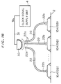
- Fig. 1B it is also applicable to make optical connections between the LED 30 and the respective semiconductor chips 10A (or 10B) through optical fibers 22 serving as a light transmission path.
- the light signal from the LED 30 enters inlet ends 22a of the optical fibers 22, the light signal is transmitted through the optical fibers 22 and is emitted from outlet ends 22b thereof toward the top faces of the semiconductor chips 10A.
- Fig. 5A shows the multichip system according to a second preferred embodiment of the present invention.
- the LED 30 provided on a center portion of the printed circuit board 2 is electrically connected to the clock signal supply unit 4 mounted on the printed circuit board 2 through a printed wiring 32.
- the clock signal (electric signal) S CL is transmitted from the clock signal supply unit 4 through the printed wiring 32 to the LED 30, the LED 30 blinks in response to the clock signal S CL , so that the light signal responsive to the clock signal S CL is emitted radially.
- Fig. 6 is a front elevation of the semiconductor chip 10C
- Fig. 7 is a cross-sectional view taken along the line B - B' of Fig. 6.
- the semiconductor chip 10C has substantially the same structure as the semiconductor chip 10A of Fig. 3 except the following difference:
- the lens 16 serving as the optical element for receiving the external light signal is mounted on the top face thereof.
- the lens 16 is mounted on a side face thereof. Referring to Fig.
- the lens 16 serves as the light transmission means in cooperation with an optical fiber 17'.
- the light passing through the lens 16 enters the photodetector 11a of the semiconductor element 11 through the optical fiber 17'.
- the light signal emitted from the LED 30 in response to the clock signal S CL enters the photodetector 11a and is transformed back into the clock signal (electric signal).
- the clock signal is supplied to the internal circuit (not shown) of the semiconductor element 11.
- the lens 16 may be replaced with a transparent plate.
- the light signal from the LED 30, corresponding to the clock signal output from the clock signal supply unit 4 is transmitted to the respective semiconductor chips 10C and is transformed back into the electric signal. Thereafter, the transformed electric signal is supplied to the internal circuits of the semiconductor devices 11 as the clock signal.
- the second preferred embodiment has the effects similar to the first preferred embodiment.
- the second preferred embodiment employs the semiconductor chip 10C in which the photodetector 11a and the semiconductor element 11 are formed integrally.
- a semiconductor chip 10D of Fig. 8, however, may be employed which is comprised of a semiconductor element 11 and a photodetector 11a separately formed.
- the light passing through the lens 16 is adapted to enter the photodetector 11a through the optical fiber 17' or through the hollow.
- Fig. 5B it is also applicable to make optical connections between the LED 30 and the respective semiconductor chips 10C (or 10D) through the optical fibers 22.
- the light signal from the LED 30 is directly applied to the lenses 16 fitted to the side faces of the respective semiconductor chips 10C (or 10D) through the optical fibers 22.
- Fig. 9 shows the multichip system according to a third preferred embodiment of the present invention.
- the LED 30, fixed to the printed circuit board 2 by a LED supporting member 33 is electrically connected to the clock signal supply unit 4 mounted on the printed circuit board 2 through the conductor 31.
- the clock signal (electric signal) S CL is applied from the clock signal supply unit 4 through the conductor 31 to the LED 30, the LED 30 blinks in response to the clock signal S CL , to thereby generate a light signal corresponding to the clock signal S CL .
- the light signal is emitted toward the surface of the printed circuit board 2.
- a plurality of optical fibers 22 are buried in the printed circuit board 2.
- the light signal from the LED 30 is transmitted to predetermined positions by the optical fibers 22 and, thereafter, is emitted upwardly from the surface of the printed circuit board 2.
- a plurality of semiconductor chips 10E are mounted on the printed circuit board 2 such that the lenses 16 described later are in the positions of the outlet ends of the optical fibers 22.
- Fig. 10 is a top plan view of the semiconductor chip 10E
- Fig. 11 is a cross-sectional view taken along the line C - C' of Fig. 10.
- the semiconductor chip 10E has substantially the same structure as the semiconductor chip 10A of Fig. 3 except the following difference:
- the lens 16 serving as the optical element for receiving the external light signal is mounted on the top face of the chip.
- the lens 16 is mounted on the bottom face of the chip.
- the lens 16 and the optical fiber 17' cooperate to light transmission means for transmitting the external light signal to the semiconductor element 11, as shown in Fig. 11: more precisely, the light passing through the lens 16 is transmitted through the optical fiber 17' to the photodetector 11a of the semiconductor element 11. The light signal is transformed back into the clock signal (electric signal). The clock signal is supplied to the internal circuit (not shown) of the semiconductor element 11.
- the lens 16 may be replaced with the transparent plate.
- the LED 30 transforms the clock signal (electric signal) S CL into the light signal
- the photodetectors 11a of the respective semiconductor chips 10E transform the light signal back into the electric signal, in the third preferred embodiment.
- the transformed electric signal is, as the clock signal, supplied to the internal circuits of the semiconductor devices 11.
- the third preferred embodiment has the effects similar to the first preferred embodiment.
- the third preferred embodiment employs the semiconductor chip 10E in which the photodetector 11a and the semiconductor element 11 are formed integrally.
- a semiconductor chip 10F of Fig. 12, however, may be employed which includes two components (a semiconductor element 11 and a photodetector 11a) separately formed. In this case, the light passing through the lens 16 is adapted to enter the photodetector 11a through the optical fiber 17' or through the hollow.
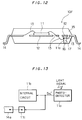
- a lead 14a in the semiconductor chip enables a clock signal S CL ', supplied to an internal circuit 11b of the semiconductor element 11, to be monitored.
- the semiconductor element 11 is equipped with a bonding pad 11c for monitoring.
- the signal S CL ' from the photodetector 11a is applied not only to the internal circuit 11b of the semiconductor element 11 but also to the bonding pad 11c.
- the clock signal S CL ' can be monitored through the Au wires 13 and the lead 14a.
- the first to third preferred embodiments employ the lens 16 as the optical element.
- the lens 16 may be replaced with the transparent plate.
Landscapes
- Physics & Mathematics (AREA)
- General Physics & Mathematics (AREA)
- Optics & Photonics (AREA)
- Engineering & Computer Science (AREA)
- Theoretical Computer Science (AREA)
- General Engineering & Computer Science (AREA)
- Electromagnetism (AREA)
- Computer Networks & Wireless Communication (AREA)
- Signal Processing (AREA)
- Optical Couplings Of Light Guides (AREA)
- Led Device Packages (AREA)
- Optical Communication System (AREA)
Applications Claiming Priority (4)
| Application Number | Priority Date | Filing Date | Title |
|---|---|---|---|
| JP74858/91 | 1991-04-08 | ||
| JP3074858A JPH04313269A (ja) | 1991-04-08 | 1991-04-08 | マルチチップシステム及びマルチチップシステムにおけるクロック信号供給方法 |
| JP86834/91 | 1991-04-18 | ||
| JP3086834A JPH04320073A (ja) | 1991-04-18 | 1991-04-18 | マルチチップシステムにおけるクロック信号供給方法 |
Publications (2)
| Publication Number | Publication Date |
|---|---|
| EP0508613A1 true EP0508613A1 (fr) | 1992-10-14 |
| EP0508613B1 EP0508613B1 (fr) | 1996-09-04 |
Family
ID=26416031
Family Applications (1)
| Application Number | Title | Priority Date | Filing Date |
|---|---|---|---|
| EP92302223A Expired - Lifetime EP0508613B1 (fr) | 1991-04-08 | 1992-03-16 | Système à plusieurs puces électroniques et procédé pour alimenter celui-ci en signaux d'horloge |
Country Status (3)
| Country | Link |
|---|---|
| US (1) | US5250816A (fr) |
| EP (1) | EP0508613B1 (fr) |
| DE (1) | DE69213294T2 (fr) |
Cited By (3)
| Publication number | Priority date | Publication date | Assignee | Title |
|---|---|---|---|---|
| EP0588746A1 (fr) * | 1992-09-16 | 1994-03-23 | International Business Machines Corporation | Méthode de synchronisation pour circuits intégrés |
| GB2326277A (en) * | 1997-06-11 | 1998-12-16 | Lsi Logic Corp | Low skew signal distribution for integrated circuits |
| GB2340995A (en) * | 1998-08-26 | 2000-03-01 | Lsi Logic Corp | Low skew signal distribution for integrated circuits |
Families Citing this family (8)
| Publication number | Priority date | Publication date | Assignee | Title |
|---|---|---|---|---|
| US5414293A (en) * | 1992-10-14 | 1995-05-09 | International Business Machines Corporation | Encapsulated light emitting diodes |
| US5516727A (en) * | 1993-04-19 | 1996-05-14 | International Business Machines Corporation | Method for encapsulating light emitting diodes |
| US5822106A (en) * | 1996-12-30 | 1998-10-13 | Lucent Technologies Inc. | Synchronization of digital systems using optical pulses and mdoulators |
| JP2001148485A (ja) * | 1999-09-06 | 2001-05-29 | Seiko Epson Corp | 半導体装置 |
| US6807352B2 (en) * | 2001-02-11 | 2004-10-19 | Georgia Tech Research Corporation | Optical waveguides with embedded air-gap cladding layer and methods of fabrication thereof |
| US6785458B2 (en) * | 2001-02-11 | 2004-08-31 | Georgia Tech Research Corporation | Guided-wave optical interconnections embedded within a microelectronic wafer-level batch package |
| US7016569B2 (en) * | 2002-07-31 | 2006-03-21 | Georgia Tech Research Corporation | Back-side-of-die, through-wafer guided-wave optical clock distribution networks, method of fabrication thereof, and uses thereof |
| TWI260788B (en) * | 2004-10-06 | 2006-08-21 | Siliconware Precision Industries Co Ltd | Electronic package including light emitter and IC |
Citations (6)
| Publication number | Priority date | Publication date | Assignee | Title |
|---|---|---|---|---|
| EP0033631A2 (fr) * | 1980-02-05 | 1981-08-12 | The Marconi Company Limited | Arrangements pour processeur |
| WO1985003179A1 (fr) * | 1984-01-09 | 1985-07-18 | Hase Klaus Ruediger | Circuit avec bus optique |
| EP0159832A2 (fr) * | 1984-04-14 | 1985-10-30 | Stc Plc | Interconnexion de circuits intégrés |
| EP0335104A2 (fr) * | 1988-03-31 | 1989-10-04 | Siemens Aktiengesellschaft | Dispositif pour relier optiquement un ou plusieurs émetteurs optiques d'un ou plusieurs circuits intégrés |
| US4890895A (en) * | 1987-11-13 | 1990-01-02 | Kopin Corporation | Optoelectronic interconnections for III-V devices on silicon |
| US4961616A (en) * | 1989-07-13 | 1990-10-09 | Mitsubishi Denki Kabushiki Kaisha | Optical semiconductor device |
Family Cites Families (4)
| Publication number | Priority date | Publication date | Assignee | Title |
|---|---|---|---|---|
| US3631251A (en) * | 1970-02-26 | 1971-12-28 | Kurt Lehovec | Array comprising row of electro-optical elements and associated row of semiconducting microcircuits located on adjoining faces of a parallelepipedal slab |
| US4675624A (en) * | 1985-03-29 | 1987-06-23 | Rca Corporation | Electrical phase shifter controlled by light |
| US4899204A (en) * | 1987-12-01 | 1990-02-06 | General Electric Company | High voltage switch structure with light responsive diode stack |
| US5093879A (en) * | 1990-06-22 | 1992-03-03 | International Business Machines Corporation | Electro-optical connectors |
-
1992
- 1992-01-24 US US07/824,982 patent/US5250816A/en not_active Expired - Fee Related
- 1992-03-16 DE DE69213294T patent/DE69213294T2/de not_active Expired - Fee Related
- 1992-03-16 EP EP92302223A patent/EP0508613B1/fr not_active Expired - Lifetime
Patent Citations (6)
| Publication number | Priority date | Publication date | Assignee | Title |
|---|---|---|---|---|
| EP0033631A2 (fr) * | 1980-02-05 | 1981-08-12 | The Marconi Company Limited | Arrangements pour processeur |
| WO1985003179A1 (fr) * | 1984-01-09 | 1985-07-18 | Hase Klaus Ruediger | Circuit avec bus optique |
| EP0159832A2 (fr) * | 1984-04-14 | 1985-10-30 | Stc Plc | Interconnexion de circuits intégrés |
| US4890895A (en) * | 1987-11-13 | 1990-01-02 | Kopin Corporation | Optoelectronic interconnections for III-V devices on silicon |
| EP0335104A2 (fr) * | 1988-03-31 | 1989-10-04 | Siemens Aktiengesellschaft | Dispositif pour relier optiquement un ou plusieurs émetteurs optiques d'un ou plusieurs circuits intégrés |
| US4961616A (en) * | 1989-07-13 | 1990-10-09 | Mitsubishi Denki Kabushiki Kaisha | Optical semiconductor device |
Non-Patent Citations (4)
| Title |
|---|
| IBM TECHNICAL DISCLOSURE BULLETIN vol. 26, no. 4, September 1983, pages 1793-1796; L. BALLIET et al.: "Optical Transmission System for Interconnecting Electronic Units" * |
| OPTICAL ENGINEERING vol. 25, no. 10, October 1986, pages 1086-1102, Bellingham, WA, US; D.H. HARTMAN: "Digital high speed interconnects: a study of the optical alternative" * |
| OPTICAL ENGINEERING vol. 25, no. 10, October 1986, pages 1103-1108, Bellingham, WA,US; B.D. CLYMER et al.: "Optical clock distribution to silicon chips" * |
| OPTICAL ENGINEERING vol. 25, no. 10, October 1986, pages 1109-1118, Bellingham, WA, US; L.A. BERGMAN: "Holographic optical interconnects for VLST" * |
Cited By (6)
| Publication number | Priority date | Publication date | Assignee | Title |
|---|---|---|---|---|
| EP0588746A1 (fr) * | 1992-09-16 | 1994-03-23 | International Business Machines Corporation | Méthode de synchronisation pour circuits intégrés |
| US5430567A (en) * | 1992-09-16 | 1995-07-04 | International Business Machines Corporation | Method of clocking integrated circuit chips |
| US5434524A (en) * | 1992-09-16 | 1995-07-18 | International Business Machines Corporation | Method of clocking integrated circuit chips |
| GB2326277A (en) * | 1997-06-11 | 1998-12-16 | Lsi Logic Corp | Low skew signal distribution for integrated circuits |
| GB2340995A (en) * | 1998-08-26 | 2000-03-01 | Lsi Logic Corp | Low skew signal distribution for integrated circuits |
| US6624447B1 (en) | 1998-08-26 | 2003-09-23 | Lsi Logic Corporation | Low skew signal distribution for integrated circuits |
Also Published As
| Publication number | Publication date |
|---|---|
| DE69213294T2 (de) | 1997-04-10 |
| DE69213294D1 (de) | 1996-10-10 |
| US5250816A (en) | 1993-10-05 |
| EP0508613B1 (fr) | 1996-09-04 |
Similar Documents
| Publication | Publication Date | Title |
|---|---|---|
| US5122893A (en) | Bi-directional optical transceiver | |
| US4695120A (en) | Optic-coupled integrated circuits | |
| EP0314651B1 (fr) | Convertisseur électro-optique | |
| US6752539B2 (en) | Apparatus and system for providing optical bus interprocessor interconnection | |
| US6583902B1 (en) | Modular fiber-optic transceiver | |
| US9057850B2 (en) | Optoelectronic module | |
| EP0437931B1 (fr) | Boîtier pour couple de dispositifs optiques | |
| US6955481B2 (en) | Method and apparatus for providing parallel optoelectronic communication with an electronic device | |
| US5280191A (en) | Lightwave packaging for pairs of optical devices having thermal dissipation means | |
| EP0510860A2 (fr) | Agencement d'un boîtier optique moulé | |
| EP0381370A2 (fr) | Techniques d'emballage pour transmetteurs/récepteurs optiques | |
| EP0508613B1 (fr) | Système à plusieurs puces électroniques et procédé pour alimenter celui-ci en signaux d'horloge | |
| US6940155B2 (en) | IC package, optical transmitter, and optical receiver | |
| US8457454B1 (en) | Optical substrate chip carrier | |
| US6592269B1 (en) | Apparatus and method for integrating an optical transceiver with a surface mount package | |
| US20140071632A1 (en) | Semiconductor device, communication device, and semiconductor package | |
| CN217587682U (zh) | 一种光模块 | |
| US7217957B2 (en) | Optical transmission module | |
| US7226216B2 (en) | Optoelectronic transmission and/or reception arrangement | |
| JPH0832106A (ja) | 光半導体装置及び基板実装装置 | |
| US6380563B2 (en) | Opto-electric mounting apparatus | |
| CN217034337U (zh) | 一种光模块 | |
| JPH04313269A (ja) | マルチチップシステム及びマルチチップシステムにおけるクロック信号供給方法 | |
| JP3952611B2 (ja) | 光電変換装置 | |
| JPH11202163A (ja) | 光リンク装置 |
Legal Events
| Date | Code | Title | Description |
|---|---|---|---|
| PUAI | Public reference made under article 153(3) epc to a published international application that has entered the european phase |
Free format text: ORIGINAL CODE: 0009012 |
|
| AK | Designated contracting states |
Kind code of ref document: A1 Designated state(s): DE FR GB |
|
| 17P | Request for examination filed |
Effective date: 19930114 |
|
| 17Q | First examination report despatched |
Effective date: 19950316 |
|
| GRAH | Despatch of communication of intention to grant a patent |
Free format text: ORIGINAL CODE: EPIDOS IGRA |
|
| GRAA | (expected) grant |
Free format text: ORIGINAL CODE: 0009210 |
|
| GRAH | Despatch of communication of intention to grant a patent |
Free format text: ORIGINAL CODE: EPIDOS IGRA |
|
| AK | Designated contracting states |
Kind code of ref document: B1 Designated state(s): DE FR GB |
|
| REF | Corresponds to: |
Ref document number: 69213294 Country of ref document: DE Date of ref document: 19961010 |
|
| REG | Reference to a national code |
Ref country code: GB Ref legal event code: 727 |
|
| REG | Reference to a national code |
Ref country code: GB Ref legal event code: 727A |
|
| ET | Fr: translation filed | ||
| REG | Reference to a national code |
Ref country code: GB Ref legal event code: 727B |
|
| REG | Reference to a national code |
Ref country code: GB Ref legal event code: SP |
|
| PLBE | No opposition filed within time limit |
Free format text: ORIGINAL CODE: 0009261 |
|
| STAA | Information on the status of an ep patent application or granted ep patent |
Free format text: STATUS: NO OPPOSITION FILED WITHIN TIME LIMIT |
|
| 26N | No opposition filed | ||
| PGFP | Annual fee paid to national office [announced via postgrant information from national office to epo] |
Ref country code: FR Payment date: 20000310 Year of fee payment: 9 |
|
| PGFP | Annual fee paid to national office [announced via postgrant information from national office to epo] |
Ref country code: DE Payment date: 20000313 Year of fee payment: 9 |
|
| PGFP | Annual fee paid to national office [announced via postgrant information from national office to epo] |
Ref country code: GB Payment date: 20000315 Year of fee payment: 9 |
|
| PG25 | Lapsed in a contracting state [announced via postgrant information from national office to epo] |
Ref country code: GB Free format text: LAPSE BECAUSE OF NON-PAYMENT OF DUE FEES Effective date: 20010316 |
|
| GBPC | Gb: european patent ceased through non-payment of renewal fee |
Effective date: 20010316 |
|
| PG25 | Lapsed in a contracting state [announced via postgrant information from national office to epo] |
Ref country code: FR Free format text: LAPSE BECAUSE OF NON-PAYMENT OF DUE FEES Effective date: 20011130 |
|
| REG | Reference to a national code |
Ref country code: FR Ref legal event code: ST |
|
| PG25 | Lapsed in a contracting state [announced via postgrant information from national office to epo] |
Ref country code: DE Free format text: LAPSE BECAUSE OF NON-PAYMENT OF DUE FEES Effective date: 20020101 |