EP0335104A2 - Dispositif pour relier optiquement un ou plusieurs émetteurs optiques d'un ou plusieurs circuits intégrés - Google Patents
Dispositif pour relier optiquement un ou plusieurs émetteurs optiques d'un ou plusieurs circuits intégrés Download PDFInfo
- Publication number
- EP0335104A2 EP0335104A2 EP89103004A EP89103004A EP0335104A2 EP 0335104 A2 EP0335104 A2 EP 0335104A2 EP 89103004 A EP89103004 A EP 89103004A EP 89103004 A EP89103004 A EP 89103004A EP 0335104 A2 EP0335104 A2 EP 0335104A2
- Authority
- EP
- European Patent Office
- Prior art keywords
- optical
- wst
- spacer
- light
- waveguide
- Prior art date
- Legal status (The legal status is an assumption and is not a legal conclusion. Google has not performed a legal analysis and makes no representation as to the accuracy of the status listed.)
- Withdrawn
Links
Images

Classifications
-
- G—PHYSICS
- G02—OPTICS
- G02B—OPTICAL ELEMENTS, SYSTEMS OR APPARATUS
- G02B6/00—Light guides; Structural details of arrangements comprising light guides and other optical elements, e.g. couplings
- G02B6/24—Coupling light guides
- G02B6/42—Coupling light guides with opto-electronic elements
- G02B6/43—Arrangements comprising a plurality of opto-electronic elements and associated optical interconnections
-
- H—ELECTRICITY
- H04—ELECTRIC COMMUNICATION TECHNIQUE
- H04B—TRANSMISSION
- H04B10/00—Transmission systems employing electromagnetic waves other than radio-waves, e.g. infrared, visible or ultraviolet light, or employing corpuscular radiation, e.g. quantum communication
- H04B10/80—Optical aspects relating to the use of optical transmission for specific applications, not provided for in groups H04B10/03 - H04B10/70, e.g. optical power feeding or optical transmission through water
- H04B10/801—Optical aspects relating to the use of optical transmission for specific applications, not provided for in groups H04B10/03 - H04B10/70, e.g. optical power feeding or optical transmission through water using optical interconnects, e.g. light coupled isolators, circuit board interconnections
-
- H—ELECTRICITY
- H10—SEMICONDUCTOR DEVICES; ELECTRIC SOLID-STATE DEVICES NOT OTHERWISE PROVIDED FOR
- H10W—GENERIC PACKAGES, INTERCONNECTIONS, CONNECTORS OR OTHER CONSTRUCTIONAL DETAILS OF DEVICES COVERED BY CLASS H10
- H10W90/00—Package configurations
- H10W90/701—Package configurations characterised by the relative positions of pads or connectors relative to package parts
- H10W90/751—Package configurations characterised by the relative positions of pads or connectors relative to package parts of bond wires
- H10W90/753—Package configurations characterised by the relative positions of pads or connectors relative to package parts of bond wires between laterally-adjacent chips
Definitions
- the invention relates to a device for optically connecting one or more optical transmitters to one or more optical detectors of one or more integrated circuits.
- an optical device for Feeding the light emitted by an optical transmitter to a plurality of optical detectors consists of a hologram which is arranged above the transmitter and the integrated circuit, to which the light emitted by a transmitter is fed, and which this light is directed to certain optical detectors on the integrated Circuit distributed.
- This publication does not provide any details about the fixing of the detectors, the hologram and the integrated circuit relative to one another.
- the silicon specified in claim 3 being particularly advantageous because this material is anisotropically etchable and therefore simple to manufacture of inclined side surfaces required in certain embodiments of the invention.
- a particularly expedient embodiment of the spacer of the device according to the invention which can be produced easily and with high accuracy using conventional lithographic processes and, moreover, can be used universally, is evident from claim 4.
- an embodiment of the device according to the invention is advantageous.
- the waveguide structure specified there preferably consists of one or more strip waveguides, which advantageously consist of glass according to claim 7, because then the structure can be etched out very easily with the aid of a conventional lithographic process from a glass layer which is also easy to produce.
- optical transmitters and optical detectors can be carried out in various ways, with preferred options arising from claims 8 to 16.
- a recess in the cover body is necessary.
- a recess in the cover body which can consist of a window-like opening, can also be provided in other embodiments in which all of the components fixed on the substrate are lower than the spacer, so that a recess in the cover body would not be necessary.
- Claim 17 is specifically directed to the novel device for forming external optical connections, which is advantageously designed as specified in claim 18.
- external optical connections which is advantageously designed as specified in claim 18.
- internal optical connections can also be implemented in a simple manner at the same time.
- the devices according to claims 19 to 21 are particularly suitable for a device according to claim 18 if external and internal connections between and in integrated circuits are to be made simultaneously.
- the substrate Su, the spacer Ah and the cover body DK each consist of a layer of silicon, the layer thickness of which is, for example, 300 ⁇ m to 1000 ⁇ m.
- a silicon chip with an integrated circuit IC is arranged on the substrate Su on both sides of the spacer Ah, with an optical transmitter oS in the form of a laser diode array running perpendicular to the plane of the drawing and assigned to the integrated circuit IC arranged on this side on the right side an optical detector oD assigned to the integrated circuit IC arranged on this other side is arranged on the substrate Su in the form of a photodetector array running perpendicular to the plane of the drawing.
- optical transmitter oS electrically connected to the associated integrated circuit IC is controlled by this circuit, while the optical detector oD is electrically connected to the integrated circuit IC assigned to it and controls it.
- the optical transmitters oS and optical detectors oD are separate components from the semiconductor chips. However, they could also be integrated on the chips, as is the case with the detectors oD in FIG. 3.
- the spacer Ah is expediently a layer in which areas Be are recessed, in which the building blocks are fixed on the substrate Su, for example by gluing. These areas Be can be easily manufactured by etching.
- the spacer Ah is covered by the cover body DK.
- a waveguide structure Wst is arranged between the cover body DK and the spacer Ah, which can consist, for example, of parallel strip waveguides made of glass, each of which leads from a laser diode of the optical transmitter oS to an assigned photodetector of the optical detector oD.
- This waveguide structure Wst can be produced in a simple manner in that a glass layer of, for example, a thickness of 8 ⁇ m to 50 ⁇ m is applied to the spacer Ah or the cover body DK and the desired waveguide structure Wst is etched from this layer using a conventional photolithographic process .
- the glass layer can be applied, for example, using a known CVD method. The production of the waveguide structure Wst is therefore simple and unproblematic.
- the optical transmitter oS emits its light in the plane of the strip waveguide structure Wst.
- the light-emitting area eB of this transmitter oS lies opposite an end face Stf of a waveguide of the strip waveguide structure Wst, through which the light emitted by the transmitter oS is coupled into the waveguide structure Wst.
- a base Sm can be used which is suitably dimensioned and on which the transmitter oS is fastened.
- a recess Asp is provided in the area of the optical transmitter, into which these parts T project.
- This cutout Asp can be formed, for example, in the form of a window in the cover body and can be produced by etching, for example by preferential etching of silicon.
- Such recesses Asp can, however, also be provided at other locations on the cover body DK, for example wherever modules with integrated circuits are fixed on the substrate Su.
- the optical detector oD is coupled via a deflecting element Ue3, which the light coupled out through an end face Stf of a waveguide of the waveguide structure Wst to a detector window ster Df deflected, which is facing the cover body DK.
- This deflection element Ue3 can consist, for example, of an oblique end face of a short waveguide section Wa, which is fixed on the underside of the cover body DK so that the light from the waveguide structure Wst falls on the oblique end face.
- the optical detector oD could also be arranged such that its detector window Df faces an end face Stf of a waveguide of the waveguide structure Wst and the light coupled out through this end face is fed directly to the detector window Df.
- the recess Asp provided on the detector side in the embodiment according to FIG. 1 would be indispensable.
- the thickness of the spacer Ah can be made greater than the maximum height of the modules attached to the substrate, for example by gluing. In this case, cutouts in the cover body DK are not necessary.
- FIG. 2 shows such an embodiment, in which the coupling and uncoupling is carried out by deflection.
- This embodiment according to FIG. 2 differs from the embodiment according to FIG. 1 only in that the light is also coupled into the waveguide structure Wst by deflection and in that no cutouts are provided in the cover body DK.
- the light emitted by the optical transmitter oS parallel to the plane of the waveguide structure Wst and divergent is concentrated by a converging lens Li and two deflection elements Ue1 and Ue2 on an end face Stf of a waveguide of the waveguide structure Wst.
- the lens Li which can be fastened on a base which is fixed on the substrate Su and which is not shown, can be a glass rod with a circular cross section arranged with its longitudinal direction perpendicular to the plane of the drawing.
- the first deflection element Ue1 expediently consists of an oblique screen th surface of the spacer Ah, which deflects the light towards the other deflecting element Ue2.
- the inclined side surface can be produced by anisotropic etching of the silicon layer forming the spacer Ah.
- the other deflection element Ue2 is formed by an oblique end face of a short waveguide section Wa, which is fastened to the underside of the cover body DK in such a way that the oblique end face Ue2 deflects the incoming light onto the end face Stf of the waveguide of the waveguide structure Wst.
- the spacer Ah consists of two silicon layers Sch1 and Sch2.
- the lower silicon layer Sch1 has an inclined side surface serving as a deflection element Ue, which can be produced by anisotropic etching.
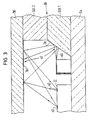
- the light emitted by the optical transmitter oS for example a laser diode, in the direction of the deflection element Ue is deflected by this deflection element Ue to a light distribution device Hol which is attached or formed on the underside of the cover body DK and which distributes the supplied light to optical detectors oD, which are integrated on a semiconductor chip with an integrated circuit IC, for example in the form of photo detectors.
- the light distribution device Hol can be a hologram, for example.
- the embodiment according to FIG. 3 has the advantage that it is compatible with the embodiments according to FIGS. 1 and 2.
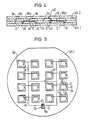
- FIGS. 4 and 5 show an embodiment in which both the optical connection according to FIGS. 1 and 2 and the optical connection according to FIG. 3 are realized on the same substrate Su.
- the substrate Su consists of a silicon wafer on which a first layer Sch1 of the spacer Ah is fixed, in which rectangular areas Be are recessed.
- a semiconductor chip with an integrated circuit IC and an optical transmitter oS is arranged in each rectangular area Be.
- There is also one on this layer Sch1 Strip waveguide structure Wst is formed, the waveguide of which transmits the light emitted by an optical transmitter oS of a clock generator TG to optical detectors oD of the various integrated circuits IC.
- FIG. 5 shows a top view of the layer Sch1 with the waveguide structure Wst.
- the side surfaces of the recessed areas Be of the first layer Sch1 are oblique so that they can form deflection elements Ue.
- a second layer Sch2 of the spacer Ah is applied to the waveguide structure Wst, which has recessed areas Be which coincide with the recessed areas Be of the first layer Sch1.
- the cover body DK is applied to the second layer Sch2.
- a light distribution element Hol is attached to the underside of the cover body DK, so that an optical connection according to FIG. 3 is implemented in each area.
- the recessed areas Be can be produced with high accuracy by etching or anisotropically etching silicon wafers. Since the same material is used for all layers, no thermal stresses occur.
- the substrate Su, the spacer Ah and the cover body DK can be fixed relative to one another, for example, by gluing them together or by screwing them together.
Landscapes
- Physics & Mathematics (AREA)
- Electromagnetism (AREA)
- Engineering & Computer Science (AREA)
- Computer Networks & Wireless Communication (AREA)
- Signal Processing (AREA)
- General Physics & Mathematics (AREA)
- Optics & Photonics (AREA)
- Optical Couplings Of Light Guides (AREA)
- Optical Communication System (AREA)
- Photo Coupler, Interrupter, Optical-To-Optical Conversion Devices (AREA)
- Optical Integrated Circuits (AREA)
Applications Claiming Priority (2)
| Application Number | Priority Date | Filing Date | Title |
|---|---|---|---|
| DE3811028 | 1988-03-31 | ||
| DE3811028 | 1988-03-31 |
Publications (2)
| Publication Number | Publication Date |
|---|---|
| EP0335104A2 true EP0335104A2 (fr) | 1989-10-04 |
| EP0335104A3 EP0335104A3 (fr) | 1991-11-06 |
Family
ID=6351182
Family Applications (1)
| Application Number | Title | Priority Date | Filing Date |
|---|---|---|---|
| EP19890103004 Withdrawn EP0335104A3 (fr) | 1988-03-31 | 1989-02-21 | Dispositif pour relier optiquement un ou plusieurs émetteurs optiques d'un ou plusieurs circuits intégrés |
Country Status (3)
| Country | Link |
|---|---|
| US (1) | US4871224A (fr) |
| EP (1) | EP0335104A3 (fr) |
| JP (1) | JPH0210876A (fr) |
Cited By (2)
| Publication number | Priority date | Publication date | Assignee | Title |
|---|---|---|---|---|
| EP0508613A1 (fr) * | 1991-04-08 | 1992-10-14 | Mitsubishi Denki Kabushiki Kaisha | Système à plusieurs puces électroniques et procédé pour alimenter celui-ci en signaux d'horloge |
| CN110727046A (zh) * | 2018-07-16 | 2020-01-24 | 上海新微技术研发中心有限公司 | 三维集成光互连芯片中光耦合端面的制造方法 |
Families Citing this family (70)
| Publication number | Priority date | Publication date | Assignee | Title |
|---|---|---|---|---|
| DE3834335A1 (de) * | 1988-10-08 | 1990-04-12 | Telefunken Systemtechnik | Halbleiterschaltung |
| GB8902745D0 (en) * | 1989-02-08 | 1989-03-30 | British Telecomm | Optical interconnection network |
| DE3910710A1 (de) * | 1989-04-03 | 1990-10-04 | Standard Elektrik Lorenz Ag | Optisch-elektrische mehrfachverbindung |
| JPH0642527B2 (ja) * | 1989-10-10 | 1994-06-01 | 日本電気株式会社 | 光導波路を用いた情報処理装置 |
| DE69009448T2 (de) * | 1990-03-08 | 1994-12-01 | Ibm | Halbleiterlaseranordnung. |
| US5163113A (en) * | 1990-07-19 | 1992-11-10 | Gte Laboratories Incorporated | Laser-to-fiber coupling apparatus |
| US5243671A (en) * | 1990-07-19 | 1993-09-07 | Gte Laboratories Incorporated | Laser-to-fiber coupling apparatus |
| GB9024713D0 (en) * | 1990-11-14 | 1991-01-02 | Plessey Telecomm | Optical backplane interconnecting circuit boards |
| US5121457A (en) * | 1991-05-21 | 1992-06-09 | Gte Laboratories Incorporated | Method for coupling laser array to optical fiber array |
| US5239189A (en) * | 1991-06-07 | 1993-08-24 | Eastman Kodak Company | Integrated light emitting and light detecting device |
| EP0522417A1 (fr) * | 1991-07-09 | 1993-01-13 | Sumitomo Electric Industries, Limited | Dispositif de réception de lumière avec connexion à fibre optique |
| US5200631A (en) * | 1991-08-06 | 1993-04-06 | International Business Machines Corporation | High speed optical interconnect |
| US5237434A (en) * | 1991-11-05 | 1993-08-17 | Mcnc | Microelectronic module having optical and electrical interconnects |
| US5268973A (en) * | 1992-01-21 | 1993-12-07 | The University Of Texas System | Wafer-scale optical bus |
| WO1993021663A1 (fr) * | 1992-04-08 | 1993-10-28 | Georgia Tech Research Corporation | Procede d'arrachement de materiaux en couche mince d'un substrat de croissance |
| DE59308072D1 (de) * | 1992-12-03 | 1998-03-05 | Siemens Ag | Bidirektionaler optischer Sende- und Empfangsmodul |
| JPH07131063A (ja) * | 1993-11-01 | 1995-05-19 | Nec Corp | マルチチップモジュール |
| US5416861A (en) * | 1994-04-29 | 1995-05-16 | University Of Cincinnati | Optical synchronous clock distribution network and high-speed signal distribution network |
| US5500910A (en) * | 1994-06-30 | 1996-03-19 | The Whitaker Corporation | Passively aligned holographic WDM |
| US5479540A (en) * | 1994-06-30 | 1995-12-26 | The Whitaker Corporation | Passively aligned bi-directional optoelectronic transceiver module assembly |
| US5886971A (en) * | 1996-09-27 | 1999-03-23 | Digital Optics Corporation | Optical head structures including support substrates adjacent transparent substrates and related methods |
| US5771218A (en) * | 1996-09-27 | 1998-06-23 | Digital Optics Corporation | Passively aligned integrated optical head including light source, detector, and optical element and methods of forming same |
| US5761350A (en) * | 1997-01-22 | 1998-06-02 | Koh; Seungug | Method and apparatus for providing a seamless electrical/optical multi-layer micro-opto-electro-mechanical system assembly |
| US6049639A (en) * | 1997-12-19 | 2000-04-11 | Intel Corporation | Method and apparatus providing optical input/output through the back side of an integrated circuit die |
| US6075908A (en) * | 1997-12-19 | 2000-06-13 | Intel Corporation | Method and apparatus for optically modulating light through the back side of an integrated circuit die |
| US6374003B1 (en) | 1997-12-19 | 2002-04-16 | Intel Corporation | Method and apparatus for optically modulating light through the back side of an integrated circuit die using a plurality of optical beams |
| US6330376B1 (en) | 1997-12-19 | 2001-12-11 | Intel Corporation | Higher order rejection method and apparatus for optical modulator |
| US6393169B1 (en) | 1997-12-19 | 2002-05-21 | Intel Corporation | Method and apparatus for providing optical interconnection |
| US6052498A (en) * | 1997-12-19 | 2000-04-18 | Intel Corporation | Method and apparatus providing an optical input/output bus through the back side of an integrated circuit die |
| US5978526A (en) * | 1997-12-19 | 1999-11-02 | Motorola, Inc. | Method, multi-channel optical interconnect device, and a multi-channel optically interconnected electronic device for minimizing cross-talk between a plurality of optical signals |
| JPH11311721A (ja) * | 1998-02-27 | 1999-11-09 | Oki Electric Ind Co Ltd | 光結合モジュールおよびその製造方法 |
| US6706546B2 (en) | 1998-10-09 | 2004-03-16 | Fujitsu Limited | Optical reflective structures and method for making |
| US6343171B1 (en) | 1998-10-09 | 2002-01-29 | Fujitsu Limited | Systems based on opto-electronic substrates with electrical and optical interconnections and methods for making |
| US6684007B2 (en) | 1998-10-09 | 2004-01-27 | Fujitsu Limited | Optical coupling structures and the fabrication processes |
| US6611635B1 (en) | 1998-10-09 | 2003-08-26 | Fujitsu Limited | Opto-electronic substrates with electrical and optical interconnections and methods for making |
| US6690845B1 (en) | 1998-10-09 | 2004-02-10 | Fujitsu Limited | Three-dimensional opto-electronic modules with electrical and optical interconnections and methods for making |
| US6845184B1 (en) | 1998-10-09 | 2005-01-18 | Fujitsu Limited | Multi-layer opto-electronic substrates with electrical and optical interconnections and methods for making |
| US6785447B2 (en) | 1998-10-09 | 2004-08-31 | Fujitsu Limited | Single and multilayer waveguides and fabrication process |
| US6587605B2 (en) | 1999-01-06 | 2003-07-01 | Intel Corporation | Method and apparatus for providing optical interconnection |
| US6901221B1 (en) | 1999-05-27 | 2005-05-31 | Jds Uniphase Corporation | Method and apparatus for improved optical elements for vertical PCB fiber optic modules |
| US6213651B1 (en) | 1999-05-26 | 2001-04-10 | E20 Communications, Inc. | Method and apparatus for vertical board construction of fiber optic transmitters, receivers and transceivers |
| US20040041081A1 (en) * | 2002-08-30 | 2004-03-04 | Feldman Michael R. | Integrated optical transceiver and related methods |
| US20070181781A1 (en) * | 2001-03-06 | 2007-08-09 | Digital Optics Corporation | Integrated optical transceiver |
| US6215577B1 (en) | 1999-10-25 | 2001-04-10 | Intel Corporation | Method and apparatus for optically modulating an optical beam with a multi-pass wave-guided optical modulator |
| US6501092B1 (en) | 1999-10-25 | 2002-12-31 | Intel Corporation | Integrated semiconductor superlattice optical modulator |
| US6268953B1 (en) | 1999-12-02 | 2001-07-31 | Intel Corporation | Method and apparatus for optically modulating an optical beam with long interaction length optical modulator |
| US6351326B1 (en) | 1999-12-14 | 2002-02-26 | Intel Corporation | Method and apparatus for optically modulating light utilizing a resonant cavity structure |
| JP2001274528A (ja) | 2000-01-21 | 2001-10-05 | Fujitsu Ltd | 薄膜デバイスの基板間転写方法 |
| US7842914B2 (en) * | 2000-03-06 | 2010-11-30 | Tessera North America, Inc. | Optoelectronic package, camera including the same and related methods |
| JP2003526909A (ja) * | 2000-03-06 | 2003-09-09 | ディジタル・オプティックス・コーポレイション | 集積化された光トランシーバおよび関連方法 |
| US6947615B2 (en) | 2001-05-17 | 2005-09-20 | Sioptical, Inc. | Optical lens apparatus and associated method |
| US6646747B2 (en) | 2001-05-17 | 2003-11-11 | Sioptical, Inc. | Interferometer apparatus and associated method |
| US6493502B1 (en) | 2001-05-17 | 2002-12-10 | Optronx, Inc. | Dynamic gain equalizer method and associated apparatus |
| US6891685B2 (en) * | 2001-05-17 | 2005-05-10 | Sioptical, Inc. | Anisotropic etching of optical components |
| US6608945B2 (en) | 2001-05-17 | 2003-08-19 | Optronx, Inc. | Self-aligning modulator method and associated apparatus |
| US6690844B2 (en) | 2001-05-17 | 2004-02-10 | Optronx, Inc. | Optical fiber apparatus and associated method |
| US6912330B2 (en) | 2001-05-17 | 2005-06-28 | Sioptical Inc. | Integrated optical/electronic circuits and associated methods of simultaneous generation thereof |
| US6654511B2 (en) | 2001-05-17 | 2003-11-25 | Sioptical, Inc. | Optical modulator apparatus and associated method |
| US6603889B2 (en) | 2001-05-17 | 2003-08-05 | Optronx, Inc. | Optical deflector apparatus and associated method |
| US6748125B2 (en) | 2001-05-17 | 2004-06-08 | Sioptical, Inc. | Electronic semiconductor control of light in optical waveguide |
| US6625348B2 (en) | 2001-05-17 | 2003-09-23 | Optron X, Inc. | Programmable delay generator apparatus and associated method |
| US6526187B1 (en) | 2001-05-17 | 2003-02-25 | Optronx, Inc. | Polarization control apparatus and associated method |
| US6529318B1 (en) | 2001-08-30 | 2003-03-04 | Np Photonics, Inc. | Total internal reflection (TIR) coupler and method for side-coupling pump light into a fiber |
| EP1335507B1 (fr) * | 2002-01-31 | 2005-09-14 | STMicroelectronics S.r.l. | Methode et dispositif pour une excellente isolation galvanique entre deux circuits basse tension dans un isolateur optique |
| US7110629B2 (en) * | 2002-07-22 | 2006-09-19 | Applied Materials, Inc. | Optical ready substrates |
| US7043106B2 (en) * | 2002-07-22 | 2006-05-09 | Applied Materials, Inc. | Optical ready wafers |
| US20050016446A1 (en) | 2003-07-23 | 2005-01-27 | Abbott John S. | CaF2 lenses with reduced birefringence |
| CN106842440A (zh) * | 2012-03-05 | 2017-06-13 | 纳米精密产品股份有限公司 | 用于耦合光纤输入/输出的具有结构化反射表面的耦合装置 |
| US9880366B2 (en) | 2015-10-23 | 2018-01-30 | Nanoprecision Products, Inc. | Hermetic optical subassembly |
| US10705302B2 (en) * | 2018-02-27 | 2020-07-07 | Samsung Electronics Co., Ltd. | Photonic integrated circuit packages |
Family Cites Families (6)
| Publication number | Priority date | Publication date | Assignee | Title |
|---|---|---|---|---|
| DE2510562C2 (de) * | 1975-03-11 | 1985-04-18 | Siemens AG, 1000 Berlin und 8000 München | Optoelektronisches Koppelelement |
| US4136928A (en) * | 1977-05-06 | 1979-01-30 | Bell Telephone Laboratories, Incorporated | Optical integrated circuit including junction laser with oblique mirror |
| US4675518A (en) * | 1982-03-05 | 1987-06-23 | Omron Tateisi Electronics Co. | Optical bistable device |
| JPS60121347U (ja) * | 1984-01-24 | 1985-08-16 | ソニー株式会社 | 光送受信装置 |
| US4699449A (en) * | 1985-03-05 | 1987-10-13 | Canadian Patents And Development Limited-Societe Canadienne Des Brevets Et D'exploitation Limitee | Optoelectronic assembly and method of making the same |
| EP0253886A1 (fr) * | 1986-01-21 | 1988-01-27 | AT&T Corp. | Interconnexion pour un ensemble integre a l'echelle d'une tranche |
-
1989
- 1989-02-21 EP EP19890103004 patent/EP0335104A3/fr not_active Withdrawn
- 1989-03-13 US US07/322,410 patent/US4871224A/en not_active Expired - Fee Related
- 1989-03-29 JP JP1080204A patent/JPH0210876A/ja active Pending
Cited By (4)
| Publication number | Priority date | Publication date | Assignee | Title |
|---|---|---|---|---|
| EP0508613A1 (fr) * | 1991-04-08 | 1992-10-14 | Mitsubishi Denki Kabushiki Kaisha | Système à plusieurs puces électroniques et procédé pour alimenter celui-ci en signaux d'horloge |
| US5250816A (en) * | 1991-04-08 | 1993-10-05 | Mitsubishi Denki Kabushiki Kaisha | Multichip system and method of supplying clock signal therefor |
| CN110727046A (zh) * | 2018-07-16 | 2020-01-24 | 上海新微技术研发中心有限公司 | 三维集成光互连芯片中光耦合端面的制造方法 |
| CN110727046B (zh) * | 2018-07-16 | 2021-07-23 | 上海新微技术研发中心有限公司 | 三维集成光互连芯片中光耦合端面的制造方法 |
Also Published As
| Publication number | Publication date |
|---|---|
| JPH0210876A (ja) | 1990-01-16 |
| EP0335104A3 (fr) | 1991-11-06 |
| US4871224A (en) | 1989-10-03 |
Similar Documents
| Publication | Publication Date | Title |
|---|---|---|
| EP0335104A2 (fr) | Dispositif pour relier optiquement un ou plusieurs émetteurs optiques d'un ou plusieurs circuits intégrés | |
| DE3880234T2 (de) | Ausrichten von glasfaser-arrays. | |
| EP0366974B1 (fr) | Circuit semi-conducteur | |
| DE3885213T2 (de) | Mittel, um eine optische Fiber an ein opto-elektronisches Bauelement anzukoppeln. | |
| DE68929065T2 (de) | Unterbaugruppe für optoelektronische Bauelemente | |
| DE69525701T2 (de) | Integrierter optoelektronischer Verbund und Stecker | |
| DE3687063T2 (de) | Optische komponente mit wellenleiter. | |
| DE3390103C2 (fr) | ||
| DE69132202T2 (de) | Methode zum passiven Ausrichten von Diodenlaser-Arrays und optischen Fasern | |
| DE69110961T2 (de) | Optischer Schaltkreis für Oberflächenmontage, Substrat dafür und seine Herstellungsmethode. | |
| DE69618035T2 (de) | Vorrichtung zur ausrichtung eines optoelektronischen bauteils | |
| DE69010138T2 (de) | Anordnung zur Ausrichtung optischer Fasern und Herstellungsmethode dafür. | |
| DE60303140T2 (de) | Optische verbindungsanordnung | |
| DE3138296C2 (fr) | ||
| DE60215019T2 (de) | Trennung von integrierten optischen modulen und strukturen | |
| DE19621124A1 (de) | Optoelektronischer Wandler und dessen Herstellungsverfahren | |
| DE19830360A1 (de) | Opto-elektronischer Modul | |
| DE19727483A1 (de) | Röntgenstrahl-CT-Festkörperdetektor | |
| DE69833611T2 (de) | Ein Mikro-Photonikmodul mit einer Trennwand | |
| DE68929527T2 (de) | Optische Übertragungsvorrichtung | |
| EP0463297A1 (fr) | Dispositif comprenant un substrat et un composant et procédé de fabrication | |
| EP1168022A2 (fr) | Module opto-électronique avec substat à connexions traversantes | |
| DE69015588T2 (de) | Optischer Kopf integrierbar in einem hybriden Schaltkreis. | |
| DE2734798C2 (fr) | ||
| DE102019210750B4 (de) | Verfahren zur herstellung einer anordnung mit einem substrat und zwei bauelementen mit lichtwellenleitern |
Legal Events
| Date | Code | Title | Description |
|---|---|---|---|
| PUAI | Public reference made under article 153(3) epc to a published international application that has entered the european phase |
Free format text: ORIGINAL CODE: 0009012 |
|
| AK | Designated contracting states |
Kind code of ref document: A2 Designated state(s): DE FR GB |
|
| 17P | Request for examination filed |
Effective date: 19901205 |
|
| PUAL | Search report despatched |
Free format text: ORIGINAL CODE: 0009013 |
|
| AK | Designated contracting states |
Kind code of ref document: A3 Designated state(s): DE FR GB |
|
| 17Q | First examination report despatched |
Effective date: 19940510 |
|
| STAA | Information on the status of an ep patent application or granted ep patent |
Free format text: STATUS: THE APPLICATION IS DEEMED TO BE WITHDRAWN |
|
| 18D | Application deemed to be withdrawn |
Effective date: 19950505 |