EP0508627A2 - Verfahren und Anordnung zur Erzeugung von Übertragsignalen - Google Patents
Verfahren und Anordnung zur Erzeugung von Übertragsignalen Download PDFInfo
- Publication number
- EP0508627A2 EP0508627A2 EP92302413A EP92302413A EP0508627A2 EP 0508627 A2 EP0508627 A2 EP 0508627A2 EP 92302413 A EP92302413 A EP 92302413A EP 92302413 A EP92302413 A EP 92302413A EP 0508627 A2 EP0508627 A2 EP 0508627A2
- Authority
- EP
- European Patent Office
- Prior art keywords
- carry out
- carry
- value
- values
- determining
- Prior art date
- Legal status (The legal status is an assumption and is not a legal conclusion. Google has not performed a legal analysis and makes no representation as to the accuracy of the status listed.)
- Granted
Links
Images






Classifications
-
- G—PHYSICS
- G06—COMPUTING OR CALCULATING; COUNTING
- G06F—ELECTRIC DIGITAL DATA PROCESSING
- G06F7/00—Methods or arrangements for processing data by operating upon the order or content of the data handled
- G06F7/38—Methods or arrangements for performing computations using exclusively denominational number representation, e.g. using binary, ternary, decimal representation
- G06F7/48—Methods or arrangements for performing computations using exclusively denominational number representation, e.g. using binary, ternary, decimal representation using non-contact-making devices, e.g. tube, solid state device; using unspecified devices
- G06F7/50—Adding; Subtracting
- G06F7/505—Adding; Subtracting in bit-parallel fashion, i.e. having a different digit-handling circuit for each denomination
- G06F7/506—Adding; Subtracting in bit-parallel fashion, i.e. having a different digit-handling circuit for each denomination with simultaneous carry generation for, or propagation over, two or more stages
- G06F7/507—Adding; Subtracting in bit-parallel fashion, i.e. having a different digit-handling circuit for each denomination with simultaneous carry generation for, or propagation over, two or more stages using selection between two conditionally calculated carry or sum values
-
- G—PHYSICS
- G06—COMPUTING OR CALCULATING; COUNTING
- G06F—ELECTRIC DIGITAL DATA PROCESSING
- G06F7/00—Methods or arrangements for processing data by operating upon the order or content of the data handled
- G06F7/38—Methods or arrangements for performing computations using exclusively denominational number representation, e.g. using binary, ternary, decimal representation
- G06F7/48—Methods or arrangements for performing computations using exclusively denominational number representation, e.g. using binary, ternary, decimal representation using non-contact-making devices, e.g. tube, solid state device; using unspecified devices
- G06F7/50—Adding; Subtracting
-
- G—PHYSICS
- G06—COMPUTING OR CALCULATING; COUNTING
- G06F—ELECTRIC DIGITAL DATA PROCESSING
- G06F7/00—Methods or arrangements for processing data by operating upon the order or content of the data handled
- G06F7/38—Methods or arrangements for performing computations using exclusively denominational number representation, e.g. using binary, ternary, decimal representation
- G06F7/48—Methods or arrangements for performing computations using exclusively denominational number representation, e.g. using binary, ternary, decimal representation using non-contact-making devices, e.g. tube, solid state device; using unspecified devices
- G06F7/544—Methods or arrangements for performing computations using exclusively denominational number representation, e.g. using binary, ternary, decimal representation using non-contact-making devices, e.g. tube, solid state device; using unspecified devices for evaluating functions by calculation
Definitions
- This invention relates to computer circuits and, more particularly, to methods and apparatus for rapidly generating the carry out signals for adder circuits.
- Adder circuits are used in digital computers for many purposes. In most of those uses, the speed of those circuits is paramount. For example, the primary manner in which the sequential flow of information is changed in a digital computer is through the use of conditional branch operations.
- a conditional branch operation depends on some arithmetic operation and, based on the result, makes a decision whether or not to branch to a particular address.
- the result of the arithmetic operation usually involves a summation, carry outs, and a sign; and the decision may depends on any of these elements, combinations of these elements, or flags generated from these elements.
- the length of time required to generate flags which depend on the final carry out value is usually the critical element and is, consequently, a major factor in achieving higher processor speed.
- Carry look ahead, carry select, and Manchester carry chain schemes are some of the fast hardware implementations of adders.
- Carry look ahead adders and Manchester carry chain adders are limited in speed because their operation is inherently serial in nature.
- Carry select adders compute two results of groups of digits in parallel and select the correct one of the two after the carry-in value to the group is known. When a number of columns are computed in parallel as subsets, at least in theory very fast operation could result. However, in reality such adders take up a great deal of circuitry and are therefore expensive to implement and slower than theoretically predicted. An arrangement is needed which operates rapidly yet does not utilize the very large amount of circuitry required by the prior art.
- an object of the present invention to provide new circuitry for computing the carry out from the summation of two binary numbers. It is another more specific object of the present invention to provide circuitry which computes the carry out of the sum of two binary numbers rapidly and separately from the sum of the two numbers.
- Figure 1 is a block diagram of a typical adder circuit of the prior art.
- Figure 2 is a block diagram of a conditional sum adder proposed by the prior art.
- Figure 3 is a block diagram of a first carry compute circuit constructed in accordance with the invention.
- Figure 4 is a block diagram of a second carry compute circuit constructed in accordance with the invention.
- Figure 5 is a circuit diagram of a portion of the circuit illustrated in Figure 4.
- Figure 6 is a circuit diagram of another portion of the circuit illustrated in Figure 4.
- Figure 7 is a block diagram of a third carry compute circuit constructed in accordance with the invention.
- FIGS 8-11 are circuit diagrams of portions of the circuit illustrated in Figure 7.
- the manipulations performed are often referred to in terms, such as adding or comparing, which are commonly associated with mental operations performed by a human operator. No such capability of a human operator is necessary or desirable in most cases in any of the operations described herein which form part of the present invention; the operations are machine operations. In all cases the distinction between the method operations in operating a machine and the method of computation itself should be borne in mind.
- the present invention relates to apparatus and to method steps for operating a computer in processing electrical or other (e.g. mechanical, chemical) physical signals to generate other desired physical signals.
- Figure 1 illustrates a typical arrangement for obtaining the rapid addition of two binary numbers.
- a first carry-look-ahead adder 12 is utilized to add together the lower four bits of two binary numbers A and B.
- the adder 12 receives the carry-in signal Cin0 and propagates that signal through the stages combining it with the bits being added at the various stages to produce a result S0-S3 and a carry-out signal C3 from the last stage.
- an adder circuit 14 receives the higher order bits 4-7 of the two binary numbers A and B and computes a sum S1_4-S1_7 and a carry out C1_7 presuming a carry in from stage three of one; and an adder circuit 16 is furnished the higher order bits of the two numbers A and B and computes a sum S0_4-S0_7 and a carry out C0_7 presuming a carry in from stage three of Zero.
- the correct higher order sum bits are selected by the final carry out C3 from the adder 12 using a multiplexor 18.
- the correct final carry out "not C8" is produced by an OR gate 20 and an NAND gate 22 which select from the two possibilities depending on the condition of the carry out C3.
- Figure 2 illustrates a conditional carry adder proposed by Sklansky in the above-mentioned paper.
- this adder two seven bit numbers are added bit by bit (represented by x0y0 through x6y6) at a first level by bit adders H to produce four possible outputs from each of the adder circuits: a sum produced if the carry in is zero, a sum produced if the carry in is one, a carry out produced if the carry in is zero, and a carry out produced if the carry in is one.
- the output signals produced by alternate ones of these first level adder circuits H are furnished to pairs of second level circuits Q1.
- the circuits Q1 are enabled by either a carry in zero or a carry in one from the output of the preceeding bit.
- FIG. 3 illustrates a block diagram of a basic circuit constructed in accordance with the invention.
- the circuit 30 illustrated in Figure 3 is utilized to generate the carry-out bit from the addition of two eight bit binary numbers. Only the lower seven bits of an eight bit number need be used to obtain the carry out value and the other values necessary to the determination of conditional branch equations as will be seen from the discussion which follows.
- the circuit 30 includes seven individual carry generator circuits 32 which are individually designated carry generator 0 through carry generator 6. Each carry generator circuit 32 receives as input two bits, one each from the addend and the augend, at the particular bit position. Thus, the two lowest order bits to be summed are placed in the carry generator 0. Simultaneously, all of the other carry generators 1-6 receives the two bits of the augend and addend at their particular bit positions.
- Each carry generator 32 produces two possible carry out values; these values are the carry out from the stage if the carry in to that bit is a zero and the carry out from the stage if the carry in is a one.
- these signals are designated C0-0-1 and CO-1-1, the designation indicating first a carry out for bit 0, next a carry out for a zero or one carry in value, and finally that the carry outs result from a single level of determination.
- the carry out signals from the other carry generators 32 and the other circuitry described are similarly designated.
- the results produced by the carry generators 32 may be summarized by the two equations placed under the title "Carry Generator” to the right of the circuitry in Figure 3. That is, the carry out signal where the carry in signal is a zero (Cout_0) can be a one only if both of the bits summed at that level are ones. Additionally, the carry out signal where the carry in signal is a one (Cout_1) can be a one only if one of the bits summed at that level is a one. These two carry out signals are propagated from each of the carry generators 32 to the next stage.
- the carry out values from each of the carry generators 0-6 are transferred to a second stage. For the lowest order bit 0, this stage is a carry selector 34.
- the carry selector 34 receives the two possible carry out values from the preceding stage (carry generator 0 in this case) and selects the correct one of the two based on the actual carry in value Cprev from the preceding stage.
- This carry select operation may be expressed by the equations for "Carry Select" shown to the right in the drawing in Figure 3. It may be seen that the carry out for a zero carry in is selected if the carry in Cprev from the previous stage is zero, and the carry out for a one carry in is selected if the carry in Cprev from the previous stage is one.
- the carry selector 0 thus produces the actual carry out C0 from the bit 0 stage at the first level. This result is transferred to an identical carry selector circuit 34 identified as carry selector 2. The carry out C2 from carry selector 2 is in turn transferred to an identical carry selector 6.
- each bit stage other than bit 0 the two possible carry outs from the carry generator circuit 32 are furnished to a carry expander circuit 36.
- Four of these carry expander circuits 36 are illustrated in Figure 3, and each operates in the same manner.
- Each expander circuit 36 on the first level (expanders 2, 4, and 6) receives from the carry generators 32 of two adjacent bit positions the two possible carry outs from those bit positions, and provides two possible carry out signals based on those four possible inputs.
- the carry expander 2 receives the carry out signals C1-0-1 and C1-1-1 from the carry generator 1 for bit 1, and the carry out signals C2-0-1 and C2-1-1 from the carry generator 2 for bit 2.
- each carry expander circuit 36 The two possible values produced by each carry expander circuit 36 are transferred to either a carry selector circuit 34 or another carry expander 36 depending on the level of the bits involved. At the bit two level, the two carry outs are transferred to a carry selector 2, for example, where the carry out C0 from carry selector 0 selects the appropriate one of the two carry out signals which result from the four possible carry outs at the carry generator level.
- the two carry outs from carry expander 4 and the two carry outs from carry expander 6, on the other hand, are both transferred as the inputs to a second level carry expander 6-2.
- the carry out function is separated from the summing function in the invention, the intermediate carry out bits are used only to generate higher order carry out bits and are not delayed by the necessity to be utilized in generating a plurality of summations as in the circuit illustrated in Figures 1 and 2. In fact, the separation of carry from adder makes "the maximum fanout a constant rather than an increasing function of the summand length.”
- the carry out bit C6 may be utilized in an eight bit adder since it is only necessary that the next to most significant bit be available to compute the carry out from the most significant bit.
- Figure 3 four stages of operation are required for computing the carry out in adding two eight bit binary numbers using the circuit described therein.
- a further improvement in speed may be attained by recognizing that the carry expander and carry selector circuits do not have to handle only two bits at a time. In fact, they may handle any number of bits and may be combined.
- Figure 4, for example illustrates a modified circuit 40 which produces the carry out signal from the addition of two eight bit numbers using only three stages of operation.
- the circuit 40 includes the same number of carry generator circuits 42 as does the circuit 20 of Figure 3.
- the circuit 40 includes only two carry expanders 44, a carry selector 46, and a second carry selector 48 to accomplish the production of the final carry out in only three levels and help to speed the production of the final carry out signal.
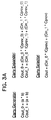
- the carry expanders 44 each receive a pair of possible carry out signals from each of three (rather than two) individual carry generators 42 and produce a pair of possible carry out signals. These signals are generated in accordance with the equations illustrated in Figure 4.
- the carry selector 46 is identical to the carry selectors 34 used in the circuit 30 of Figure 3 and produces a single carry out signal C0 resulting from the addition of the bits at bit 0 and the carry in signal.
- Carry selector 48 receives the two possible carry out signals from each of the carry expanders 46 and selects the appropriate carry out signal C6 based on the carry out C0 from the carry selector 46.
- the operation of the carry selector 48 is actually both carry expansion and selection and is based on the equations for that function illustrated in Figure 4.
- Figure 5 illustrates a circuit 50 which may be utilized to accomplish the functions described by the equations for the three bit carry expander circuit 44 illustrated in Figure 4.
- the circuit 50 receives the two possible carry out signals from each of three bit positions as inputs signals and produces a pair of possible output signals Cout_0 and Cout_1.
- the actual circuit is constructed of a plurality of p-channel FET devices (all of the devices above the Cprev_0 input line in the figure) and a plurality of n-channel FET devices (below the Cprev_0 input line in the figure).
- the p-channel devices are each turned on by zero signals applied to the gate terminal while the n-channel devices are each turned on by one signals applied to the gate terminal. This circuit construction applies for all of the circuit diagrams illustrated.
- the carry out signal Cout_0_ is not a one (is a zero, used because the circuit is carried out in inverting logic) under a number of different circumstances.
- One of these circumstances is if the carry out signal for a zero carry in of the highest of the three bits Cin2_0 is a one and the carry out signal for a zero carry in of the next highest of the three bits Cin1_0 is a zero and the carry out signal for a zero carry in of the next lowest of the three bits Cprev_0 is a zero.
- the connections made in the circuit in response to these three inputs can be seen to place ground at the Cout_0_terminal through the transistor A.
- the response of the circuit of Figure 5 may be seen to follow the other elements of the equations in a similar manner.
- circuit 50 provides faster operation than does the complete implementation of these general equations.
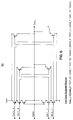
- FIG. 6 illustrates in a similar manner a circuit 60 which may be utilized to accomplish the functions described by the equations for the carry selector circuit 48 illustrated in Figure 4.
- the operation of the selector may be understood from considering the equations for that three bit selector in Figure 4. For example, the carry out signal Cout_ is not a one (is a zero) under a number of different circumstances.
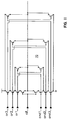
- a circuit designed in accordance with the present invention for producing the carry out signal for a thirty-two bit addition is illustrated in Figure 7.
- the elements of the block diagram include two bit carry generation and expander circuits 64 which serve the functions of both generating and expanding from a pair of bit positions, three four bit carry expander circuits 66, one two bit carry generation and selector circuit 68 which serves the functions of both generating and selecting from a single bit position, and two four bit carry selectors 70.
- the circuits 64 function in the manner described above to generate the possible carry outs at each of a pair of bit positions 1-30 and combine each the carry outs from each two adjacent bits after the first bit to produce two more possible carry outs.
- the circuits 66 further combine the results of each four combination for bits 7-30 to reach two more possible carry outs.
- the possible carry outs from the circuits 66 are all provided as inputs to the rightmost selector circuit 70.
- the possible carry outs from the circuits 64 from bits 1-6 are furnished to the leftmost carry selector circuit 70 and the carry out C6 is selected using the carry out C0 determined for bit 0 by the carry generator and selector circuit 68.
- the carry out C6 from the carry selector circuit 70 which selects from the first seven bit levels is used to select the carry out C30 from the rightmost circuit 70 which is used to generate the flags necessary to control the conditional operations mentioned above.
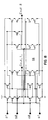
- a two bit carry generator and expansion circuit 64 is illustrated in Figure 8.
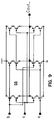
- a two bit carry generator and selector circuit 68 is illustrated in Figure 9.
- a four bit carry expander circuit 66 is illustrated in Figure 10.
- a four bit selector circuit 70 is illustrated in Figure 11.
- Each of these circuits is designed in a similar manner to the circuits discussed in detail above to provide the fastest possible carry out response by eliminating redundant transistors. It should be noted that the merger of the carry out generation and expansion in the circuit 64 and the carry generation and selection in the circuit 68 help reduce the number of stages of the circuit of Figure 7 by one and thus reduce the time required to generate the ultimate carry out signal.
Landscapes
- Engineering & Computer Science (AREA)
- Physics & Mathematics (AREA)
- General Physics & Mathematics (AREA)
- Theoretical Computer Science (AREA)
- Pure & Applied Mathematics (AREA)
- Computational Mathematics (AREA)
- Mathematical Analysis (AREA)
- Computing Systems (AREA)
- General Engineering & Computer Science (AREA)
- Mathematical Optimization (AREA)
- Logic Circuits (AREA)
- Compression, Expansion, Code Conversion, And Decoders (AREA)
- Complex Calculations (AREA)
Applications Claiming Priority (2)
| Application Number | Priority Date | Filing Date | Title |
|---|---|---|---|
| US68257591A | 1991-04-08 | 1991-04-08 | |
| US682575 | 1991-04-08 |
Publications (3)
| Publication Number | Publication Date |
|---|---|
| EP0508627A2 true EP0508627A2 (de) | 1992-10-14 |
| EP0508627A3 EP0508627A3 (en) | 1994-07-13 |
| EP0508627B1 EP0508627B1 (de) | 1999-01-13 |
Family
ID=24740277
Family Applications (1)
| Application Number | Title | Priority Date | Filing Date |
|---|---|---|---|
| EP92302413A Expired - Lifetime EP0508627B1 (de) | 1991-04-08 | 1992-03-20 | Verfahren und Anordnung zur Erzeugung von Übertragsignalen |
Country Status (4)
| Country | Link |
|---|---|
| EP (1) | EP0508627B1 (de) |
| JP (1) | JP3286793B2 (de) |
| KR (1) | KR100256103B1 (de) |
| DE (1) | DE69228140T2 (de) |
Cited By (1)
| Publication number | Priority date | Publication date | Assignee | Title |
|---|---|---|---|---|
| GB2263002B (en) * | 1992-01-06 | 1995-08-30 | Intel Corp | A parallel binary adder |
Families Citing this family (1)
| Publication number | Priority date | Publication date | Assignee | Title |
|---|---|---|---|---|
| JP6454542B2 (ja) | 2014-12-26 | 2019-01-16 | Fdk株式会社 | 外付けptc素子、および筒形電池 |
Family Cites Families (3)
| Publication number | Priority date | Publication date | Assignee | Title |
|---|---|---|---|---|
| DE3346241A1 (de) * | 1983-03-31 | 1984-10-04 | Siemens AG, 1000 Berlin und 8000 München | Parallelverknuepfungsschaltung mit verkuerztem uebertragsdurchlauf |
| JPS60142423A (ja) * | 1983-12-28 | 1985-07-27 | Fujitsu Ltd | 条件コ−ド生成方式 |
| JPH01244531A (ja) * | 1988-03-25 | 1989-09-28 | Fujitsu Ltd | 論理回路 |
-
1992
- 1992-03-20 EP EP92302413A patent/EP0508627B1/de not_active Expired - Lifetime
- 1992-03-20 DE DE69228140T patent/DE69228140T2/de not_active Expired - Fee Related
- 1992-04-01 KR KR1019920005429A patent/KR100256103B1/ko not_active Expired - Fee Related
- 1992-04-08 JP JP11430192A patent/JP3286793B2/ja not_active Expired - Fee Related
Cited By (1)
| Publication number | Priority date | Publication date | Assignee | Title |
|---|---|---|---|---|
| GB2263002B (en) * | 1992-01-06 | 1995-08-30 | Intel Corp | A parallel binary adder |
Also Published As
| Publication number | Publication date |
|---|---|
| KR920020313A (ko) | 1992-11-21 |
| JPH0628157A (ja) | 1994-02-04 |
| JP3286793B2 (ja) | 2002-05-27 |
| KR100256103B1 (ko) | 2000-05-01 |
| DE69228140T2 (de) | 1999-08-19 |
| DE69228140D1 (de) | 1999-02-25 |
| EP0508627A3 (en) | 1994-07-13 |
| EP0508627B1 (de) | 1999-01-13 |
Similar Documents
| Publication | Publication Date | Title |
|---|---|---|
| JP3729881B2 (ja) | 並列加算および平均演算を行うための回路およびその方法 | |
| US3993891A (en) | High speed parallel digital adder employing conditional and look-ahead approaches | |
| JP3578502B2 (ja) | 単一プロセッサにおいて並列データ処理を実行する方法 | |
| EP0585619B1 (de) | Verfahren zur Feststellung eines nullwertigen Ergebnisses als Folge einer arithmetischen oder logischen Berechnung und Schaltung hierfür | |
| US6411980B2 (en) | Data split parallel shifter and parallel adder/subtractor | |
| US4525797A (en) | N-bit carry select adder circuit having only one full adder per bit | |
| JPH07210368A (ja) | 算術演算の結果として生じる正および負のオーバーフローのハードウェアによる効率的な取り扱い方法 | |
| JPH07200261A (ja) | 論理演算装置 | |
| US6018757A (en) | Zero detect for binary difference | |
| US5367477A (en) | Method and apparatus for performing parallel zero detection in a data processing system | |
| US5375078A (en) | Arithmetic unit for performing XY+B operation | |
| JPH01112332A (ja) | 乗算及び算術論理演算機能を組合わせて使用する浮動小数点ユニット | |
| JPH0823811B2 (ja) | 3オペランド演算論理機構におけるオーバーフローを決定する方法及び算術上のオーバーフローを検出する機構 | |
| US5235539A (en) | Method and apparatus for generating carry out signals | |
| US4764888A (en) | N-bit carry select adder circuit with double carry select generation | |
| US6362645B2 (en) | Logic circuits and carry-lookahead circuits | |
| JP3225043B2 (ja) | 絶対値算術演算ユニット及び差動マルチプレクサ | |
| US5867413A (en) | Fast method of floating-point multiplication and accumulation | |
| EP0670061B1 (de) | Verbesserter schneller multiplizierer | |
| Issa et al. | High precision binary coded decimal (bcd) unit for 128-bit addition | |
| EP0508627B1 (de) | Verfahren und Anordnung zur Erzeugung von Übertragsignalen | |
| US5920493A (en) | Apparatus and method to determine a most significant bit | |
| US5798958A (en) | Zero detect for binary sum | |
| US6826588B2 (en) | Method and apparatus for a fast comparison in redundant form arithmetic | |
| US7206802B2 (en) | Hybrid carry look ahead/carry select adder including carry logic generating complementary hot carry signals, and method for producing the carry logic |
Legal Events
| Date | Code | Title | Description |
|---|---|---|---|
| PUAI | Public reference made under article 153(3) epc to a published international application that has entered the european phase |
Free format text: ORIGINAL CODE: 0009012 |
|
| AK | Designated contracting states |
Kind code of ref document: A2 Designated state(s): DE FR GB IT SE |
|
| PUAL | Search report despatched |
Free format text: ORIGINAL CODE: 0009013 |
|
| AK | Designated contracting states |
Kind code of ref document: A3 Designated state(s): DE FR GB IT SE |
|
| 17P | Request for examination filed |
Effective date: 19940929 |
|
| 17Q | First examination report despatched |
Effective date: 19970605 |
|
| GRAG | Despatch of communication of intention to grant |
Free format text: ORIGINAL CODE: EPIDOS AGRA |
|
| GRAG | Despatch of communication of intention to grant |
Free format text: ORIGINAL CODE: EPIDOS AGRA |
|
| GRAH | Despatch of communication of intention to grant a patent |
Free format text: ORIGINAL CODE: EPIDOS IGRA |
|
| GRAH | Despatch of communication of intention to grant a patent |
Free format text: ORIGINAL CODE: EPIDOS IGRA |
|
| GRAA | (expected) grant |
Free format text: ORIGINAL CODE: 0009210 |
|
| AK | Designated contracting states |
Kind code of ref document: B1 Designated state(s): DE FR GB IT SE |
|
| REF | Corresponds to: |
Ref document number: 69228140 Country of ref document: DE Date of ref document: 19990225 |
|
| ITF | It: translation for a ep patent filed | ||
| ET | Fr: translation filed | ||
| PLBE | No opposition filed within time limit |
Free format text: ORIGINAL CODE: 0009261 |
|
| STAA | Information on the status of an ep patent application or granted ep patent |
Free format text: STATUS: NO OPPOSITION FILED WITHIN TIME LIMIT |
|
| 26N | No opposition filed | ||
| REG | Reference to a national code |
Ref country code: GB Ref legal event code: IF02 |
|
| PGFP | Annual fee paid to national office [announced via postgrant information from national office to epo] |
Ref country code: SE Payment date: 20020305 Year of fee payment: 11 |
|
| PG25 | Lapsed in a contracting state [announced via postgrant information from national office to epo] |
Ref country code: SE Free format text: LAPSE BECAUSE OF NON-PAYMENT OF DUE FEES Effective date: 20030321 |
|
| PGFP | Annual fee paid to national office [announced via postgrant information from national office to epo] |
Ref country code: DE Payment date: 20030327 Year of fee payment: 12 |
|
| EUG | Se: european patent has lapsed | ||
| PGFP | Annual fee paid to national office [announced via postgrant information from national office to epo] |
Ref country code: FR Payment date: 20040309 Year of fee payment: 13 |
|
| PG25 | Lapsed in a contracting state [announced via postgrant information from national office to epo] |
Ref country code: DE Free format text: LAPSE BECAUSE OF NON-PAYMENT OF DUE FEES Effective date: 20041001 |
|
| PG25 | Lapsed in a contracting state [announced via postgrant information from national office to epo] |
Ref country code: IT Free format text: LAPSE BECAUSE OF NON-PAYMENT OF DUE FEES Effective date: 20050320 |
|
| PG25 | Lapsed in a contracting state [announced via postgrant information from national office to epo] |
Ref country code: FR Free format text: LAPSE BECAUSE OF NON-PAYMENT OF DUE FEES Effective date: 20051130 |
|
| REG | Reference to a national code |
Ref country code: FR Ref legal event code: ST Effective date: 20051130 |
|
| PGFP | Annual fee paid to national office [announced via postgrant information from national office to epo] |
Ref country code: GB Payment date: 20110316 Year of fee payment: 20 |
|
| REG | Reference to a national code |
Ref country code: GB Ref legal event code: PE20 Expiry date: 20120319 |
|
| PG25 | Lapsed in a contracting state [announced via postgrant information from national office to epo] |
Ref country code: GB Free format text: LAPSE BECAUSE OF EXPIRATION OF PROTECTION Effective date: 20120319 |