EP0508821A2 - Verfahren zur Herstellung von keramischen Mehrschichtsubstraten - Google Patents
Verfahren zur Herstellung von keramischen Mehrschichtsubstraten Download PDFInfo
- Publication number
- EP0508821A2 EP0508821A2 EP92303245A EP92303245A EP0508821A2 EP 0508821 A2 EP0508821 A2 EP 0508821A2 EP 92303245 A EP92303245 A EP 92303245A EP 92303245 A EP92303245 A EP 92303245A EP 0508821 A2 EP0508821 A2 EP 0508821A2
- Authority
- EP
- European Patent Office
- Prior art keywords
- glass
- green sheets
- glass powder
- layer
- powder
- Prior art date
- Legal status (The legal status is an assumption and is not a legal conclusion. Google has not performed a legal analysis and makes no representation as to the accuracy of the status listed.)
- Withdrawn
Links
Images




Classifications
-
- C—CHEMISTRY; METALLURGY
- C04—CEMENTS; CONCRETE; ARTIFICIAL STONE; CERAMICS; REFRACTORIES
- C04B—LIME, MAGNESIA; SLAG; CEMENTS; COMPOSITIONS THEREOF, e.g. MORTARS, CONCRETE OR LIKE BUILDING MATERIALS; ARTIFICIAL STONE; CERAMICS; REFRACTORIES; TREATMENT OF NATURAL STONE
- C04B38/00—Porous mortars, concrete, artificial stone or ceramic ware; Preparation thereof
-
- H—ELECTRICITY
- H10—SEMICONDUCTOR DEVICES; ELECTRIC SOLID-STATE DEVICES NOT OTHERWISE PROVIDED FOR
- H10W—GENERIC PACKAGES, INTERCONNECTIONS, CONNECTORS OR OTHER CONSTRUCTIONAL DETAILS OF DEVICES COVERED BY CLASS H10
- H10W70/00—Package substrates; Interposers; Redistribution layers [RDL]
- H10W70/60—Insulating or insulated package substrates; Interposers; Redistribution layers
- H10W70/67—Insulating or insulated package substrates; Interposers; Redistribution layers characterised by their insulating layers or insulating parts
- H10W70/69—Insulating materials thereof
- H10W70/692—Ceramics or glasses
-
- H—ELECTRICITY
- H10—SEMICONDUCTOR DEVICES; ELECTRIC SOLID-STATE DEVICES NOT OTHERWISE PROVIDED FOR
- H10W—GENERIC PACKAGES, INTERCONNECTIONS, CONNECTORS OR OTHER CONSTRUCTIONAL DETAILS OF DEVICES COVERED BY CLASS H10
- H10W99/00—Subject matter not provided for in other groups of this subclass
Definitions
- This invention relates to a process for manufacturing a multi-layer glass ceramic substrate, in which the firing shrinkage factors of the layers are controlled to eliminate the problem of delamination between layers.
- CPU's are designed to have a small size and bulk storage capacity and to process rapidly a large quantity of information. Also, semiconductor devices are assembled with a high packaging density, and, as a result, are equipped with a large number of semiconductor elements such as LSI's and VLSI's densely arranged thereon.
- multi-layer printed circuit boards comprising, for example, a glass epoxy were used in these devices as circuit boards carrying these semiconductor elements. Recently, however, the heat generated per semiconductor chip has been found to exceed 10 W, as the integration density of semiconductor devices has increased. As a consequence, the multi-layer printed circuit boards have been replaced by ceramic substrates having a superior heat resistance.
- alumina (A1 2 0 3 ) ceramics were employed in the manufacture of ceramic substrates, and tungsten (W) was used as a metal material for forming patterns of wiring.
- the signal frequency processed by or transmitted through such a device reaches frequencies of the order of MHz, in line with the increased speed of information processing and optical communication, is already in practical use and as a result, the use of ceramic substrates having a low loss and conductive materials having a low electrical resistance is required.
- copper (Cu) is a preferred conductive material having a low electrical resistance, it has a low melting point of the order of 1084°C, and accordingly, copper cannot be used as a material for distributing wires of a multi-layer circuit board comprising alumina ceramics, the green sheet of which requires a firing temperature of more than 1400°C.
- glass ceramics require a low firing temperature of the order of not more than 1000°C, and this allows the use of metallic materials such as gold (Au) and Cu having good electrical conductivities.
- Typical examples of glass ceramics are composed of alumina powder and borosilicate glasses.
- the use of these glass ceramics is effective for the following reasons.
- the dielectric constant of the borosilicate glass is low, of the order of about 4, and correspondingly the combined dielectric constant of the resulting composite material ranges from 5 to 7, which is lower than that of alumina ceramics (about 10). This accordingly allows a shortening of the signal delay time.
- the mechanical strengths of glass ceramics are not satisfactory; for example, the bending strength thereof is of the order of 150 to 200 Mpa, which is lower than that of alumina ceramics.
- the mechanical strength of the resulting glass ceramics would be further reduced if a part of the borosilicate glass component were replaced by the hollow silica powder, and accordingly, the glass ceramics would be easily damaged.
- a method which comprises forming signal layers, which are elements of the multi-layer glass ceramic substrate and on which patterns of signal lines are formed, from a glass ceramic containing hollow silica powder, and forming other layers of the substrate, such as the uppermost and lowermost layers which do not affect the quality of a signal, from a glass ceramic free of the hollow silica powder.
- the multi-layer glass ceramic substrate comprises layers having different compositions and this leads to the occurrence of delamination between the signal layers and the upper and lower layers of the substrate during the firing of the corresponding green sheets, due to the differences in the firing shrinkage factors of these layers having different compositions.
- an object of the present invention is to solve this problem.
- a process for manufacturing a multi-layer glass ceramic substrate comprising the steps of:
- the process of the present invention is preferably one wherein said green sheets additionally contain hollow glass spheres and porous glass powder as further main ingredients, and are used to form a signal layer by
- a multi-layer glass ceramic substrate is manufactured by a procedure as aforesaid, in which patterns of distributing wires are formed on the green sheets and the green sheets are laminated to form a laminated signal layer.
- This signal layer is sandwiched between green sheets mainly comprising ceramic powders and glass powders, to unite the layers; and the united layers are fired.
- porous glass powders are used for compensating for differences between the firing shrinkage factors of green sheets comprising glass ceramics and having different compositions.
- the porous glass powders have a highly uneven surface and thus have large surface areas and therefore, the layer containing the porous glass powders undergoes a high degree of shrinkage during the firing.
- the firing shrinkage factor of the green sheet can be adjusted by controlling the amount of the porous glass powder to be incorporated in such a manner that the shrinkage factor is increased.
- the amount of porous glass powder is selected to be such that shrinkage of the first green sheets matches that of the upper and lower green sheets during the firing thereby to prevent a cracking or delamination of the upper and lower green sheets during the firing.
- silica (Si0 2 ) is preferably used as a material for the porous glass powder, because silica has excellent electrical properties and does not suffer from a reduction of the insulation resistance and electrical dielectric breakdown resistance.
- high purity porous glass powders obtained by the sol-gel process may be added to green sheets having low firing shrinkage factors, to form signal layers and increase the firing shrinkage factors of the green sheets forming the signal layers.
- first layer 1, second layer 2 and third layer 3 are formed from glass ceramic green sheets containing hollow silica spheres, with signal distributing wires 4 being patterned on the surfaces of the second and third layers of green sheets 2 and 3.
- the uppermost green sheet layer 5 and lowermost green sheet layer 6 are formed from glass ceramic green sheets free of hollow silica powders, ground layers 7 being patterned between the first layer 1 and the uppermost layer 5 and between the third layer 3 and the lowermost layer 6. These layers of green sheets are then united to give a laminated green sheet, and the laminated green sheet is fired to give a multi-layer substrate having excellent transmission characteristics.
- a green sheet for a signal layer 8 is formed from a material principally comprising ceramic powder, glass powder and hollow glass microspheres, to reduce the dielectric constant of the glass ceramic layer formed by sintering the green sheet for the signal layer 8.
- the hollow glass microspheres have a particle size greater than those of the other powders, have a spherical shape, and remain as a hollow structure even at firing temperature. Therefore, the green sheets comprising the hollow glass microspheres have a low firing shrinkage factor of the order of 12%.
- Glass ceramic layers 9 (hereinafter simply referred to as "reinforcing layer(s)") mainly comprising ceramic powders and glass powders, which are arranged on and below the green sheets of the signal layer 8, have high firing shrinkage factors of the order of 16%.
- the green sheet for the signal layer 8 is formed from the foregoing conventional material, which principally comprises ceramic powder, glass powder and hollow glass microspheres and to which porous glass powder is added as an additional ingredient to increase the firing shrinkage factor to about 16% (from the conventional value of about 12%).
- the firing shrinkage factor is made to coincide with the value thereof for the reinforcing layers 9.
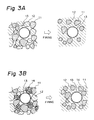
- Figure 3A schematically shows how this principle operates.
- a green sheet comprising alumina particles 11, borosilicate glass particles 12 and hollow glass microspheres 13
- the borosilicate glass particles 12 are fused or soften to form a matrix in which the alumina particles 11 and the hollow glass microspheres 13 are dispersed.
- the presence of the hollow glass microspheres 13 in the green sheet minimizes the shrinkage of the sheet.
- the green sheet for the signal layer comprises porous silica particles 14 in addition to alumina particles 11, borosilicate glass particles 12 and hollow glass microspheres 13, the large shrinkage of the porous silica particles 14 suffered during firing, as shown in Figure 3B or Figure 4, can be compensated for by the low shrinkage factor of the hollow glass microspheres 13 as shown in Figure 5, and therefor the overall firing shrinkage factor of the resulting green sheet can be made to coincide with that of a green sheet comprising alumina particles 11 and borosilicate particles 12 and free of hollow fine glass spheres 13 as shown in Figure 6.
- porous glass particles to be used in the practice of this invention include those obtained by the sol-gel method, i.e., those obtained by hydrolyzing silicone alkoxides such as tetramethoxy silicate [Si(OCH 3 )] and tetraethoxy silicate [Si(OC 2 H 5 ) 4] , which are prepared by reacting water glass with alcohols to give hydrated oxide sols, subjecting the sols to dehydration to form gels, and then heating the gels to form amorphous Si0 2.
- the porous silica is an aggregate of the fine particles of silica and had during firing, a high shrinkage factor in relation to the pores present therein.
- the porous glass also can be prepared by forming a glass in which sodium is dispersed In a glass matrix,and then leaching out the sodium phase.
- the ceramic particles used in the present invention are added to the green sheets to improve the mechanical strength of the resulting substrate and stabilize the glass (while also possibly preventing crystallization of the glass).
- Typical examples of ceramic particles are particles of alumina type such as mullite.
- a glass-type material such as silica, which is not softened at the firing temperature.
- the particle size of the ceramic particles is not critical in the present invention, but those having a particle size of from 2 to 3 f..lm are usually employed.
- the amount of the ceramic (alumina etc.) particles to be incorporated ranges from 10 to 70 % by weight related to the total weight of the inorganic materials for preparing the glass ceramic component of the green sheets, which particles comprise the ceramic particles or high softening point glass particles, hollow glass microspheres, glass particles and porous glass particles, with a part of the ceramic particles being replaced by hollow glass microspheres.
- the upper limit to the amount of the hollow glass microspheres to be incorporated is of the order of 40% by weight, based on the total weight of the inorganic materials.
- the hollow glass microspheres are added to the material to reduce the dielectric constant of the resulting glass ceramic layer formed by sintering the green sheet.
- the size of the microspheres is preferably as small as possible, and those having a particle size of not less than 10 f..lm are readily available on the market.
- the low softening point glass is a glass capable of being softened at a temperature of not more than the firing temperature, and a typical example thereof usable in the invention is a borosilicate glass having a softening point of about 800°C.
- the amount of the low softening point glass used is preferably approximately equal to half of the remaining portion of the inorganic materials (30 to 90 % by weight) other than the ceramic particles and the hollow glass microspheres and in general ranges from 15 to 50 % by weight, with the balance being made up of the porous glass powders.
- Both the low softening point glass particles and the porous glass particles to be used in the invention preferably have a particle size of about 2 to 3 ⁇ m.
- the amount of porous glass powder to be incorporated in the inorganic material is such that the difference between the firing shrinkage factors of the green sheet comprising the ceramic particles and the low softening point glass particles and free of the hollow glass microspheres and of the green sheet comprising the ceramic particles, low softening point glass particles, hollow glass microspheres and porous glass powders is preferably not more than ⁇ 0.5%, more preferably not more than ⁇ 0.2%, as determined for a sheet having a size, for example of 300 mm 2 .
- the dielectric constants are 10 for the alumina, 4.6 for the borosilicate glass, about 1.3 for the hollow glass microspheres and 3.8 for the porous silica respectively.
- a conventional glass ceramic substrate comprising alumina, borosilicate glass and silica glass has a dielectric constant of 5 to 6, and such a substrate containing additionally, hollow glass microsphere has a dielectric constant of about 4 to 2.5.
- a multi-layer glass ceramic substrate can be manufactured by adding additives such as a binder, a solvent and/or a plasticizer to a mixture of ceramic particles, low softening point glass particles, hollow glass microspheres and porous glass powder, and kneading the resulting mixture to form a slurry; forming the slurry into green sheets (A); patterning signal distributing wires on the green sheets and laminating the green sheets to form a signal layer (B); separately forming green sheets (C) mainly comprising ceramic particles and glass particles; sandwiching the laminated signal layer (B) between upper and lower green sheets (C) to unite these layers; and then firing the resulting laminate.
- additives such as a binder, a solvent and/or a plasticizer
- the firing can be performed in a nitrogen gas atmosphere when the conductive material used is copper or in airwhen it is gold or an alloy of silver and palladium. More specifically, when the conductive material is copper, the firing temperature for the laminate is raised to about 850°C at a temperature elevation rate of about 50°C/hr, the temperature rise occurring in a wet nitrogen atmosphere, and the laminate is maintained at about 850°C over 4 hours. The temperature is then raised to 1000°C with the laminate blanketed by a dry nitrogen atmosphere,the temperature of the laminate is maintained at about 1000°C for 4 hours, and then the laminate is cooled.
- the layers free of hollow glass microspheres arranged on and below the signal layer serve to impart mechanical strength and evenness to the resulting multi-layer substrate. Also the upper and lower surfaces of the substrate can be ground to improve the evenness thereof.
- the following ingredients were mixed and kneaded to form a slurry, which was subjected to a degassing and formation therefrom of a green sheet having a thickness of 300 f..lm by means of the doctor blade process.
- the slurry had the composition:
- the green sheet was then formed into pieces 9 x 9 cm, by blanking, and subsequently, a copper (Cu) paste was applied to the surface thereof to form lines of conductive material by a screen printing process.
- Cu copper
- the resulting substrate had a firing shrinkage factor of 18%. Namely, the firing shrinkage factor was 2% higher than that (16%) of the conventional multi-layer substrate free of the porous silica glass powder.
- the green sheet was formed into pieces 9 x 9 cm by blanking,to give green sheets for use in producing a signal layer, and subsequently, a copper (Cu) paste was applied to the surfaces of eight of these green sheets to form lines of the conductive material, by a screen printing process.
- Cu copper
- the green sheet was formed into pieces 9 x 9 cm, by blanking,to give green sheets for use as reinforcing layers.
- each of the green sheets for the reinforcing layer was placed as an upper or lower surface of each green sheet for the signal layer (8 sheets in all),the sheets then were stacked, a pressure of 10 MPa was applied to the resulting laminate at 80°C, to unite the laminate ad the united laminate was then fired at 1000°C for 5 hours to give a multi-layer substrate.
- Figure 5 shows the firing shrinkage factor curves of the foregoing green sheet for the reinforcing layer and a conventional hollow silica microspheres-containing green sheet, which has the same composition as that of the foregoing green sheet for a signal layer except for replacing all of the porous silica glass powder with hollow silica microspheres.
- the former has a firing shrinkage factor of 18% and the latter has a shrinkage factor of 13%, and hence,the difference in the firing shrinkage factors is as much as 5%. Therefore, if these green sheets are assembled together and united, the multi-layer substrate obtained after firing suffers from the problems of cracking and delamination as shown in Figure 7.
- reference numerals 21 and 22 represent a signal layer and a reinforcing layer respectively, Figure 7 showing these layers in the green sheet state (upper) and sintered glass ceramic layer state (lower).
- Figure 6 shows the firing shrinkage factor curves of a green sheet for the reinforcing layer and for the signal layer (comprising hollow silica microspheres and porous silica glass powders) obtained in the foregoing example.
- the curves shown in Figure 6 indicate that the shrinkage behaviour of the reinforcing layer closely matches that observed for the signal layer.
Landscapes
- Chemical & Material Sciences (AREA)
- Engineering & Computer Science (AREA)
- Ceramic Engineering (AREA)
- Materials Engineering (AREA)
- Structural Engineering (AREA)
- Organic Chemistry (AREA)
- Production Of Multi-Layered Print Wiring Board (AREA)
- Compositions Of Oxide Ceramics (AREA)
Applications Claiming Priority (2)
| Application Number | Priority Date | Filing Date | Title |
|---|---|---|---|
| JP3079457A JPH04314394A (ja) | 1991-04-12 | 1991-04-12 | ガラスセラミック回路基板とその製造方法 |
| JP79457/91 | 1991-04-12 |
Publications (2)
| Publication Number | Publication Date |
|---|---|
| EP0508821A2 true EP0508821A2 (de) | 1992-10-14 |
| EP0508821A3 EP0508821A3 (en) | 1993-10-13 |
Family
ID=13690412
Family Applications (1)
| Application Number | Title | Priority Date | Filing Date |
|---|---|---|---|
| EP19920303245 Withdrawn EP0508821A3 (en) | 1991-04-12 | 1992-04-10 | Process for manufacturing multi-layer glass ceramic substrate |
Country Status (5)
| Country | Link |
|---|---|
| US (1) | US5458709A (de) |
| EP (1) | EP0508821A3 (de) |
| JP (1) | JPH04314394A (de) |
| KR (1) | KR950000693B1 (de) |
| CA (1) | CA2065537C (de) |
Cited By (1)
| Publication number | Priority date | Publication date | Assignee | Title |
|---|---|---|---|---|
| WO2008043320A1 (de) * | 2006-10-11 | 2008-04-17 | Kerafol Keramische Folien Gmbh | Verfahren zur herbeiführung eines definierten schrumpfungsverhaltens eines keramischen grünfolienabschnittes |
Families Citing this family (21)
| Publication number | Priority date | Publication date | Assignee | Title |
|---|---|---|---|---|
| JP3223199B2 (ja) * | 1991-10-25 | 2001-10-29 | ティーディーケイ株式会社 | 多層セラミック部品の製造方法および多層セラミック部品 |
| JPH0645759A (ja) * | 1992-07-22 | 1994-02-18 | Fujitsu Ltd | 多層セラミック回路基板の製造方法 |
| US6258191B1 (en) * | 1998-09-16 | 2001-07-10 | International Business Machines Corporation | Method and materials for increasing the strength of crystalline ceramic |
| US6214746B1 (en) * | 1999-05-07 | 2001-04-10 | Honeywell International Inc. | Nanoporous material fabricated using a dissolvable reagent |
| US6171687B1 (en) | 1999-10-18 | 2001-01-09 | Honeywell International Inc. | Infiltrated nanoporous materials and methods of producing same |
| US20040176488A1 (en) * | 2000-06-06 | 2004-09-09 | Shyama Mukherjee | Low dielectric materials and methods of producing same |
| US6444715B1 (en) | 2000-06-06 | 2002-09-03 | Honeywell International Inc. | Low dielectric materials and methods of producing same |
| US6627669B2 (en) | 2000-06-06 | 2003-09-30 | Honeywell International Inc. | Low dielectric materials and methods of producing same |
| US7049386B2 (en) | 2000-07-19 | 2006-05-23 | Honeywell International Inc. | Compositions and methods for thermosetting molecules in organic compositions |
| US20020022708A1 (en) | 2000-07-19 | 2002-02-21 | Honeywell International Inc. | Compositions and methods for thermosetting molecules in organic compositions |
| US6469123B1 (en) | 2000-07-19 | 2002-10-22 | Honeywell International Inc. | Compositions and methods for thermosetting molecules in organic compositions |
| US6423811B1 (en) | 2000-07-19 | 2002-07-23 | Honeywell International Inc. | Low dielectric constant materials with polymeric networks |
| US20040102584A1 (en) * | 2001-12-03 | 2004-05-27 | Lau Kreisler S. | Low dielectric constant materials with polymeric networks |
| JP3847628B2 (ja) * | 2002-01-09 | 2006-11-22 | 株式会社ワコム | 低電圧駆動回路及び方法 |
| JP2006240020A (ja) * | 2005-03-02 | 2006-09-14 | Fuji Photo Film Co Ltd | 液体吐出ヘッド及び液体吐出ヘッドの製造方法 |
| US20070090545A1 (en) * | 2005-10-24 | 2007-04-26 | Condie Brian W | Semiconductor device with improved encapsulation |
| US7432133B2 (en) * | 2005-10-24 | 2008-10-07 | Freescale Semiconductor, Inc. | Plastic packaged device with die interface layer |
| US7435625B2 (en) * | 2005-10-24 | 2008-10-14 | Freescale Semiconductor, Inc. | Semiconductor device with reduced package cross-talk and loss |
| US20180035549A1 (en) * | 2015-01-13 | 2018-02-01 | Ngk Spark Plug Co., Ltd. | Circuit board and production method therefor |
| US20230317592A1 (en) * | 2022-04-01 | 2023-10-05 | Intel Corporation | Substrate with low-permittivity core and buildup layers |
| CN117303868A (zh) * | 2023-09-22 | 2023-12-29 | 香港科技大学(广州) | 一种低介电常数、高弯曲强度的氧化铝陶瓷材料的制备方法 |
Family Cites Families (10)
| Publication number | Priority date | Publication date | Assignee | Title |
|---|---|---|---|---|
| JPS599992A (ja) * | 1982-07-08 | 1984-01-19 | 株式会社日立製作所 | 多層配線基板の製造方法 |
| US4840653A (en) * | 1983-12-22 | 1989-06-20 | American Telephone And Telegraph Company, At&T Bell Laboratories | Fabrication of high-silica glass article |
| JPS60254697A (ja) * | 1984-05-31 | 1985-12-16 | 富士通株式会社 | 多層セラミック回路基板および製法 |
| JPS6112091A (ja) * | 1984-06-27 | 1986-01-20 | 株式会社日立製作所 | 多層回路基板及びその製造方法 |
| JPS6183674A (ja) * | 1984-10-01 | 1986-04-28 | 株式会社日立製作所 | セラミツク配線基板及びその製造方法 |
| US4865875A (en) * | 1986-02-28 | 1989-09-12 | Digital Equipment Corporation | Micro-electronics devices and methods of manufacturing same |
| JPS62287658A (ja) * | 1986-06-06 | 1987-12-14 | Hitachi Ltd | セラミックス多層回路板 |
| US4867935A (en) * | 1988-02-26 | 1989-09-19 | E. I. Du Pont De Nemours And Company | Method for preparing ceramic tape compositions |
| DK0432907T3 (da) * | 1989-11-22 | 1995-07-10 | Johnson Matthey Plc | Forbedrede pastasammensætninger |
| JP2906282B2 (ja) * | 1990-09-20 | 1999-06-14 | 富士通株式会社 | ガラスセラミック・グリーンシートと多層基板、及び、その製造方法 |
-
1991
- 1991-04-12 JP JP3079457A patent/JPH04314394A/ja active Pending
-
1992
- 1992-04-07 CA CA002065537A patent/CA2065537C/en not_active Expired - Fee Related
- 1992-04-10 EP EP19920303245 patent/EP0508821A3/en not_active Withdrawn
- 1992-04-13 US US07/867,513 patent/US5458709A/en not_active Expired - Fee Related
- 1992-04-13 KR KR1019920006137A patent/KR950000693B1/ko not_active Expired - Fee Related
Cited By (1)
| Publication number | Priority date | Publication date | Assignee | Title |
|---|---|---|---|---|
| WO2008043320A1 (de) * | 2006-10-11 | 2008-04-17 | Kerafol Keramische Folien Gmbh | Verfahren zur herbeiführung eines definierten schrumpfungsverhaltens eines keramischen grünfolienabschnittes |
Also Published As
| Publication number | Publication date |
|---|---|
| US5458709A (en) | 1995-10-17 |
| KR920019708A (ko) | 1992-11-19 |
| CA2065537C (en) | 1996-04-09 |
| EP0508821A3 (en) | 1993-10-13 |
| CA2065537A1 (en) | 1992-10-13 |
| KR950000693B1 (ko) | 1995-01-27 |
| JPH04314394A (ja) | 1992-11-05 |
Similar Documents
| Publication | Publication Date | Title |
|---|---|---|
| US5458709A (en) | Process for manufacturing multi-layer glass ceramic substrate | |
| US5593526A (en) | Process for preparing a multi-layer wiring board | |
| EP0211619B1 (de) | Keramische Mehrschichtschaltungsplatte | |
| US4821142A (en) | Ceramic multilayer circuit board and semiconductor module | |
| EP0345809B1 (de) | Mehrschichtige keramische Platine, Verfahren zu ihrer Herstellung und ihre Anwendung | |
| US5071793A (en) | Low dielectric inorganic composition for multilayer ceramic package | |
| US5714112A (en) | Process for producing a silica sintered product for a multi-layer wiring substrate | |
| US5206190A (en) | Dielectric composition containing cordierite and glass | |
| JPS63358A (ja) | 超小型電子技術装置の製造に使用する誘電率の低い材料、及びその製造方法 | |
| JP2001060767A (ja) | セラミック基板の製造方法および未焼成セラミック基板 | |
| EP0532842A1 (de) | Schwach dielektrische anorganische Zusammensetzung für eine mehrschichtige keramische Einheit | |
| EP0575813B1 (de) | Glaskeramisches Mehrschichtsubstrat und Verfahren zur seiner Herstellung | |
| JPH0811696B2 (ja) | 多層ガラスセラミック基板とその製造方法 | |
| EP0476954B1 (de) | Verfahren zum Herstellen von Grünfolien | |
| JP2787026B2 (ja) | 低誘電率多層セラミック回路基盤の製造方法 | |
| US5283210A (en) | Low temperature sintering low dielectric inorganic composition | |
| JP3166850B2 (ja) | 低温焼成ガラスセラミックスとその製造方法 | |
| KR102964440B1 (ko) | 적층 유리 세라믹 유전체 재료, 소결체, 소결체의 제조 방법 및 고주파용 회로 부재 | |
| JPH06120633A (ja) | セラミック配線基板 | |
| JPH0766563A (ja) | 容量内蔵型多層回路基板 | |
| KR0173233B1 (ko) | 저유전율 다층 세라믹 회로기판의 제조방법 | |
| JP3047985B2 (ja) | 多層セラミック配線基板の製造方法 | |
| JP2504350B2 (ja) | 多層ガラスセラミック基板とその製造方法 | |
| JP2504351B2 (ja) | 多層ガラスセラミック基板とその製造方法 | |
| JP2723710B2 (ja) | 多層ガラスセラミック基板及びその製造方法 |
Legal Events
| Date | Code | Title | Description |
|---|---|---|---|
| PUAI | Public reference made under article 153(3) epc to a published international application that has entered the european phase |
Free format text: ORIGINAL CODE: 0009012 |
|
| AK | Designated contracting states |
Kind code of ref document: A2 Designated state(s): DE FR GB |
|
| PUAL | Search report despatched |
Free format text: ORIGINAL CODE: 0009013 |
|
| RHK1 | Main classification (correction) |
Ipc: H01L 21/48 |
|
| AK | Designated contracting states |
Kind code of ref document: A3 Designated state(s): DE FR GB |
|
| 17P | Request for examination filed |
Effective date: 19940407 |
|
| 17Q | First examination report despatched |
Effective date: 19950906 |
|
| STAA | Information on the status of an ep patent application or granted ep patent |
Free format text: STATUS: THE APPLICATION IS DEEMED TO BE WITHDRAWN |
|
| 18D | Application deemed to be withdrawn |
Effective date: 19971101 |