EP0510541B1 - Organische elektroluminescente Vorrichtung - Google Patents
Organische elektroluminescente Vorrichtung Download PDFInfo
- Publication number
- EP0510541B1 EP0510541B1 EP92106677A EP92106677A EP0510541B1 EP 0510541 B1 EP0510541 B1 EP 0510541B1 EP 92106677 A EP92106677 A EP 92106677A EP 92106677 A EP92106677 A EP 92106677A EP 0510541 B1 EP0510541 B1 EP 0510541B1
- Authority
- EP
- European Patent Office
- Prior art keywords
- organic
- electroluminescent device
- organic electroluminescent
- group
- injection transport
- Prior art date
- Legal status (The legal status is an assumption and is not a legal conclusion. Google has not performed a legal analysis and makes no representation as to the accuracy of the status listed.)
- Expired - Lifetime
Links
Images

Classifications
-
- H—ELECTRICITY
- H05—ELECTRIC TECHNIQUES NOT OTHERWISE PROVIDED FOR
- H05B—ELECTRIC HEATING; ELECTRIC LIGHT SOURCES NOT OTHERWISE PROVIDED FOR; CIRCUIT ARRANGEMENTS FOR ELECTRIC LIGHT SOURCES, IN GENERAL
- H05B33/00—Electroluminescent light sources
- H05B33/12—Light sources with substantially two-dimensional [2D] radiating surfaces
- H05B33/26—Light sources with substantially two-dimensional [2D] radiating surfaces characterised by the composition or arrangement of the conductive material used as an electrode
-
- C—CHEMISTRY; METALLURGY
- C09—DYES; PAINTS; POLISHES; NATURAL RESINS; ADHESIVES; COMPOSITIONS NOT OTHERWISE PROVIDED FOR; APPLICATIONS OF MATERIALS NOT OTHERWISE PROVIDED FOR
- C09K—MATERIALS FOR MISCELLANEOUS APPLICATIONS, NOT PROVIDED FOR ELSEWHERE
- C09K11/00—Luminescent materials, e.g. electroluminescent or chemiluminescent
- C09K11/06—Luminescent materials, e.g. electroluminescent or chemiluminescent containing organic luminescent materials
-
- H—ELECTRICITY
- H05—ELECTRIC TECHNIQUES NOT OTHERWISE PROVIDED FOR
- H05B—ELECTRIC HEATING; ELECTRIC LIGHT SOURCES NOT OTHERWISE PROVIDED FOR; CIRCUIT ARRANGEMENTS FOR ELECTRIC LIGHT SOURCES, IN GENERAL
- H05B33/00—Electroluminescent light sources
- H05B33/12—Light sources with substantially two-dimensional [2D] radiating surfaces
-
- H—ELECTRICITY
- H05—ELECTRIC TECHNIQUES NOT OTHERWISE PROVIDED FOR
- H05B—ELECTRIC HEATING; ELECTRIC LIGHT SOURCES NOT OTHERWISE PROVIDED FOR; CIRCUIT ARRANGEMENTS FOR ELECTRIC LIGHT SOURCES, IN GENERAL
- H05B33/00—Electroluminescent light sources
- H05B33/12—Light sources with substantially two-dimensional [2D] radiating surfaces
- H05B33/14—Light sources with substantially two-dimensional [2D] radiating surfaces characterised by the chemical or physical composition or the arrangement of the electroluminescent material, or by the simultaneous addition of the electroluminescent material in or onto the light source
-
- H—ELECTRICITY
- H10—SEMICONDUCTOR DEVICES; ELECTRIC SOLID-STATE DEVICES NOT OTHERWISE PROVIDED FOR
- H10K—ORGANIC ELECTRIC SOLID-STATE DEVICES
- H10K50/00—Organic light-emitting devices
- H10K50/10—OLEDs or polymer light-emitting diodes [PLED]
- H10K50/11—OLEDs or polymer light-emitting diodes [PLED] characterised by the electroluminescent [EL] layers
-
- H—ELECTRICITY
- H10—SEMICONDUCTOR DEVICES; ELECTRIC SOLID-STATE DEVICES NOT OTHERWISE PROVIDED FOR
- H10K—ORGANIC ELECTRIC SOLID-STATE DEVICES
- H10K50/00—Organic light-emitting devices
- H10K50/10—OLEDs or polymer light-emitting diodes [PLED]
- H10K50/14—Carrier transporting layers
- H10K50/15—Hole transporting layers
- H10K50/155—Hole transporting layers comprising dopants
-
- H—ELECTRICITY
- H10—SEMICONDUCTOR DEVICES; ELECTRIC SOLID-STATE DEVICES NOT OTHERWISE PROVIDED FOR
- H10K—ORGANIC ELECTRIC SOLID-STATE DEVICES
- H10K50/00—Organic light-emitting devices
- H10K50/10—OLEDs or polymer light-emitting diodes [PLED]
- H10K50/17—Carrier injection layers
-
- H—ELECTRICITY
- H10—SEMICONDUCTOR DEVICES; ELECTRIC SOLID-STATE DEVICES NOT OTHERWISE PROVIDED FOR
- H10K—ORGANIC ELECTRIC SOLID-STATE DEVICES
- H10K50/00—Organic light-emitting devices
- H10K50/10—OLEDs or polymer light-emitting diodes [PLED]
- H10K50/17—Carrier injection layers
- H10K50/171—Electron injection layers
-
- H—ELECTRICITY
- H10—SEMICONDUCTOR DEVICES; ELECTRIC SOLID-STATE DEVICES NOT OTHERWISE PROVIDED FOR
- H10K—ORGANIC ELECTRIC SOLID-STATE DEVICES
- H10K85/00—Organic materials used in the body or electrodes of devices covered by this subclass
- H10K85/30—Coordination compounds
-
- H—ELECTRICITY
- H10—SEMICONDUCTOR DEVICES; ELECTRIC SOLID-STATE DEVICES NOT OTHERWISE PROVIDED FOR
- H10K—ORGANIC ELECTRIC SOLID-STATE DEVICES
- H10K85/00—Organic materials used in the body or electrodes of devices covered by this subclass
- H10K85/30—Coordination compounds
- H10K85/321—Metal complexes comprising a group IIIA element, e.g. Tris (8-hydroxyquinoline) gallium [Gaq3]
-
- H—ELECTRICITY
- H10—SEMICONDUCTOR DEVICES; ELECTRIC SOLID-STATE DEVICES NOT OTHERWISE PROVIDED FOR
- H10K—ORGANIC ELECTRIC SOLID-STATE DEVICES
- H10K85/00—Organic materials used in the body or electrodes of devices covered by this subclass
- H10K85/30—Coordination compounds
- H10K85/321—Metal complexes comprising a group IIIA element, e.g. Tris (8-hydroxyquinoline) gallium [Gaq3]
- H10K85/324—Metal complexes comprising a group IIIA element, e.g. Tris (8-hydroxyquinoline) gallium [Gaq3] comprising aluminium, e.g. Alq3
-
- H—ELECTRICITY
- H10—SEMICONDUCTOR DEVICES; ELECTRIC SOLID-STATE DEVICES NOT OTHERWISE PROVIDED FOR
- H10K—ORGANIC ELECTRIC SOLID-STATE DEVICES
- H10K85/00—Organic materials used in the body or electrodes of devices covered by this subclass
- H10K85/60—Organic compounds having low molecular weight
-
- H—ELECTRICITY
- H10—SEMICONDUCTOR DEVICES; ELECTRIC SOLID-STATE DEVICES NOT OTHERWISE PROVIDED FOR
- H10K—ORGANIC ELECTRIC SOLID-STATE DEVICES
- H10K85/00—Organic materials used in the body or electrodes of devices covered by this subclass
- H10K85/60—Organic compounds having low molecular weight
- H10K85/611—Charge transfer complexes
-
- H—ELECTRICITY
- H10—SEMICONDUCTOR DEVICES; ELECTRIC SOLID-STATE DEVICES NOT OTHERWISE PROVIDED FOR
- H10K—ORGANIC ELECTRIC SOLID-STATE DEVICES
- H10K85/00—Organic materials used in the body or electrodes of devices covered by this subclass
- H10K85/60—Organic compounds having low molecular weight
- H10K85/615—Polycyclic condensed aromatic hydrocarbons, e.g. anthracene
-
- H—ELECTRICITY
- H10—SEMICONDUCTOR DEVICES; ELECTRIC SOLID-STATE DEVICES NOT OTHERWISE PROVIDED FOR
- H10K—ORGANIC ELECTRIC SOLID-STATE DEVICES
- H10K85/00—Organic materials used in the body or electrodes of devices covered by this subclass
- H10K85/60—Organic compounds having low molecular weight
- H10K85/615—Polycyclic condensed aromatic hydrocarbons, e.g. anthracene
- H10K85/621—Aromatic anhydride or imide compounds, e.g. perylene tetra-carboxylic dianhydride or perylene tetracarboxylic di-imide
-
- H—ELECTRICITY
- H10—SEMICONDUCTOR DEVICES; ELECTRIC SOLID-STATE DEVICES NOT OTHERWISE PROVIDED FOR
- H10K—ORGANIC ELECTRIC SOLID-STATE DEVICES
- H10K85/00—Organic materials used in the body or electrodes of devices covered by this subclass
- H10K85/60—Organic compounds having low molecular weight
- H10K85/631—Amine compounds having at least two aryl rest on at least one amine-nitrogen atom, e.g. triphenylamine
-
- H—ELECTRICITY
- H10—SEMICONDUCTOR DEVICES; ELECTRIC SOLID-STATE DEVICES NOT OTHERWISE PROVIDED FOR
- H10K—ORGANIC ELECTRIC SOLID-STATE DEVICES
- H10K85/00—Organic materials used in the body or electrodes of devices covered by this subclass
- H10K85/60—Organic compounds having low molecular weight
- H10K85/649—Aromatic compounds comprising a hetero atom
-
- H—ELECTRICITY
- H10—SEMICONDUCTOR DEVICES; ELECTRIC SOLID-STATE DEVICES NOT OTHERWISE PROVIDED FOR
- H10K—ORGANIC ELECTRIC SOLID-STATE DEVICES
- H10K85/00—Organic materials used in the body or electrodes of devices covered by this subclass
- H10K85/60—Organic compounds having low molecular weight
- H10K85/649—Aromatic compounds comprising a hetero atom
- H10K85/656—Aromatic compounds comprising a hetero atom comprising two or more different heteroatoms per ring
- H10K85/6565—Oxadiazole compounds
Definitions
- the present invention relates to an organic electroluminescent device. More particularly, it relates to a thin-film type device comprising a combination of a hole injection transport layer and a luminescent layer made of organic compounds, respectively, which is designed to emit light upon application of an electric field.
- US-A-4 769 292 discloses an organic electroluminescent device with a hole injection transport layer containing copper phthalocyanine complexes.
- US-A-4 720 432 discloses an organic electroluminescent device with a hole injection transport layer containing chromium or zirconium phthalocyanine complexes.
- thin-film type electroluminescent devices are made of inorganic material which is obtained by doping a semiconductor of a Group II-VI compound such as ZnS, CaS or SrS with Mn or a rare earth element (such as Eu, Ce, Tb or Sm) as the luminous center.
- a semiconductor of a Group II-VI compound such as ZnS, CaS or SrS with Mn or a rare earth element (such as Eu, Ce, Tb or Sm) as the luminous center.
- the electroluminescent devices prepared from such inorganic materials have problems such that 1) alternate current driving is required (about 1 KHz), 2) the driving voltage is high (about 200 V), 3) it is difficult to obtain full coloring, and 4) the cost for peripheral driving circuits is high.
- electroluminescence is brought about by recombination of injected holes and electrons.
- injection of a carrier has to be conducted by overcoming an injection barrier at the interface between the anode and the organic hole injection transport layer in the case of holes, or by overcoming a barrier at the interface between the cathode and the luminescent layer in the case of electrons. Therefore, a high electric field is required for the injection. Accordingly, the driving voltage for the device is required to be high, and the luminous performance, particularly the luminous efficiency, tends to be inadequate. Further, instability of the operation due to instability of the interface is observed. Therefore, further improvements have been desired.
- the present invention provides an organic electroluminescent device having an anode, an organic hole injection transport layer, an organic luminescent layer and a cathode formed sequentially in this order, wherein the organic hole injection transport layer contains a metal complex and/or a metal salt of an aromatic carboxylic acid of the formula (I) Ar COOH, wherein Ar is a substituted or unsubstituted aromatic ring or aromatic heterocyclic ring residue.
- the present inventors have conducted extensive studies for an organic electroluminescent device which can be driven at a low voltage and as a result, have found it effective to incorporate a certain specific compound to the organic hole injection transport layer.
- the present invention has been accomplished on the basis of this discovery.
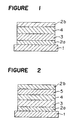
- Figure 1 is a cross sectional view showing an embodiment of the organic electroluminescent device of the present invention.
- Figure 2 is a cross sectional view showing another embodiment of the organic electroluminescent device of the present invention.
- Figure 3 is a graph showing the luminance-voltage characteristics of devices A and C.
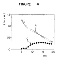
- Figure 4 is a graph showing the luminous efficiency-voltage characteristics of devices A and C.
- reference numeral 1 indicates a substrate
- numerals 2a and 2b indicate conductive layers
- numeral 3 indicates an organic hole injection transport layer
- numeral 4 indicates an organic luminescent layer.
- the substrate 1 constitutes a support for the electroluminescent device of the present invention and may be made of a quartz or glass sheet, a metal sheet or foil, or a plastic film or sheet. However, it is preferred to employ a glass sheet or a substrate made of a transparent synthetic resin such as polyester, polymethacrylate, polycarbonate or polysulfone.
- a conductive layer 2a is provided on the substrate 1.
- Such a conductive layer 2a is usually made of a metal such as aluminum, gold, silver, nickel, palladium or tellurium, a metal oxide such as an oxide of indium and/or tin, copper iodide, carbon black or a conductive resin such as poly(3-methylthiophene).
- the conductive layer 2a plays a hole injection role as an anode.
- the conductive layer 2b plays a role of injecting electrons to the luminescent layer 4 as a cathode.
- the material to be used as the conductive layer 2b the same material as mentioned above with respect to the conductive layer 2a, may be employed.
- a metal having a low value of work function it is preferred to employ a metal having a low value of work function.
- a suitable metal such as tin, magnesium, indium, aluminum or silver, or their alloys may be employed.
- the conductive layers 2a and 2b are usually formed by sputtering or vacuum deposition.
- a metal such as silver, copper iodide, carbon black
- fine particles of conductive metal oxide or fine conductive resin powder such material may be dispersed in a suitable binder resin solution and coated on a substrate to form the conductive layer.
- a conductive resin a thin film may directly be formed on a substrate by electrolytic polymerization.
- This conductive layer 2a or 2b may be made to have a multi-layered structure by depositing different types of materials among the above mentioned materials.
- the thickness of the conductive layer 2a varies depending upon the required transparency. When transparency is required, the transmittance of visible light is usually at least 60%, preferably at least 80%. In such a case, the thickness of the conductive layer is usually from 50 to 10,000 ⁇ (5-1000 nm), preferably from 100 to 5,000 ⁇ (10-500 nm).
- the material for the conductive layer 2a may be the same as the material for the substrate 1, or the conductive layer may be coated with a material different from the above-mentioned material for the conductive layer.
- the thickness of the conductive layer 2b is usually at the same level as the thickness of the conductive layer 2a.
- a substrate like the substrate 1 may further be provided on the conductive layer 2b.
- at least one of the conductive layers 2a and 2b is required to have good transparency for an electroluminescent device.
- one of the conductive layers 2a and 2b is desired to have good transparency preferably with a thickness of from 100 to 5,000 ⁇ (10-500 nm).
- an organic hole injection transport layer 3 is formed on the conductive layer 2a.
- the hole injection transport layer 3 is formed of a compound which is capable of efficiently transporting holes from the anode towards the organic luminescent layer between the electrodes to which an electric field is applied.
- Such a hole injection transport compound is required to be a compound having a high efficiency for injecting holes from the conductive layer 2a and being capable of efficiently transporting the injected holes.
- it is required to be a compound having a low ionization potential, large hole mobility and stability, whereby impurities likely to form traps, are scarcely formed during the preparation or use.
- Such a hole injection transport compound includes, for example, those disclosed on pages 5 and 6 in Japanese Unexamined Patent Publication No. 194393/1984 and in columns 13 and 14 in US Patent 4,175,960.
- Preferred specific examples of such a compound include aromatic amine compounds such as N,N′-diphenyl-N,N′-(3-methylphenyl)-1,1′-biphenyl-4,4′-diamine, 1,1′-bis(4-di-p-tolylaminophenyl)cyclohexane, and 4,4′-bis(diphenylamino)quadrophenyl.
- aromatic amine compounds such as N,N′-diphenyl-N,N′-(3-methylphenyl)-1,1′-biphenyl-4,4′-diamine, 1,1′-bis(4-di-p-tolylaminophenyl)cyclohexane, and 4,4′-bis(diphenylamino)quadropheny
- the organic hole injection transport layer 3 made of such an organic hole injection transport compound, contains a metal complex and/or a metal salt of an aromatic carboxylic acid, of the following formula (I): ArCOOH (I)
- Ar is an aromatic ring or aromatic heterocyclic ring residue which may have substituents.
- it may be an aromatic residue of e.g. benzene, naphthalene or anthracene, or an organic heterocyclic ring residue of e.g. carbazole, which may have substituents such as an alkyl group, an aryl group, a hydroxyl group, an alkoxy group, an aryloxy group, an alkylcarbonyl group, an arylcarbonyl group, an alkoxycarbonyl group, an aryloxycarbonyl group, a carboxyl group, a nitro group, a cyano group and a halogen atom.
- a hydroxyl group is preferred as the substituent for Ar.
- any metal capable of forming a metal salt or a metal complex with the above aromatic carboxylic acid may be employed.
- Particularly preferred is Al, Zn, Cr, Co, Ni or Fe.
- the metal complex or the metal salt of an aromatic carboxylic acid according to the present invention may be synthesized, for example, by a method disclosed in e.g. J. Am. Chem. Soc., Vol. 70, p2151 (1948), Japanese Unexamined Patent Publication No. 127726/1978, No. 104940/1982, No. 42752/1980 or No. 79256/1984.
- a methanol solution of 3,5-di-tert-butylsalicylic acid and an aqueous solution of Cr2(SO4)3 are mixed, the pH is adjusted to a level of from 4 to 5 by an aqueous sodium hydroxide solution, followed by refluxing to obtain a chromium complex as slightly green precipitate.
- the desired compound may be prepared in accordance with this method.
- the resulting chromium complex of 3,5-di-tert-butylsalicylic acid is believed to have the following structural formula (B):
- the metal complex and/or the metal salt of an aromatic carboxylic acid of the above formula (I) is doped in an aromatic amine compound or a hydrazone compound as host material, to form an organic hole injection transport layer 3.
- the amount of the metal complex and/or the metal salt of an organic carboxylic acid to be doped in the host material is preferably from 10 ⁇ 3 to 10 mol%.
- the region to be doped may be the entire region of the organic hole injection transport layer or a part thereof.
- the organic hole injection transport layer 3 containing such a metal complex and/or a metal salt of an aromatic carboxylic acid, is formed on the above-mentioned conductive layer 2a by a coating method or a vacuum deposition method.
- a coating solution is prepared by adding and dissolving one or more organic hole injection transport compounds, the metal complex and/or the metal salt of an aromatic carboxylic acid of the above formula (I) and, if necessary, a binder resin which will not trap holes and an additive such as a coating property-improving agent such as a leveling agent, and the coating solution is applied on the conductive layer 2a by a method such as a spin coating method, followed by drying to form the organic hole injection transport layer 3.
- a binder resin a polycarbonate, a polyarylate or a polyester may, for example, be mentioned. If the amount of the binder resin is large, the hole mobility tends to decrease. Therefore, the smaller the amount of the binder resin, the better.
- the amount is preferably at most 50% by weight relative to the coating solution.
- the organic hole injection transport compound is put into a crucible placed in a vacuum chamber, the metal complex and/or the metal salt of an aromatic carboxylic acid of the above formula (I) is put in another crucible, then the vacuum chamber is evacuated to a level of 10 ⁇ 6 Torr (133.3x10 ⁇ 6 Pa) by a suitable vacuum pump, and the respective crucibles are heated simultaneously to evaporate the contents and to form a layer on a substrate disposed to face the crucibles. Otherwise, the above materials are preliminarily mixed, and the mixture is put into a single common crucible, followed by evaporation.
- organic hole injection transport compound an aromatic amine compound or a hydrazone compound which will be described hereinafter, may be employed.
- the thickness of the organic hole injection transport layer 3 is usually from 100 to 3,000 ⁇ (10-300 nm), preferably from 300 to 1,000 ⁇ (30-100 nm).
- a vacuum deposition method is preferably employed usually to form such a thin film uniformly.
- An organic luminescent layer 4 is formed on the organic hole injection transport layer 3.
- Such an organic luminescent layer 4 is desired to be capable of transporting electrons from the cathode efficiently towards the organic hole injection transport layer between the electrodes to which an electric field is applied.
- the compound to be used for the organic luminescent layer 4 is required to be a compound having a high efficiency for injection of electrons from the conductive layer 2b and which is capable of efficiently transporting the injected electrons.
- it is required to be a compound having a high electron affinity, large electron mobility and excellent stability and which scarcely forms impurities during the production or use, which are likely to form traps.
- an aromatic compound such as tetraphenylbutadiene (Japanese Unexamined Patent Publication No. 51781/1982), a metal complex such as an aluminum complex of 8-hydroxyquinoline (Japanese Unexamined Patent Publication No. 194393/1984), a cyclopentadiene derivative (Japanese Unexamined Patent Publication No. 289675/1990), a perinone derivative (Japanese Unexamined Patent Publication No. 289676/1990), an oxadiazole derivative (Japanese Unexamined Patent Publication No. 216791/1990), a bisstyrylbenzene derivative (Japanese Unexamined Patent Publication No.
- the thickness of the organic luminescent layer 4 is usually from 30 to 2,000 ⁇ (3-200 nm), preferably from 100 to 1,000 ⁇ (10-100 nm).
- Such an organic luminescent layer 4 may be formed by the same method as used for the formation of the organic hole injection transport layer. However, a vacuum deposition method is usually employed.
- the structure of a device as shown in Figure 2 may be employed in order to further improve the luminous efficiency of the organic electroluminescent device.
- the organic luminescent layer 4 may be made of the above-mentioned material for the organic luminescent layer, and an organic electron injection transport layer 5 is further deposited thereon.
- a compound to be used for this organic electron injection transport layer 5 is required to be such that injection of electrons from the cathode is easy, and the ability of transporting electrons is large.
- a nitro-substituted fluorenone derivative such as a compound of the formula ka-5, a thiopyrandioxide derivative such as a compound of the formula ka-6, a diphenylquinone derivative such as a compound of the formula ka-7, a perylene tetracarboxylic acid derivative such as a compound of the formula ka-8 (Jpn. J. Appl. Phys., Vol. 27, L269, 1988), or an oxadiazole derivative such as a compound of the formula ka-9 (Appl. Phys. Lett. Vol. 55, p1489, 1980), may be mentioned.
- the thickness of such an organic electron injection transport layer 5 is usually from 100 to 2,000 ⁇ (10-200 nm), preferably from 300 to 1,000 ⁇ (30-100 nm).
- a structure opposite to the one shown in Figure 1 may be adopted. Namely, it is possible to adopt a structure in which a conductive layer 2b, an organic luminescent layer 4, an organic hole injection transport layer 3 and a conductive layer 2a are formed on the substrate in this order. As described above, it is also possible to provide the electroluminescent device of the present invention between two substrates, at least one of which has high transparency. Likewise, it is also possible to adopt a structure opposite to the one shown in Figure 2, i.e. a structure wherein a conductive layer 2b, an organic electron injection transport layer 5, an organic luminescent layer 4, an organic hole injection transport layer 3 and a conductive layer 2a are sequentially formed on the substrate in this order.
- ITO indium-tin oxide
- NA-40 glass manufactured by HOYA K.K., ITO film thickness: 1,200 ⁇ (120 nm) is at a level of 4.70 eV.
- measurement of the work function was conducted by an ultraviolet photoelectron analyzer (AC-1 Model) manufactured by Riken Keiki K.K.
- N,N′-diphenyl-N,N′-(3-methylphenyl)-1,1′-biphenyl-4,4′-diamine (hereinafter referred to simply as "TPD") (Jpn. J. Appl. Phys., Vol. 27, L269, 1988) being an aromatic diamine used to be employed for an organic hole injection transport layer, has a structure of the following formula ka-10. This compound was formed into a thin film by vacuum deposition, and its ionization potential was measured in the same manner by AC-1 and found to be 5.23 eV. Thus, the hole injection barrier in this case is considered to be 0.53 eV.
- the ionization potential of the aromatic diamine and the hydrazone compound is usually within a range of from 5.2 to 5.5 eV, whereby it requires a high electric field to overcome the hole injection barrier. Further, a voltage drop occurs at the interface of anode/organic hole injection transport layer, whereby Joule heating is localized at the interface during the operation of the device, thus causing instability or deterioration of the operation of the device.
- the above aromatic diamine or hydrazone compound is an insulator by itself and is believed to have no intrinsic carrier, unless a carrier is injected from an electrode.
- the metal complex and/or the metal salt of an organic carboxylic acid as a doping material for the organic hole injection transport layer of an organic electroluminescent device, formation of a carrier is made possible without injection from an electrode, whereby excellent luminescent characteristics, particularly a reduction of the driving voltage, can be accomplished.
- Organic electroluminescent devices having the structure as shown in Figure 1, were prepared by a following method.
- ITO indium-tin oxide
- the temperatures of the respective crucibles were controlled so that the temperature for the hydrazone mixture was within a range of from 230 to 240°C, and the temperature for the aluminum salt of the aromatic carboxylic acid (8) of the formula ka-1 was 160°C.
- the pressure during the vacuum deposition was 2 ⁇ 10 ⁇ 7 Torr (266.6x10 ⁇ 7 Pa), and the time for the vacuum deposition was two minutes and 30 seconds.
- an organic hole injection transport layer having a thickness of 515 ⁇ (51.5 nm) and having the aluminum salt of the aromatic carboxylic acid (8) of the formula ka-1 doped in an amount of 2.3 mol%, was obtained.
- the temperature of the crucible was controlled to be 280°C, and the pressure during the vacuum deposition was 5 ⁇ 10 ⁇ 7 Torr ( ⁇ 6.7x10 ⁇ 5Pa), and the time for the vacuum deposition was two minutes.
- an organic luminescent layer 4 having a thickness of 520 ⁇ (52nm) was obtained.
- an alloy electrode of magnesium and silver was formed by vacuum deposition in a film thickness of 1,500 ⁇ (150nm) coevaporation vapor deposition method.
- a molybdenum boat was employed, the pressure was 8 ⁇ 10 ⁇ 6 Torr ( ⁇ 1x10 ⁇ 3Pa) , and the time for the vacuum deposition was 8 minutes.
- the atomic ratio of magnesium to silver was within a range of from 10:1 to 10:2.
- an organic electroluminescent device B was prepared in the same manner as the device A except that the concentration of the aluminum salt of the aromatic carboxylic acid (8) of the formula ka-1 in the organic hole injection transport layer was changed to 7.4 mol%.
- the luminescent characteristics were measured by applying a direct current positive voltage to the ITO electrode (anode) and a direct current negative voltage to the magnesium-silver electrode (cathode) of the organic electroluminescent devices A and B thus obtained, and the results are shown in Table 1. Further, the luminance-voltage characteristics of the device A are shown in Figure 3, and the luminous efficiency-voltage characteristics are shown in Figure 4.
- the emission spectra of these devices A and B showed uniform green emission over from 500 to 600 nm.
- Vth indicates a voltage at which the luminance becomes 1 cd/m2
- the luminous efficiency is an efficiency at V100
- V100 indicates a voltage at which the luminance becomes 100 cd/m2.
- An organic electroluminescent device C was prepared in the same manner as in Example 1 except that no doping was conducted to the organic hole injection transport layer.
- the luminescent characteristics of this device were measured, and the results are shown in Table 1. Further, the luminance-voltage characteristics of this device C are shown in Figure 3, and the luminous efficiency-voltage characteristics are shown in Figure 4. From these results, it is evident that with the device C, the driving voltage is high and the luminous efficiency is low as compared with the device A of Example 1.
- the luminescent spectrum of this device C was the same as in Example 1.
- An organic electroluminescent device D was prepared in the same manner as in Example 1 except that 1.4 mol part of a zinc salt of the aromatic carboxylic acid (8) of the formula ka-1 was doped in the organic hole injection transport layer.
- the luminescent characteristics of this device are shown in Table 1.
- the luminescent characteristics of this device are shown in Table 1.
- An organic electroluminescent device F was prepared in the same manner as in Example 3 except that no doping was conducted to the organic hole injection transport layer. The luminescent characteristics of this device were measured, and the results are shown in Table 1. From Table 1, it is evident that with the device F, the driving voltage is high and the luminous efficiency is low as compared with the device E of Example 4.
- the organic electroluminescent device of the present invention has an anode, an organic hole injection transport layer, an organic luminescent layer and a cathode sequentially formed on a substrate in this order, and a certain specific compound is incorporated to the organic hole injection transport layer, whereby when voltage is applied to both electrodes, a light emission with practically sufficient luminance can be obtained at a low driving voltage.
- the electroluminescent device of the present invention is useful in the field of flat panel displays (such as a wall-hanging television) or may be applied to a light source utilizing a spontaneous light-emitter (such as a light source for a copying machine, or a backlight light source for liquid crystal displays or meters), a display board or a beacon light.
- a spontaneous light-emitter such as a light source for a copying machine, or a backlight light source for liquid crystal displays or meters
- a display board or a beacon light a spontaneous light-emitter
Landscapes
- Chemical & Material Sciences (AREA)
- Engineering & Computer Science (AREA)
- Materials Engineering (AREA)
- Physics & Mathematics (AREA)
- Optics & Photonics (AREA)
- Inorganic Chemistry (AREA)
- Organic Chemistry (AREA)
- Electroluminescent Light Sources (AREA)
- Luminescent Compositions (AREA)
Claims (10)
- Organische Elektrolumineszenzvorrichtung mit einer Anode, einer organischen Lochinjektionstransportschicht, einer organischen Lumineszenzschicht und einer Kathode, die nacheinander in dieser Reihenfolge gebildet werden, dadurch gekennzeichnet, daß die organische Lochinjektionstransportschicht einen Metallkomplex einer aromatischen Carbonsäure und/oder ein Metallsalz einer aromatischen Carbonsäure enthält, wobei die aromatische Carbonsäure eine Verbindung der allgemeinen Formel (I) ist:
ArCOOH (I)
wobei Ar ein substituierter oder unsubstituierter aromatischer Ring oder aromatischer heterozyklischer Ring ist. - Organische Elektrolumineszenzvorrichtung nach Anspruch 1, wobei die organische Lochinjektionstransportschicht eine organische Aminverbindung oder eine Hydrazonverbindung als Wirtsmaterial umfaßt und wobei bezogen auf das Wirtsmaterial 10⁻³-10 mol-% der aromatischen Carbonsäure und/oder des Metallsalzes einer aromatischen Carbonsäure in dem Wirtsmaterial eindotiert sind.
- Organische Elektrolumineszenzvorrichtung nach Anspruch 1, wobei Ar in der allgemeinen Formel (1) ein Benzol-, Naphtalin-, Anthracen-, oder Carbazolring ist, der substituiert sein kann mit einer Alkylgruppe, einer Arylgruppe, einer Hydroxylgruppe, einer Alkoxygruppe, einer Aryloxygruppe, einer Alkylcarbonylgruppe, einer Arylcarbonylgruppe, einer Alkoxycarbonylgruppe, einer Aryloxycarbonylgruppe, einer Carboxylgruppe, einer Nitrogruppe, einer Cyanogruppe oder einem Halogenatom.
- Organische Elektrolumineszenzvorrichtung nach Anspruch 1, wobei das Metall für den Metallkomplex und/oder das Metallsalz einer aromatischen Carbonsäure Al, Zn, Cr, Co, Ni, oder Fe ist.
- Organische Elektrolumineszenzvorrichtung nach Anspruch 1, wobei die Anode aus einem Metall hergestellt wird, wie Aluminium, Gold, Silber, Nickel, Palladium, oder Tellur, aus einem Metalloxid, wie Indium- und/oder Zinnoxid, aus Kupferjodid, Ruß oder einem leitfähigen Harz, wie Poly(3-methylthiophen) und wobei die Kathode hergestellt wird aus einem Metall, wie Zinn, Magnesium, Indium, Aluminium oder Silber, oder einer Legierung daraus.
- Organische Elektrolumineszenzvorrichtung nach Anspruch 2, wobei die aromatische Aminverbindung N,N′-Diphenyl-N,N′-(3-methylphenyl)-1,1′-biphenyl-4,4′-diamin, 1,1′-Bis(4-di-p-tolylaminophenyl)cyclohexan oder 4,4′-Bis(diphenylamino)-quadrophenyl ist.
- Organische Elektrolumineszenzvorrichtung nach Anspruch 1, wobei die organische Lumineszenzschicht Tetraphenylbutadien, einen Aluminiumkomplex mit 8-Hydroxychinolin, ein Cyclopentadienderivat, ein Perinonderivat, ein Oxadiazolderivat, ein Bisstyrylbenzolderivat, ein Perylenderivat, eine Cumarinverbindung, eine Verbindung der seltenen Erden oder eine Distyrylpyrazinverbindung enthält.
- Organische Elektrolumineszenzvorrichtung nach Anspruch 1, wobei die Anodeeine Dicke von 50 bis 10.000 Å (5-1.000 nm) aufweist, die Kathode eine Dicke von 50 bis 10.000 Å (5-1.000 nm) aufweist, die organische Lochinjektionstransportschicht eine Dicke von 100 bis 3.000 Å (10-300 nm) aufweist und die organische Lumineszenzschicht eine Dicke von 30 bis 2.000 Å (3-200 nm) aufweist.
- Organische Elektrolumineszenzvorrichtung nach Anspruch 1, wobei mindestens die Anode oder die Kathode eine Dicke von 100-5.000 Å (10-500 nm) auweisen.
- Organische Elektrolumineszenzvorrichtung nach Anspruch 1, wobei eine organische Lochinjektionstransportschicht einer Dicke von 100-2.000 Å (10-200 nm) zwischen die organische Lumineszenzschicht und die Kathode zwischengeschaltet ist.
Applications Claiming Priority (2)
| Application Number | Priority Date | Filing Date | Title |
|---|---|---|---|
| JP3088444A JP2998268B2 (ja) | 1991-04-19 | 1991-04-19 | 有機電界発光素子 |
| JP88444/91 | 1991-04-19 |
Publications (2)
| Publication Number | Publication Date |
|---|---|
| EP0510541A1 EP0510541A1 (de) | 1992-10-28 |
| EP0510541B1 true EP0510541B1 (de) | 1995-12-27 |
Family
ID=13942977
Family Applications (1)
| Application Number | Title | Priority Date | Filing Date |
|---|---|---|---|
| EP92106677A Expired - Lifetime EP0510541B1 (de) | 1991-04-19 | 1992-04-16 | Organische elektroluminescente Vorrichtung |
Country Status (4)
| Country | Link |
|---|---|
| US (1) | US5247226A (de) |
| EP (1) | EP0510541B1 (de) |
| JP (1) | JP2998268B2 (de) |
| DE (1) | DE69207053D1 (de) |
Cited By (9)
| Publication number | Priority date | Publication date | Assignee | Title |
|---|---|---|---|---|
| WO2006026399A1 (en) * | 2004-08-25 | 2006-03-09 | Audiovox Corporation | Rail system used to engage a media device in a vehicle |
| US7026079B2 (en) | 2002-08-22 | 2006-04-11 | Agfa Gevaert | Process for preparing a substantially transparent conductive layer configuration |
| US7118836B2 (en) | 2002-08-22 | 2006-10-10 | Agfa Gevaert | Process for preparing a substantially transparent conductive layer configuration |
| US7667669B2 (en) | 2000-10-27 | 2010-02-23 | Audiovox Corporation | Vehicle display device having a wireless transmitter |
| US7839355B2 (en) | 2000-10-27 | 2010-11-23 | Audiovox Corporation | Vehicle display device having a wireless transmitter |
| US9166178B2 (en) | 2009-09-18 | 2015-10-20 | Osram Oled Gmbh | Organic electronic device and dopant for doping an organic semiconducting matrix material |
| US10256422B2 (en) | 2014-09-30 | 2019-04-09 | Osram Oled Gmbh | Organic electronic component, use of a zinc complex as a p-dopant for organic electronic matrix materials |
| US10305047B2 (en) | 2012-06-06 | 2019-05-28 | Siemens Aktiengesellschaft | Main group metal complexes as p-dopants for organic electronic matrix materials |
| US11040988B2 (en) | 2014-09-30 | 2021-06-22 | Novaled Gmbh | Method for producing an organic electronic component, and organic electronic component |
Families Citing this family (55)
| Publication number | Priority date | Publication date | Assignee | Title |
|---|---|---|---|---|
| US5378519A (en) * | 1992-04-28 | 1995-01-03 | Canon Kabushiki Kaisha | Electroluminescent device |
| US6052164A (en) * | 1993-03-01 | 2000-04-18 | 3M Innovative Properties Company | Electroluminescent display with brightness enhancement |
| JP3463362B2 (ja) * | 1993-12-28 | 2003-11-05 | カシオ計算機株式会社 | 電界発光素子の製造方法および電界発光素子 |
| EP0666298A3 (de) * | 1994-02-08 | 1995-11-15 | Tdk Corp | Organisches elektrolumineszentes Element und darin gebrauchte Verbindung. |
| US5723873A (en) * | 1994-03-03 | 1998-03-03 | Yang; Yang | Bilayer composite electrodes for diodes |
| EP0676461B1 (de) * | 1994-04-07 | 2002-08-14 | Covion Organic Semiconductors GmbH | Spiroverbindungen und ihre Verwendung als Elektrolumineszenzmaterialien |
| JP3428152B2 (ja) * | 1994-07-13 | 2003-07-22 | 松下電器産業株式会社 | 有機el素子の製造方法 |
| DE4436773A1 (de) * | 1994-10-14 | 1996-04-18 | Hoechst Ag | Konjugierte Polymere mit Spirozentren und ihre Verwendung als Elektrolumineszenzmaterialien |
| AU694619B2 (en) * | 1995-03-03 | 1998-07-23 | Minnesota Mining And Manufacturing Company | Light directing film having variable height structured surface and light directing article constructed therefrom |
| DE19518668A1 (de) * | 1995-05-22 | 1996-11-28 | Bosch Gmbh Robert | Elektrolumineszierendes Schichtsystem |
| US5804322A (en) * | 1995-11-17 | 1998-09-08 | Motorola, Inc. | Organic electroluminescence device with mixed hole transporting materials |
| US5773929A (en) * | 1996-06-24 | 1998-06-30 | Motorola, Inc. | Organic EL device with dual doping layers |
| WO1998054767A1 (de) * | 1997-05-31 | 1998-12-03 | Robert Bosch Gmbh | Leitfähiges schichtsystem und dessen verwendung in elektrolumineszierenden anordnungen |
| US6337492B1 (en) | 1997-07-11 | 2002-01-08 | Emagin Corporation | Serially-connected organic light emitting diode stack having conductors sandwiching each light emitting layer |
| AU8991598A (en) | 1997-09-05 | 1999-03-29 | Cambridge Display Technology Limited | Self-assembled transport layers for oleds |
| US6396208B1 (en) * | 1998-01-27 | 2002-05-28 | Nec Corporation | Organic electroluminescent device and its manufacturing process |
| JP3825564B2 (ja) * | 1998-05-25 | 2006-09-27 | 三洋電機株式会社 | 有機エレクトロルミネッセンス素子 |
| EP1034559A1 (de) * | 1998-09-24 | 2000-09-13 | Fed Corporation | Aktivmatrix organische leuchtdiode mit einer dotierten organischen schicht von vergrösserter dicke |
| US6306559B1 (en) | 1999-01-26 | 2001-10-23 | Mitsubishi Chemical Corporation | Organic electroluminescent device comprising a patterned photosensitive composition and a method for producing same |
| GB9901971D0 (en) * | 1999-02-01 | 1999-03-17 | South Bank Univ Entpr Ltd | Electroluminescent material |
| US6420056B1 (en) | 1999-07-08 | 2002-07-16 | International Business Machines Corporation | Electroluminescent device with dye-containing organic-inorganic hybrid materials as an emitting layer |
| US7233026B2 (en) * | 2000-03-23 | 2007-06-19 | Emagin Corporation | Light extraction from color changing medium layers in organic light emitting diode devices |
| US6787989B2 (en) * | 2000-06-21 | 2004-09-07 | Nippon Sheet Glass Co., Ltd. | Substrate with transparent conductive film and organic electroluminescence device using the same |
| DE10058578C2 (de) * | 2000-11-20 | 2002-11-28 | Univ Dresden Tech | Lichtemittierendes Bauelement mit organischen Schichten |
| CN100440529C (zh) * | 2001-08-09 | 2008-12-03 | 出光兴产株式会社 | 有机电致发光显示装置及其驱动方法 |
| US7488986B2 (en) * | 2001-10-26 | 2009-02-10 | Semiconductor Energy Laboratory Co., Ltd. | Light emitting device |
| US8932730B2 (en) * | 2002-04-08 | 2015-01-13 | The University of Northern California | Doped organic carrier transport materials |
| US20040004433A1 (en) * | 2002-06-26 | 2004-01-08 | 3M Innovative Properties Company | Buffer layers for organic electroluminescent devices and methods of manufacture and use |
| JPWO2005055864A1 (ja) * | 2003-12-15 | 2007-07-05 | 昭和薬品化工株式会社 | 口腔用光照射装置 |
| DE102004004311A1 (de) * | 2004-01-28 | 2005-08-18 | Fer Fahrzeugelektrik Gmbh | Herstellungsverfahren für eine El-Lampe |
| US7540978B2 (en) * | 2004-08-05 | 2009-06-02 | Novaled Ag | Use of an organic matrix material for producing an organic semiconductor material, organic semiconductor material and electronic component |
| EP1794218B1 (de) * | 2004-10-01 | 2020-05-13 | Merck Patent GmbH | Elektronische vorrichtungen enthaltend organische halbleiter |
| EP1648042B1 (de) * | 2004-10-07 | 2007-05-02 | Novaled AG | Verfahren zur Dotierung von einem Halbleitermaterial mit Cäsium |
| DE502005009415D1 (de) * | 2005-05-27 | 2010-05-27 | Novaled Ag | Transparente organische Leuchtdiode |
| EP2045843B1 (de) * | 2005-06-01 | 2012-08-01 | Novaled AG | Lichtemittierendes Bauteil mit einer Elektrodenanordnung |
| EP1739765A1 (de) * | 2005-07-01 | 2007-01-03 | Novaled AG | Organische Leuchtdiode und Anordnung mit mehreren organischen Leuchtdioden |
| EP1786050B1 (de) * | 2005-11-10 | 2010-06-23 | Novaled AG | Dotiertes organisches Halbleitermaterial |
| US7919010B2 (en) * | 2005-12-22 | 2011-04-05 | Novaled Ag | Doped organic semiconductor material |
| US8713613B2 (en) | 2006-01-04 | 2014-04-29 | Voxx International Corporation | Data distribution unit for vehicle entertainment system |
| EP1837927A1 (de) * | 2006-03-22 | 2007-09-26 | Novaled AG | Verwendung von heterocyclischen Radikalen zur Dotierung von organischen Halbleitern |
| EP1837926B1 (de) | 2006-03-21 | 2008-05-07 | Novaled AG | Heterocyclisches Radikal oder Diradikal, deren Dimere, Oligomere, Polymere, Dispiroverbindungen und Polycyclen, deren Verwendung, organisches halbleitendes Material sowie elektronisches Bauelement |
| JP4301260B2 (ja) * | 2006-07-06 | 2009-07-22 | セイコーエプソン株式会社 | 有機el装置の製造方法及び電子機器 |
| DE102007012794B3 (de) * | 2007-03-16 | 2008-06-19 | Novaled Ag | Pyrido[3,2-h]chinazoline und/oder deren 5,6-Dihydroderivate, deren Herstellungsverfahren und diese enthaltendes dotiertes organisches Halbleitermaterial |
| DE102007018456B4 (de) * | 2007-04-19 | 2022-02-24 | Novaled Gmbh | Verwendung von Hauptgruppenelementhalogeniden und/oder -pseudohalogeniden, organisches halbleitendes Matrixmaterial, elektronische und optoelektronische Bauelemente |
| EP3076451B1 (de) | 2007-04-30 | 2019-03-06 | Novaled GmbH | Oxokohlenstoff, pseudooxokohlenstoff- und radialenverbindungen sowie deren verwendung |
| EP1990847B1 (de) * | 2007-05-10 | 2018-06-20 | Novaled GmbH | Verwendung von chinoiden Bisimidazolen und deren Derivaten als Dotand zur Dotierung eines organischen halbleitenden Matrixmaterials |
| DE102007031220B4 (de) | 2007-07-04 | 2022-04-28 | Novaled Gmbh | Chinoide Verbindungen und deren Verwendung in halbleitenden Matrixmaterialien, elektronischen und optoelektronischen Bauelementen |
| US8057712B2 (en) * | 2008-04-29 | 2011-11-15 | Novaled Ag | Radialene compounds and their use |
| WO2011143196A1 (en) * | 2010-05-11 | 2011-11-17 | Plextronics, Inc. | Doping conjugated polymers and devices |
| DE102014210412A1 (de) * | 2014-06-03 | 2015-12-03 | Siemens Aktiengesellschaft | p-Dotierende Vernetzung organischer Lochleiter |
| DE102015116389A1 (de) | 2015-09-28 | 2017-03-30 | Osram Oled Gmbh | Organisches elektronisches Bauteil mit Ladungsträgergenerationsschicht und Verwendung eines Zinkkomplexes als p-Dotierstoff in Ladungsträgergenerationsschichten |
| JP6664514B2 (ja) * | 2016-05-10 | 2020-03-13 | エルジー・ケム・リミテッド | 有機電界発光素子およびその製造方法 |
| EP3364476B1 (de) * | 2017-02-20 | 2024-06-05 | Novaled GmbH | Aktive oled-anzeige, verfahren zur herstellung einer aktiven oled-anzeige und verbindung |
| JP7082984B2 (ja) * | 2017-02-20 | 2022-06-09 | ノヴァレッド ゲーエムベーハー | 電子半導体デバイスおよびその電子半導体デバイスの製造方法および化合物 |
| EP3364477A1 (de) * | 2017-02-20 | 2018-08-22 | Novaled GmbH | Elektronische halbleitende vorrichtung und verfahren zur herstellung der elektronischen halbleitenden vorrichtung |
Family Cites Families (9)
| Publication number | Priority date | Publication date | Assignee | Title |
|---|---|---|---|---|
| US4539507A (en) * | 1983-03-25 | 1985-09-03 | Eastman Kodak Company | Organic electroluminescent devices having improved power conversion efficiencies |
| US4720432A (en) * | 1987-02-11 | 1988-01-19 | Eastman Kodak Company | Electroluminescent device with organic luminescent medium |
| US4769292A (en) * | 1987-03-02 | 1988-09-06 | Eastman Kodak Company | Electroluminescent device with modified thin film luminescent zone |
| US5085946A (en) * | 1989-01-13 | 1992-02-04 | Ricoh Company, Ltd. | Electroluminescence device |
| JPH03792A (ja) * | 1989-02-17 | 1991-01-07 | Pioneer Electron Corp | 電界発光素子 |
| JPH02311591A (ja) * | 1989-05-25 | 1990-12-27 | Mitsubishi Kasei Corp | 有機電界発光素子 |
| US5093210A (en) * | 1989-06-30 | 1992-03-03 | Ricoh Company, Ltd. | Electroluminescent device |
| JP2643474B2 (ja) * | 1989-09-25 | 1997-08-20 | ミノルタ株式会社 | 有機エレクトロルミネセンス装置 |
| JPH03137186A (ja) * | 1989-10-23 | 1991-06-11 | Asahi Chem Ind Co Ltd | 有機の電界発光素子 |
-
1991
- 1991-04-19 JP JP3088444A patent/JP2998268B2/ja not_active Expired - Fee Related
-
1992
- 1992-04-16 EP EP92106677A patent/EP0510541B1/de not_active Expired - Lifetime
- 1992-04-16 DE DE69207053T patent/DE69207053D1/de not_active Expired - Lifetime
- 1992-04-17 US US07/870,310 patent/US5247226A/en not_active Expired - Lifetime
Cited By (11)
| Publication number | Priority date | Publication date | Assignee | Title |
|---|---|---|---|---|
| US7667669B2 (en) | 2000-10-27 | 2010-02-23 | Audiovox Corporation | Vehicle display device having a wireless transmitter |
| US7839355B2 (en) | 2000-10-27 | 2010-11-23 | Audiovox Corporation | Vehicle display device having a wireless transmitter |
| US7026079B2 (en) | 2002-08-22 | 2006-04-11 | Agfa Gevaert | Process for preparing a substantially transparent conductive layer configuration |
| US7118836B2 (en) | 2002-08-22 | 2006-10-10 | Agfa Gevaert | Process for preparing a substantially transparent conductive layer configuration |
| WO2006026399A1 (en) * | 2004-08-25 | 2006-03-09 | Audiovox Corporation | Rail system used to engage a media device in a vehicle |
| US9166178B2 (en) | 2009-09-18 | 2015-10-20 | Osram Oled Gmbh | Organic electronic device and dopant for doping an organic semiconducting matrix material |
| US10305047B2 (en) | 2012-06-06 | 2019-05-28 | Siemens Aktiengesellschaft | Main group metal complexes as p-dopants for organic electronic matrix materials |
| US10411197B2 (en) | 2012-06-06 | 2019-09-10 | Siemens Aktiengesellschaft | Main group metal complexes as P-dopants for organic electronic matrix materials |
| US10256422B2 (en) | 2014-09-30 | 2019-04-09 | Osram Oled Gmbh | Organic electronic component, use of a zinc complex as a p-dopant for organic electronic matrix materials |
| US11040988B2 (en) | 2014-09-30 | 2021-06-22 | Novaled Gmbh | Method for producing an organic electronic component, and organic electronic component |
| US11731988B2 (en) | 2014-09-30 | 2023-08-22 | Novaled Gmbh | Method for producing an organic electronic component, and organic electronic component |
Also Published As
| Publication number | Publication date |
|---|---|
| US5247226A (en) | 1993-09-21 |
| DE69207053D1 (de) | 1996-02-08 |
| EP0510541A1 (de) | 1992-10-28 |
| JPH04320484A (ja) | 1992-11-11 |
| JP2998268B2 (ja) | 2000-01-11 |
Similar Documents
| Publication | Publication Date | Title |
|---|---|---|
| US5247226A (en) | Organic electroluminescent device | |
| JP3196230B2 (ja) | 有機電界発光素子 | |
| JPH0812600A (ja) | フェニルアントラセン誘導体および有機el素子 | |
| EP0373582B1 (de) | Elektrolumineszierende Vorrichtung | |
| JP3050066B2 (ja) | 発光素子 | |
| JP3227784B2 (ja) | 有機電界発光素子 | |
| JP3099497B2 (ja) | 有機電界発光素子 | |
| JP3243820B2 (ja) | 有機電界発光素子 | |
| JP3189376B2 (ja) | 有機電界発光素子 | |
| JP3208833B2 (ja) | 有機電界発光素子 | |
| JPH09188875A (ja) | 発光素子、及びそれを用いたバックライトまたはディスプレイ | |
| JP3082284B2 (ja) | 有機電界発光素子 | |
| JPH09176630A (ja) | 高い動作安定性を有するエレクトロルミネセンスデバイス | |
| JP3191377B2 (ja) | 有機電界発光素子 | |
| JP3082283B2 (ja) | 有機電界発光素子 | |
| JPH04308689A (ja) | 有機電界発光素子 | |
| JPH08143861A (ja) | 発光素子 | |
| JP3189358B2 (ja) | 有機電界発光素子 | |
| JP3146615B2 (ja) | 有機電界発光素子 | |
| JP3128941B2 (ja) | 有機電界発光素子 | |
| JP3146619B2 (ja) | 有機電界発光素子 | |
| JP3128940B2 (ja) | 有機電界発光素子 | |
| JPH05279662A (ja) | 有機電界発光素子 | |
| JPH11288784A (ja) | 発光素子 | |
| JPH0753952A (ja) | 有機電界発光素子 |
Legal Events
| Date | Code | Title | Description |
|---|---|---|---|
| PUAI | Public reference made under article 153(3) epc to a published international application that has entered the european phase |
Free format text: ORIGINAL CODE: 0009012 |
|
| AK | Designated contracting states |
Kind code of ref document: A1 Designated state(s): DE FR GB NL |
|
| 17P | Request for examination filed |
Effective date: 19930318 |
|
| 17Q | First examination report despatched |
Effective date: 19940719 |
|
| RAP1 | Party data changed (applicant data changed or rights of an application transferred) |
Owner name: MITSUBISHI CHEMICAL CORPORATION |
|
| GRAA | (expected) grant |
Free format text: ORIGINAL CODE: 0009210 |
|
| AK | Designated contracting states |
Kind code of ref document: B1 Designated state(s): DE FR GB NL |
|
| PG25 | Lapsed in a contracting state [announced via postgrant information from national office to epo] |
Ref country code: FR Effective date: 19951227 |
|
| REF | Corresponds to: |
Ref document number: 69207053 Country of ref document: DE Date of ref document: 19960208 |
|
| PG25 | Lapsed in a contracting state [announced via postgrant information from national office to epo] |
Ref country code: DE Effective date: 19960328 |
|
| EN | Fr: translation not filed | ||
| PLBE | No opposition filed within time limit |
Free format text: ORIGINAL CODE: 0009261 |
|
| STAA | Information on the status of an ep patent application or granted ep patent |
Free format text: STATUS: NO OPPOSITION FILED WITHIN TIME LIMIT |
|
| 26N | No opposition filed | ||
| PGFP | Annual fee paid to national office [announced via postgrant information from national office to epo] |
Ref country code: NL Payment date: 19990324 Year of fee payment: 8 |
|
| PGFP | Annual fee paid to national office [announced via postgrant information from national office to epo] |
Ref country code: GB Payment date: 19990325 Year of fee payment: 8 |
|
| PG25 | Lapsed in a contracting state [announced via postgrant information from national office to epo] |
Ref country code: GB Free format text: LAPSE BECAUSE OF NON-PAYMENT OF DUE FEES Effective date: 20000416 |
|
| PG25 | Lapsed in a contracting state [announced via postgrant information from national office to epo] |
Ref country code: NL Free format text: LAPSE BECAUSE OF NON-PAYMENT OF DUE FEES Effective date: 20001101 |
|
| GBPC | Gb: european patent ceased through non-payment of renewal fee |
Effective date: 20000416 |
|
| NLV4 | Nl: lapsed or anulled due to non-payment of the annual fee |
Effective date: 20001101 |