EP0511604A2 - Mélangeur de reconnaissance d'image - Google Patents
Mélangeur de reconnaissance d'image Download PDFInfo
- Publication number
- EP0511604A2 EP0511604A2 EP92107072A EP92107072A EP0511604A2 EP 0511604 A2 EP0511604 A2 EP 0511604A2 EP 92107072 A EP92107072 A EP 92107072A EP 92107072 A EP92107072 A EP 92107072A EP 0511604 A2 EP0511604 A2 EP 0511604A2
- Authority
- EP
- European Patent Office
- Prior art keywords
- waveguide
- signal
- mixing region
- input
- mixer
- Prior art date
- Legal status (The legal status is an assumption and is not a legal conclusion. Google has not performed a legal analysis and makes no representation as to the accuracy of the status listed.)
- Granted
Links
Images

Classifications
-
- H—ELECTRICITY
- H03—ELECTRONIC CIRCUITRY
- H03D—DEMODULATION OR TRANSFERENCE OF MODULATION FROM ONE CARRIER TO ANOTHER
- H03D9/00—Demodulation or transference of modulation of modulated electromagnetic waves
- H03D9/06—Transference of modulation using distributed inductance and capacitance
- H03D9/0608—Transference of modulation using distributed inductance and capacitance by means of diodes
- H03D9/0633—Transference of modulation using distributed inductance and capacitance by means of diodes mounted on a stripline circuit
- H03D9/0641—Transference of modulation using distributed inductance and capacitance by means of diodes mounted on a stripline circuit located in a hollow waveguide
-
- H—ELECTRICITY
- H01—ELECTRIC ELEMENTS
- H01P—WAVEGUIDES; RESONATORS, LINES, OR OTHER DEVICES OF THE WAVEGUIDE TYPE
- H01P1/00—Auxiliary devices
- H01P1/20—Frequency-selective devices, e.g. filters
- H01P1/213—Frequency-selective devices, e.g. filters combining or separating two or more different frequencies
-
- H—ELECTRICITY
- H03—ELECTRONIC CIRCUITRY
- H03D—DEMODULATION OR TRANSFERENCE OF MODULATION FROM ONE CARRIER TO ANOTHER
- H03D2200/00—Indexing scheme relating to details of demodulation or transference of modulation from one carrier to another covered by H03D
- H03D2200/0001—Circuit elements of demodulators
- H03D2200/0017—Intermediate frequency filter
-
- H—ELECTRICITY
- H03—ELECTRONIC CIRCUITRY
- H03D—DEMODULATION OR TRANSFERENCE OF MODULATION FROM ONE CARRIER TO ANOTHER
- H03D7/00—Transference of modulation from one carrier to another, e.g. frequency-changing
- H03D7/14—Balanced arrangements
- H03D7/1408—Balanced arrangements with diodes
Definitions
- This invention relates to an electromagnetic microwave mixer, suitable for operation in the millimeter wave region of the spectrum for mixing a received RF (radio frequency) signal with a reference LO (local oscillator) signal to produce an IF (intermediate frequency) signal and, more particularly, to a mixer producing an image signal in addition to the IF signal and having a microwave filter for reflecting the image signal back into a diode mixing region for further interaction with the LO signal to boost IF power while reducing mixer conversion loss for improved SNR (signal-to-noise ratio).
- RF radio frequency
- LO local oscillator
- Low noise millimeter-wave receivers are employed generally in communication and radar systems suitable for electronic warfare, surveillance, radiometry, and instrumentation. It is the practice in the construction of such receivers to employ a mixer without an amplifier at the RF input port of the mixer. Therefore, mixer conversion loss determines sensitivity of the receiver. A reduction of the mixer conversion loss at the front end of the receiver improves the noise figure of the receiver. Therefore, the construction of the mixer is most significant in determining the overall performance of the system.
- low noise mixer circuits are important in millimeter-wave receiver systems operating in spectral regions, or windows, at 35 and 94 GHz (gigahertz) for use in certain radars, a spectral region at 60 GHz employed for satellite communication, and regions at 140 and 180 GHz employed in radiometric measurements. All of these applications require a receiver with a low noise front end for optimizing performance of the system.
- a mixer employing a filter at the mixer IF output port, in accordance with the invention, for reflecting an image-frequency signal back into a diode mixing region of the mixer for further interaction with a reference LO signal to regenerate additional IF signal in phase with the originally produced IF signal.
- This construction of mixer avoids the need for a narrow band filter in the RF circuit to retrieve power from the image signal, and provides for a capturing of the additional power for a significant reduction in mixer conversion loss and a significantly higher signal-to-noise ratio.
- each of the waveguides has a rectangular cross-section defined by a pair of opposed broad walls and a pair of opposed sidewalls wherein the ratio of cross-sectional dimensions typically is 2 : 1.
- a first one of the waveguides includes components of a diode mixer region and a mixer IF output port as well as a reference input LO port.
- a section of dielectric board is disposed in the first waveguide along the central plane and serves to support diodes of the mixing region, components of a filter in the IF output port, and a probe in the reference input port for guiding the reference signal to the mixing region.
- the filter in the IF output port allows for propagation of the IF signal from the mixing region through the IF output port while reflecting an image signal at an image frequency, produced by the mixing operation, back to the diodes of the mixing region for interaction with the reference signal.
- the interaction of the image signal with the reference signal produces additional IF signal in phase with the originally produced IF signal for increased output power, increased SNR, and reduced mixer conversion loss.
- a second one of the waveguides is mounted to the first waveguide with the central plane of the second waveguide being parallel to the central plane of the first waveguide.
- the sidewall of the second waveguide abuts an end of the first waveguide at the site of the reference input port, with the longitudinal axes of the first and the second waveguides being perpendicular to each other.
- a coupling region developed within the sidewall of the second waveguide and the end portion of the first waveguide includes the probe for coupling the reference LO signal, delivered by the second waveguide, into the mixing region of the first waveguide.
- An end of the third waveguide abuts a broad wall of the first waveguide at the site of the mixing region.
- the third waveguide is oriented relative to the first waveguide such that the central plane of the third waveguide is perpendicular to the central plane of the first waveguide, and such that the longitudinal axis of the first waveguide lies in the central plane of the third waveguide.
- a port in the broad wall of the first waveguide receives the RF input signal delivered by the third waveguide to the mixing region.
- the third waveguide includes a taper and a reduced cross-sectional region of waveguide which communicates with the port in the broad wall of the first waveguide for matching impedance of the RF input signal to the impedance of the mixing region.
- the reduced cross-sectional region of the third waveguide acts as a waveguide below cutoff frequency to signals produced in the mixing region at both the intermediate frequency and the image frequency. Thereby, the image frequency signal is essentially trapped in the first waveguide so as to facilitate a reflection of the image signal by the filter back to the mixing diodes for interaction with the reference LO signal.
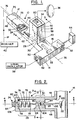
- a mixer 10 is constructed in accordance with the invention, and includes a first waveguide 12, a second waveguide 14 abutting an end of the first waveguide 12 at a first input port 16 of the first waveguide 10, and a third waveguide 18 abutting a side of the first waveguide 12 at a second input port 20 of the first waveguide 12.
- Essential components of the mixer 10 are indicated in phantom view and in cut-away view in Fig. 1, with further details of the components being disclosed in the sectional views of Figs. 2 - 4.
- These components include an input probe 22 in the first input port 16 for coupling microwave power from the second waveguide 14 to the first waveguide 12, a filter 24 located in an output section 26 of the first waveguide 12, and two mixing diodes 28 located in a mixing section 30 of the first waveguide 12 between the probe 22 and the filter 24.
- the probe 22, the diodes 28, and components of the filter 24 (to be disclosed hereinafter) are supported by a plate 32 of dielectric electrically-insulating material disposed parallel to a broad wall of the first waveguide 12 and approximately at a central plane of the first waveguide 12.
- Flanges used in interconnecting the three waveguides 12, 14 and 18 in accordance with well-known construction practice have been deleted for simplicity in portraying the mixer 10. It is understood that other modes of fabrication may be employed such as a brazing together of the waveguides or a molding of the entire assembly of the mixer 10.
- two microwave signals of different frequencies are inputted to the mixer 10 via the second waveguide 14 and the third waveguide 18 to interact in the mixing section 30, via a well-known nonlinear fashion with the diodes 28, to produce signals at other frequencies.
- the signals at the other frequencies include an IF signal wherein the intermediate frequency is typically an order of magnitude less than the frequencies of the inputted microwave signals.
- a further frequency produced by the nonlinear interaction is an image-frequency signal.
- the two inputted microwave signals include an RF input signal and a reference LO input signal.
- the RF input signal has a frequency of 67 GHz (gigahertz), and the reference LO input signal has a frequency of 61 GHz.
- the intermediate frequency has a value of 6 GHz which is equal to the difference between the RF and LO signal frequencies.
- the frequency of the image signal is 55 GHz which is equal to 2(LO) - RF, namely, the difference of twice the LO signal frequency minus the RF signal frequency.
- the filter 24 has a passband centered at the intermediate frequency, 6 GHz, for passing the IF signal from the mixing section 30 to an output port 34 of the first waveguide 12.
- the filter 24 reflects signals at the image signal frequency back to the mixing section 30 for interaction via the diodes 28 with the reference LO signal. Interaction of the reflected image signal with the reference signal produces additional signal at the intermediate frequency in phase with the originally produced IF signal. For example, Interaction of the image signal at 55 GHz with the LO signal at 61 GHz produces a signal at a frequency of 6 GHz which is the difference between the LO signal frequency and the image signal frequency. Thereby, the invention provides for more IF power and improved SNR.
- the third waveguide 18 may be connected to an antenna 36 for receipt of a microwave RF signal, a first end of the second waveguide 14 may be coupled to a local oscillator 38 for receipt of the reference LO signal, and a receiver 40 may be coupled to the output port 34 for receipt of the IF signal.
- a sliding end wall, or shorting wall 42 is disposed in a second end of the second waveguide 14, and is adjusted in position by a positioning mechanism 44 for tuning the second waveguide 14 and its connection to the first input port 16 for maximizing power flow of the LO signal into the mixing section 30.
- each of the waveguides 12, and 14 is fabricated, in a preferred embodiment of the invention, of a metal such as brass or aluminum, and is provided with a rectangular cross-section in which the interior dimension, or width, of a broad wall is twice the interior dimension, or height, of a sidewall.
- the first waveguide 12 has broad walls 46 and sidewalls 48.
- the second waveguide 14 has broad walls 50 and sidewalls 52.
- the third waveguide 18 is constructed of the same material as the other waveguides 12 and 14, and is provided with a cross-section of varying dimensions.
- the third waveguide 18 has a broad wall 54 of constant width, and a sidewall 56 of varying height to provide for a tapered section 58 which acts as an impedance transformer for matching the impedance of an input end 60 of the waveguide 18 to a reduced-height section 62, the reduced height section 62 terminating at the second input port 20.
- the mixing section 30 of the first waveguide 12 has a reduced width defining a channel 64 for matching the impedance of an input section 66 of the first waveguide 12 to the impedance presented by the two mixing diodes 28.
- the width of the channel 64 as measured in a plane parallel to a broad wall 46 of the first waveguide 12 is equal to the height of the reduced height section 62 as measured in a plane parallel to the sidewall 56 of the third waveguide 18.
- the impedance of the mixing diodes 28 is matched to both the channel 64 of the first waveguide 12 and to the reduced-height section 62 of the third waveguide 18.
- the channel 64 in the first waveguide 12 is defined by a pair of abutments 68 extending inwardly from the sidewalls 48.
- the filter 24 comprises a set of three resonators 70, 72, and 74 supported on the plate 32 and located serially along a central axis 76 (Fig. 1) of the first waveguide 12.
- the resonators 70, 72, and 74 are fabricated as metal blocks and are spaced apart from each other and are connected electrically by metallic strips 78.
- Tuning elements 80 and 82 having the form of elongated cylindrical metal slugs are disposed on opposite ends of the series of resonators, the tuning element 80 being connected by a metallic strip 78 to the resonator 70, and the tuning element 82 being connected by a further metallic strip 78 to the resonator 74.
- the metallic strips 78 and the tuning elements 80 and 82 are disposed also along the axis 76.
- the tuning element 82 extends into the output port 34, the output port 34 including a connector 84 to enable connection of a coaxial transmission line (not shown) to the output port 34.
- the connector 84 may be constructed in the customary fashion including an outer metallic shell 86 which surrounds a central metallic conductor 88, and includes an annular dielectric slug 90 disposed between the central conductor 88 and the shell 86.
- the probe 22 comprises a bulb 100 located within the second waveguide 14, and a rod 102 disposed along the axis 76 and extending from the bulb 100 through the input section 66 to connect via a metallic strip 104 with the tuning element 80.
- the metallic strip 104 also connects with a junction of the two diodes 28.
- the tuning elements 80 and 82, the metallic strip 78, and the strip 104 are supported by the plate 32.
- the rod 102 and the bulb 100 of the probe 22 are formed of a metal such as brass or aluminum.
- the configuration of the probe 22, including the rod 102 and the bulb 100 aids in coupling the reference LO signal from the second waveguide 14 into the first waveguide 12 for interaction with the diodes 28.
- the output port 34 is formed as a cylindrical passage in an end wall 106 of the first waveguide 12, the end wall 106 in cooperation with the abutments 68, the broad walls 46 and the sidewalls 48 defining a cavity which encloses the resonators 70, 72, and 74 to aid in establishing the desired characteristics of the filter 24.
- the second waveguide 14 supports a transverse electric (TE) wave
- the third waveguide 18 also supports a TE wave with the electric field, in each of the waveguides 14 and 18, extending perpendicularly to the broad walls.
- the broad walls 50 of the second waveguide 14 are coplanar with the corresponding broad walls 46 of the first waveguide 12.
- the diodes 28 act as detectors of the LO signal and, upon a detection of the LO signal, develop a DC bias voltage.
- the RF input signal is of lower amplitude than the LO signal and interacts with the LO signal in a nonlinear region of the current-voltage characteristic of the diode 28 to produce signals at a plurality of harmonic frequencies including the IF signal and the image signal.
- the mixer 10 has been found to be operative over a bandwidth of 2 GHz for producing the increased output power of IF signal.
- the cross-sectional dimensions of the first waveguide 12 and of the second waveguide 14, for the foregoing frequencies of operation, are 148 mils by 74 mils.
- Each of the diodes 28 has an impedance of 100 ohms, the two diodes 28 being connected in series across the channel 64 to provide a combined impedance of 200 ohms which is presented to the RF and to the LO signals.
- the coplanar and perpendicular relationship between the second waveguide 14 and the first waveguide 12, and the perpendicular relationship of the third waveguide 18 to the common plane of both the first waveguide 12 and the second waveguide 14 provides for an orthogonal relationship of the LO and the RF signals for isolation of these two signals from each other, and from the resulting IF signal.
- the reference LO signal propagates via the second waveguide 14 to the probe 22, whereupon the reference signal is coupled via the probe 22 into the first waveguide 12 and into the mixing section 30 for interaction with the diodes 28.
- the RF signal is inputted via the third waveguide 18 to impinge upon the diodes 28 in the channel 64 to interact with the diodes 28.
- the plate 32 is parallel to the broad walls 46 of the first waveguide 12, and supports the diodes 28 at a position for interaction with both the RF input signal and the reference LO signal to produce the IF signal and an image signal.
- the sizes and spacings of the resonators 70, 72, and 74 are selected in accordance with well known practice to provide a pass band for the IF signal for communicating the IF signal from the mixing section 30 to the output port 34. It is noted that the construction of the microwave circuit including the rod 102, the strip 104, the tuning elements 80 and 82, the strip 78 and the resonators 70, 72, and 74 within the enclosing metallic, electrically-conductive structure of the broad walls 46 and the sidewalls 48 constitute a structure which supports a transverse electromagnetic (TEM) wave. Thus, all frequencies of interest can propagate along the microwave structure in the TEM mode.
- TEM transverse electromagnetic
- the filter 24 is transmissive at a passband centered at the intermediate frequency, and reflects signal at other frequencies, in particular, the image frequency.
- the cross-sectional dimensions of the reduced-height section 62 of the third waveguide 18 provide the characteristics of a waveguide below cutoff frequency for both the IF signal and the image signal. Therefore, other than by propagation in an evanescent mode with severe attenuation, there is essentially no propagation of the IF and the image signals from the mixing section 30 through the third waveguide 18.
- the image signal is substantially trapped in the microwave structure and is reflected back to the diodes 28 for further interaction with the reference LO signal to produce still more signal at the intermediate frequency.
- the microwave structure is tuned to provide a cophasal relationship between the originally produced IF signal and the additional production of signal at the intermediate frequency upon interaction of the image signal with the reference signal.
- the mixer 10 produces significantly more power at the IF signal outputted from the output port 34 with significantly increased signal-to-noise ratio than has been possible heretofore.
Landscapes
- Physics & Mathematics (AREA)
- Electromagnetism (AREA)
- Engineering & Computer Science (AREA)
- Power Engineering (AREA)
- Control Of Motors That Do Not Use Commutators (AREA)
- Radar Systems Or Details Thereof (AREA)
Applications Claiming Priority (2)
| Application Number | Priority Date | Filing Date | Title |
|---|---|---|---|
| US07/692,412 US5265268A (en) | 1991-04-29 | 1991-04-29 | Image recovery mixer |
| US692412 | 1991-04-29 |
Publications (3)
| Publication Number | Publication Date |
|---|---|
| EP0511604A2 true EP0511604A2 (fr) | 1992-11-04 |
| EP0511604A3 EP0511604A3 (en) | 1994-06-08 |
| EP0511604B1 EP0511604B1 (fr) | 1999-05-26 |
Family
ID=24780481
Family Applications (1)
| Application Number | Title | Priority Date | Filing Date |
|---|---|---|---|
| EP92107072A Expired - Lifetime EP0511604B1 (fr) | 1991-04-29 | 1992-04-24 | Mélangeur de reconnaissance d'image |
Country Status (4)
| Country | Link |
|---|---|
| US (1) | US5265268A (fr) |
| EP (1) | EP0511604B1 (fr) |
| CA (1) | CA2064979C (fr) |
| DE (1) | DE69229247T2 (fr) |
Cited By (2)
| Publication number | Priority date | Publication date | Assignee | Title |
|---|---|---|---|---|
| WO2002048735A1 (fr) * | 2000-12-15 | 2002-06-20 | Thales | Radar large bande et modulateur, notamment pour commuter des ondes hyperfrequence sur une tres courte duree |
| CN106207346A (zh) * | 2016-07-27 | 2016-12-07 | 中国电子科技集团公司第四十研究所 | 一种低本振功率的宽中频毫米波基波混频电路 |
Families Citing this family (4)
| Publication number | Priority date | Publication date | Assignee | Title |
|---|---|---|---|---|
| US5765100A (en) * | 1995-02-03 | 1998-06-09 | Symbol Technologies, Inc. | Communication diversity by image reception |
| US6427069B1 (en) * | 2000-05-12 | 2002-07-30 | Israel Galin | Balanced all-wavelength sub-millimeter microwave subharmonic mixer |
| JP4134226B2 (ja) * | 2004-03-10 | 2008-08-20 | 東京エレクトロン株式会社 | 分配器および方法、プラズマ処理装置および方法、並びに、lcdの製造方法 |
| CN108054480B (zh) * | 2017-12-11 | 2019-06-07 | 合肥中科离子医学技术装备有限公司 | 一种用于发射机的多路功率合成装置 |
Family Cites Families (6)
| Publication number | Priority date | Publication date | Assignee | Title |
|---|---|---|---|---|
| US3562651A (en) * | 1968-05-27 | 1971-02-09 | Watkins Johnson Co | Microwave hybrid junction circuit and frequency translators constructed therefrom |
| US3681697A (en) * | 1969-12-31 | 1972-08-01 | Westinghouse Electric Corp | Wideband image terminated mixer |
| NL7704644A (nl) * | 1977-04-28 | 1978-10-31 | Hollandse Signaalapparaten Bv | Mengelement. |
| US4291415A (en) * | 1979-12-03 | 1981-09-22 | Microwave Associates, Inc. | Microwave integrated circuit double balanced mixer |
| IT1155664B (it) * | 1982-03-25 | 1987-01-28 | Sip | Dispositivo di guida d onda per la separazione di segnali a radiofrequenza di diversa frequenza e polarizzazione |
| US4654887A (en) * | 1985-11-04 | 1987-03-31 | Raytheon Company | Radio frequency mixer |
-
1991
- 1991-04-29 US US07/692,412 patent/US5265268A/en not_active Expired - Lifetime
-
1992
- 1992-04-02 CA CA002064979A patent/CA2064979C/fr not_active Expired - Fee Related
- 1992-04-24 EP EP92107072A patent/EP0511604B1/fr not_active Expired - Lifetime
- 1992-04-24 DE DE69229247T patent/DE69229247T2/de not_active Expired - Fee Related
Cited By (3)
| Publication number | Priority date | Publication date | Assignee | Title |
|---|---|---|---|---|
| WO2002048735A1 (fr) * | 2000-12-15 | 2002-06-20 | Thales | Radar large bande et modulateur, notamment pour commuter des ondes hyperfrequence sur une tres courte duree |
| FR2818385A1 (fr) * | 2000-12-15 | 2002-06-21 | Thomson Csf | Radar large bande et modulateur, notamment pour commuter des ondes hyperfrequence sur une tres courte duree |
| CN106207346A (zh) * | 2016-07-27 | 2016-12-07 | 中国电子科技集团公司第四十研究所 | 一种低本振功率的宽中频毫米波基波混频电路 |
Also Published As
| Publication number | Publication date |
|---|---|
| EP0511604A3 (en) | 1994-06-08 |
| DE69229247D1 (de) | 1999-07-01 |
| DE69229247T2 (de) | 1999-09-23 |
| CA2064979C (fr) | 1997-03-25 |
| EP0511604B1 (fr) | 1999-05-26 |
| US5265268A (en) | 1993-11-23 |
| CA2064979A1 (fr) | 1992-10-30 |
Similar Documents
| Publication | Publication Date | Title |
|---|---|---|
| US5142255A (en) | Planar active endfire radiating elements and coplanar waveguide filters with wide electronic tuning bandwidth | |
| US4596047A (en) | Satellite broadcasting receiver including a parabolic antenna with a feed waveguide having a microstrip down converter circuit | |
| US4371853A (en) | Strip-line resonator and a band pass filter having the same | |
| US3369197A (en) | Waveguide mode coupler | |
| US4418429A (en) | Mixer for use in a microwave system | |
| US4641369A (en) | Local oscillator and mixer assembly | |
| US5265268A (en) | Image recovery mixer | |
| US4168478A (en) | Apparatus for separating electrical signals of different frequencies | |
| JPH08191204A (ja) | リッジ導波管空洞フィルタ | |
| EP0906657B1 (fr) | Convertisseur de frequences pour des applications a des ondes radioelectriques millimetriques | |
| US4270224A (en) | Microwave down converter | |
| US5471177A (en) | Octave band gap diplexer | |
| US2813972A (en) | Microwave mixer | |
| US4752753A (en) | Coaxial waveguide band reject filter | |
| US4427953A (en) | Microwave diplexer | |
| EP0961339B1 (fr) | Dispositif d'émission/réception de signaux | |
| US4458217A (en) | Slot-coupled microwave diplexer and coupler therefor | |
| Lehto et al. | Embedding impedance of a millimeter wave Schottky mixer: scaled model measurements and computer simulations | |
| Frerking et al. | A broad-band low-noise 205 GHz radiometer for a satellite receiver | |
| CA1203578A (fr) | Melangeur pour utilisation dans un systeme micro- ondes | |
| US12548872B2 (en) | Balanced bandpass filters for millimeter-wave applications | |
| US6389274B1 (en) | Subharmonic frequency converter for applications to millimetric radio waves | |
| KR100358978B1 (ko) | Nrd 가이드용 주파수 변환기 | |
| Ho et al. | High performance MM-wave balanced mixers for Ka band down converters | |
| JPH0213961B2 (fr) |
Legal Events
| Date | Code | Title | Description |
|---|---|---|---|
| PUAI | Public reference made under article 153(3) epc to a published international application that has entered the european phase |
Free format text: ORIGINAL CODE: 0009012 |
|
| 17P | Request for examination filed |
Effective date: 19920424 |
|
| AK | Designated contracting states |
Kind code of ref document: A2 Designated state(s): DE FR GB IT |
|
| PUAL | Search report despatched |
Free format text: ORIGINAL CODE: 0009013 |
|
| AK | Designated contracting states |
Kind code of ref document: A3 Designated state(s): DE FR GB IT |
|
| 17Q | First examination report despatched |
Effective date: 19961024 |
|
| GRAG | Despatch of communication of intention to grant |
Free format text: ORIGINAL CODE: EPIDOS AGRA |
|
| RAP1 | Party data changed (applicant data changed or rights of an application transferred) |
Owner name: HE HOLDINGS, INC. |
|
| RAP1 | Party data changed (applicant data changed or rights of an application transferred) |
Owner name: HUGHES ELECTRONICS CORPORATION |
|
| GRAG | Despatch of communication of intention to grant |
Free format text: ORIGINAL CODE: EPIDOS AGRA |
|
| GRAH | Despatch of communication of intention to grant a patent |
Free format text: ORIGINAL CODE: EPIDOS IGRA |
|
| GRAH | Despatch of communication of intention to grant a patent |
Free format text: ORIGINAL CODE: EPIDOS IGRA |
|
| GRAA | (expected) grant |
Free format text: ORIGINAL CODE: 0009210 |
|
| AK | Designated contracting states |
Kind code of ref document: B1 Designated state(s): DE FR GB IT |
|
| REF | Corresponds to: |
Ref document number: 69229247 Country of ref document: DE Date of ref document: 19990701 |
|
| ET | Fr: translation filed | ||
| PLBE | No opposition filed within time limit |
Free format text: ORIGINAL CODE: 0009261 |
|
| STAA | Information on the status of an ep patent application or granted ep patent |
Free format text: STATUS: NO OPPOSITION FILED WITHIN TIME LIMIT |
|
| 26N | No opposition filed | ||
| REG | Reference to a national code |
Ref country code: GB Ref legal event code: IF02 |
|
| PGFP | Annual fee paid to national office [announced via postgrant information from national office to epo] |
Ref country code: DE Payment date: 20080602 Year of fee payment: 17 |
|
| PGFP | Annual fee paid to national office [announced via postgrant information from national office to epo] |
Ref country code: IT Payment date: 20080429 Year of fee payment: 17 |
|
| PGFP | Annual fee paid to national office [announced via postgrant information from national office to epo] |
Ref country code: FR Payment date: 20080417 Year of fee payment: 17 |
|
| PGFP | Annual fee paid to national office [announced via postgrant information from national office to epo] |
Ref country code: GB Payment date: 20080429 Year of fee payment: 17 |
|
| GBPC | Gb: european patent ceased through non-payment of renewal fee |
Effective date: 20090424 |
|
| REG | Reference to a national code |
Ref country code: FR Ref legal event code: ST Effective date: 20091231 |
|
| PG25 | Lapsed in a contracting state [announced via postgrant information from national office to epo] |
Ref country code: DE Free format text: LAPSE BECAUSE OF NON-PAYMENT OF DUE FEES Effective date: 20091103 |
|
| PG25 | Lapsed in a contracting state [announced via postgrant information from national office to epo] |
Ref country code: GB Free format text: LAPSE BECAUSE OF NON-PAYMENT OF DUE FEES Effective date: 20090424 Ref country code: FR Free format text: LAPSE BECAUSE OF NON-PAYMENT OF DUE FEES Effective date: 20091222 |
|
| PG25 | Lapsed in a contracting state [announced via postgrant information from national office to epo] |
Ref country code: IT Free format text: LAPSE BECAUSE OF NON-PAYMENT OF DUE FEES Effective date: 20090424 |