EP0511711A2 - Circuit logique combinatoire programmable - Google Patents
Circuit logique combinatoire programmable Download PDFInfo
- Publication number
- EP0511711A2 EP0511711A2 EP92201158A EP92201158A EP0511711A2 EP 0511711 A2 EP0511711 A2 EP 0511711A2 EP 92201158 A EP92201158 A EP 92201158A EP 92201158 A EP92201158 A EP 92201158A EP 0511711 A2 EP0511711 A2 EP 0511711A2
- Authority
- EP
- European Patent Office
- Prior art keywords
- gating
- logic
- programming
- switches
- level
- Prior art date
- Legal status (The legal status is an assumption and is not a legal conclusion. Google has not performed a legal analysis and makes no representation as to the accuracy of the status listed.)
- Withdrawn
Links
Images


Classifications
-
- H—ELECTRICITY
- H03—ELECTRONIC CIRCUITRY
- H03K—PULSE TECHNIQUE
- H03K19/00—Logic circuits, i.e. having at least two inputs acting on one output; Inverting circuits
- H03K19/02—Logic circuits, i.e. having at least two inputs acting on one output; Inverting circuits using specified components
- H03K19/173—Logic circuits, i.e. having at least two inputs acting on one output; Inverting circuits using specified components using elementary logic circuits as components
- H03K19/1733—Controllable logic circuits
- H03K19/1738—Controllable logic circuits using cascode switch logic [CSL] or cascode emitter coupled logic [CECL]
-
- H—ELECTRICITY
- H03—ELECTRONIC CIRCUITRY
- H03K—PULSE TECHNIQUE
- H03K17/00—Electronic switching or gating, i.e. not by contact-making and –breaking
- H03K17/51—Electronic switching or gating, i.e. not by contact-making and –breaking characterised by the components used
- H03K17/56—Electronic switching or gating, i.e. not by contact-making and –breaking characterised by the components used by the use, as active elements, of semiconductor devices
- H03K17/687—Electronic switching or gating, i.e. not by contact-making and –breaking characterised by the components used by the use, as active elements, of semiconductor devices the devices being field-effect transistors
- H03K17/693—Switching arrangements with several input- or output-terminals, e.g. multiplexers, distributors
Definitions
- the present invention relates to semiconductor combinational logic circuits such as are employed in programmable logic devices (PLDs), and particularly to such a logic circuit which is programmable to provide any selected combinational logic function of a plurality of logic signals.
- PLDs programmable logic devices
- a programmable logic device is a integrated circuit having a large number of gates which can be programmably interconnected so as to provide a selected logic function. Such devices are available in bipolar, MOS and CMOS technologies, bipolar providing higher speed and MOS (particularly CMOS) having the advantage of lower power consumption. User programmability to establish the appropriate interconnections for a selected logic function may be achieved, for example, by supplying address signals to such interconnections which serves to open fusible links or establish charges on the gates of MOS or CMOS devices. Further description of PLDs can be found, for example, in U.S. Patent No. 4,442,072, issued December 20, 1988, U.S. Patent No.
- the invention provides a programmable logic circuit which is capable of providing any selected combinational logic function of a plurality of input logic signals, a particular logic function being established by programming signals supplied to the circuit, and which can be realized in Bi CMOS technology so as to achieve both high speed operation and relatively low power consumption.
- Logic signal processing may be performed by bipolar transistors operating at small swings in voltage level, at or below those employed in ECL, while the programming signals are supplied to MOS or CMOS transistors requiring zero stand-by power and operating at rail-to-rail swings of such signals. Saturation of the bipolar transistors can be prevented, thereby improving switching speed, by including level shifters at the inputs or outputs of the logic circuit.
- the circuit can also be realized entirely in CMOS technology if somewhat lower operating speed is acceptable.
- a programmable logic circuit in accordance with the invention comprises a tree structure of successive serially connected gating levels, each level being for a respective input logic signal and having one or more pairs of logic switches.
- Each such gating level switch has at least one control terminal, a first current terminal and a second current terminal, the input logic signal for a given gating level being supplied, in complemented or non-complemented form, to the control terminals of the gating switches in that level.
- the gating switches in each pair are thereby alternatively conductive or non-conductive depending on the logic value, i.e. high or low, of the logic signal supplied thereto.
- each gating switch in a given gating level is coupled in common to the first current terminals of both of a pair of gating switches in the next higher gating level, so that each successive gating level has twice as may pairs of gating switches as the preceding level.
- the logic circuit also includes a programming level made up of a plurality of pairs of logic switches, each programming switch having a control terminal and a first and second current terminal, each pair of programming switches receiving a respective programming signal in complemented or non-complemented form at the control terminals thereof, both of the first current terminals of each such pair of switches being coupled to the second current terminal of a respective gating switch in the highest gating level of the circuit.
- the programming switches are thereby controlled by the programming signals so that those in each pair are alternatively conductive or non-conductive depending on the logic value, i.e. high or low, of the relevant programming signal.
- the logic circuit also has an output terminal at which, depending on the logic values of the respective programming signals, the programming switches will produce a logic signal which constitutes a selected logical combination of the input logic signals to the circuit.
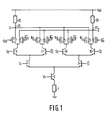
- a logic circuit in accordance with the invention which is programmable to provide any selected combinational logic function of a plurality, in this case two, logic signals S 1 and S 2 .
- the resulting output signal Q, and preferably also its complement Q, are produced at respective output terminals of the circuit.
- Each gating level includes one or more pairs of logic switches, which in the embodiment in Fig. 1 are in the form of NPN bipolar transistors which each have a control terminal, a first current terminal, and a second current terminal. More specifically, the control terminal is at the base and the first and second current terminals are respectively at the emitter and collector. It will be obvious that with appropriate changes of polarity of the various signals and power supply voltages PNP transistors could equally well be employed.
- the first logic signal S 1 and its complement"S 1 are respectively supplied to the control terminals, i.e. the bases of a pair of transistors 1 and 3 in the first gating level of the circuit.
- the control terminals i.e. the bases of a pair of transistors 1 and 3 in the first gating level of the circuit.
- the emitters of transistors 1 and 3 are connected in common to a constant current source which may conveniently be an NPN transistor 5 in series with a resistor 7 which is connected to ground, the base of transistor 5 being supplied with a constant bias voltage Vb which results in adequate collector current so that the transistors 1,3, 9, 11, 13 and 15 of the gating levels all operate at current levels appropriate for their dimensions and consequently at their optimum switching speed.
- a constant current source which may conveniently be an NPN transistor 5 in series with a resistor 7 which is connected to ground, the base of transistor 5 being supplied with a constant bias voltage Vb which results in adequate collector current so that the transistors 1,3, 9, 11, 13 and 15 of the gating levels all operate at current levels appropriate for their dimensions and consequently at their optimum switching speed.
- the second gating level of the circuit in Fig. 1 receives the second logic signal S 2 and comprises two pairs of bipolar NPN transistors; a first pair 9 and 11 the emitters of which are connected in common to the collector of transistor 1 in the first gating level, and a second pair 13 and 15 the emitters of which are connected in common to the collector of transistor 3 in the first gating level.
- the second input signal S 2 and its complement S2 are respectively supplied to the bases of transistors 9 and 11 in the first pair and also to the bases of transistors 13 and 15 in the second pair.
- the second current terminal, i.e., the collector, of each logic switch in the first gating level is coupled in common to both of the first current terminals, i.e.
- the logic circuit would then include a third gating level including four pairs of logic switches, each pair having two bipolar transistors, the two emitters thereof being connected in common to the collector of a respective one of the four transistors 9, 11,13 and 15 in the second gating level.
- the logic circuit has the form of a branching tree structure of successive serially interconnected gating levels, each level being for a respective input logic signal.
- gating levels each level being for a respective input logic signal.
- the input signals at the control terminals of the relevant transistors 3, 11 and 15 can be set at fixed values, for example at about 2.5 volt, with one Vbe difference between the voltages at the different gating levels.
- the logic signals S 1 and S 2 would then need to have a larger voltage swing, for example, from 1.5 to 3.5 volt.
- Programming of the logic circuit is provided by a programming level thereof which is coupled to the highest gating level and includes respective pairs of logic switches for the respective logic switches in the highest gating level.
- Each pair of logic switches in the programming level has at least one control terminal for receiving a logic programming signal, a first current terminal which is coupled to the collector of a respective transistor in the highest gating level, and a pair of second current terminals which are separately coupled to a supply voltage line Vdd via resistors 35 and 39, respectively.
- logic switches in the gating levels will be referred to herein as gating switches and logic switches in the programming level will be referred to herein a programming switches.
- gating switches logic switches in the programming level
- each such pair of programming switches consists of a pair of P channel MOS transistors, the drains thereof being connected together to constitute the aforesaid first current terminal which is connected to the collector of a transistor in a gating switch in the highest gating level.
- a first pair of P channel MOS transistors 17 and 19 have their drains connected together and to the collector of bipolar transistor 9 in the second gating level; a second pair of P channel MOS transistors 21 and 23 have their drains connected together and to the collector of bipolar transistor 11 in the second gating level; a third pair of P channel MOS transistors 25 and 27 have their drains connected together and to the collector of transistor 13 in the second gating levels; and a fourth pair of P channel MOS transistors 29 and 31 have their drains connected together and to the collector of transistor 15 in the second gating level.
- the sources of each of the aforesaid pairs of MOS transistors constitute the above-referred to pair of second current terminals of each such pair.
- a first programming signal g oo and its complement go o are respectively applied to the gates of the first pair of programming switch MOS transistors 17 and 19, a second programming signal go and its complement 901 are respectively applied to the gates of the second pair of programming switch MOS transistors 21 and 23, a third programming signal g io and its complement 910 are respectively applied to the gates of the third pair of programming switch MOS transistors 25 ad 27, ad a fourth programming signal g11 and its complement g 11 are respectively applied to the gates of the fourth pair of programming switch MOS transistors 29 and 31.
- the sources of those of the MOS transistors which receive non-complemented programming signals at their gates are all connected in common to a junction point 33 which is coupled via a path including a resistor 35 to the positive voltage supply rail Vdd.
- the output signal Q of the logic circuit is thereby available at junction point 33.
- the sources of those of the programming switch MOS transistors which receive complemented programming signals at their gates are all connected in common to a junction point 37 which is coupled via a path including a resistor 39 to the positive voltage supply rail Vdd, and a complemented output signal Q of the logic circuit is available at junction point 37.
- Fig. 2 is a modified form of the circuit of Fig. 1 which further enhances the speed of operation.
- the layout and operation of the circuit is largely identical to that in Fig. 1, corresponding elements thereof having the same identifying numerals.
- the improvement over the circuit of Fig. 1 is that a bipolar transistor 41 is included in cascode connection between junction 33 ad resistor 35, and similarly a bipolar transistor 43 is connected in cascode connection between junction point 37 and resistor 39. More specifically, the emitter of transistor 41 is connected to junction point 33 and the collector thereof is connected to resistor 35, and the emitter of transistor 43 is connected to junction point 37 and the collector thereof is connected to resistor 39.
- the bases of transistors 41 and 43 are connected to a source of constant dc reference voltage V" and the output signals Q and Q of the logic circuit are respectively produced at the collectors of transistors 41 and 43.
- Such cascode connections are well known, and serve to compensate for the collector- base feedback capacitances of the the bipolar transistors in the logic circuit.
- a constant current source formed by the transistor 5 and the resistor 7, further avoids saturation effects in the layer of transistors connected closest to the voltage supply line Vdd, whether these are the programming switches 17 to 31 as in Fig. 1, or the cascode transistors 41 and 43 as in Fig. 2.
- the programming signals for implementing a selected combinational logic function of the input signals S 1 and S 2 may typically be obtained from a CMOS static memory wherein such signals are stored at respective addresses. Consequently, the programming signals will be enumerated herein as if they were binary addresses in such a memory. It will be noted that with (L) logic signals there will be (L) gating levels, any nth gating level having 2 n logic switches and so 2 n control terminals. Consequently, to cover all possible combinational logic functions 2 L programming signals will be required. That can be achieved, as shown in Fig. 1, by providing 2 L programming signals along with the complements thereof.
- CMOS-logic complementary MOS transistors
- transistor 1 in the first gating level and transistor 9 coupled thereto in the second gating level will both be in the conductive or "on” state.
- Transistors 3 and 11 will be “off”. As transistor 3 is “off”, the state of transistors 13 and 15, “on” and “off” respectively, does not matter.
- the programming signal g oo is high, its complement goo will be low and so in the programming level MOS transistor 17 will be non-conductive or "off” and MOS transistor 19 will be conductive or "on”.
- a NOR operation will be obtained at the Q output, as seen from equation (1), when the only non-complemented programming signal which is high is g 11 .
- the logic circuit of Fig. 1 can be employed as a prototype for a final version thereof to be included in a complete PLD, since it can be easily programmed and reprogrammed, even during operation, while debugging of the complete device is carried out. Eprom transistors or possibly fusible links can then be substituted for the programming switches. This mode of design makes it possible to significantly reduce the production cost of the final device.
- the dc level of the input logic signals S 1 and S 2 should be within predetermined limits. That can be achieved by providing a level shifter for each of the input logic signals and using the outputs of such level shifters as the actual logic signals which are input to the gating circuit.
- level shifters are well known, one example being shown in Fig. 3. Therein there are two diode- connected bipolar transistors in series between a bipolar transistor 45, the collector of which is connected to Vdd, and a current level setting bipolar transistor 47 which is supplied with a fixed base bias voltage Vb. The emitter of transistor 47 is returned to ground by a resistor 49. The input logic signal Vin is supplied to the base transistor 45.
- the corresponding output signal can be taken at the emitter of any of such transistors, except the current source transistor 47, and will be equal to Vin less a number of base-emitter voltage drops Vbe equal to the number of transistors up to and including that at which the output is taken.
- CMOS complementary metal-oxide-semiconductor
- Fig. 4 This embodiment of the invention is shown in Fig. 4.
- the CMOS logic circuit in Fig. 4 has respective gating levels for the respective input logic signals.
- the first gating level has one pair of switches 54 and 58 for receiving logic signal S 1 and its complement - 91 .
- Each of such switches has a pair of current terminals, a first control terminal which receives the signal Si, and a second control terminal which receives the complement signal S 1 .
- the second gating level has two pairs of such logic switches, the first current terminals of each such pair being connected together and to the second current terminal of one of the logic switches in the first gating level.
- the first control terminals of each such pair receive the input logic signal S 2
- the second control terminals of each such pair receive the complement logic signal S 2 .
- each logic switch consists of a pair of CMOS transistors connected in parallel, the sources thereof being connected together to constitute a first current terminal and the drains thereof being connected together to constitute a second current terminal, thereby forming two oppositely directed transmission paths, one direction for producing the non-complemented Q output signal of the gate circuit and the other direction for producing the complemented Q output signal.
- the logic switch 54 includes P channel MOS transistor 51 and N channel MOS transistor 53
- the logic switch 58 includes P channel MOS transistor 55 and N channel MOS transistor 57.
- the common drain connections of both of such switches are connected to an output terminal 59, at which the Q output signal of the logic circuit is produced.
- An inverter 60 coupled to terminal 59 provides the non-complemented output signal Q.
- the second gating level of the logic circuit in Fig. 3 comprises two pairs of logic switches, one pair being switches 60 and 61 and the other being switches 62 and 63, each of such switches being of the same construction as switches 54 and 58 in the first gating level.
- the common drain connections of the switch pairs 60 and 61 are both being connected to the common source connection of CMOS transistors 51 and 53 of logic switch 54 in the first gating level, the latter connection constituting the second current terminal of logic switch 54.
- the common drain connections of the switch pair 62 and 63 are both connected to the common source connection of CMOS transistors 55 and 57 of logic switch 58 in the third gating level, the latter connection constituting the second current terminal of logic switch 58.
- the common source connections of the respective logic switches 60, 61, 62 and 63, which constitute the second current terminals thereof, are respectively connected to the first current terminals of the respective CMOS gates 64, 65, 66 and 67 which comprise the programming level of the logic circuit.
- Each of the latter switches is of the same construction as CMOS switches 54 and 58 in the first gating level.
- the source of the P channel MOS transistor is connected to the Vdd positive supply rail and the source of the N channel MOS transistor is connected to ground.
- the four CMOS logic switches 64, 65, 66 and 67 respectively receive respective programming signal goo, go,, g10 and g 11 , each programming signal being supplied to the gates of both of the MOS transistors in the relevant logic switch.
- the first logic input signal S1 which controls the first gating level, is supplied to the gate of N channel transistor 53 in logic gate 54 and also to the gate of P channel transistor 55 in logic gate 58.
- the complement"S 1 of such input signal is supplied to the gates of the remaining complementary transistors 51 and 57 in logic gates 54 and 58, respectively.
- the second logic input signal S2, which controls the second gating level is supplied to the gates of the N and P channel transistors in logic switches 60 and 61, respectively; and also to the gates of the N and P channel transistors in logic switches 62 and 63, respectively.
- the complement S 2 of such input signal is supplied to the gates of the remaining complementary transistors in each of logic gates 60, 61, 62 and 63.
- an N channel transistor of a logic switch in the gating level will conduct in response to a "1" " logic signal at the gate thereof if its source is at the "O” signal level
- the P channel transistor of such logic switch will conduct in response to a "O” logic signal at the gate thereof if its source is at the "1” signal level.
- the goo programming signal for example, if it is a "1” it it will turn on the N channel transistor in programming switch 64, and since the source of such transistor is connected to ground a “O” will be produced at the drain thereof. Such “O” is thereby supplied to the second current terminal of switch 60 in the second gating level, and thus to the sources of the transistors therein. If the input signal S2 is "1", the N channel transistor in switch 60 will therefore conduct and produce a "O” at the drain thereof and so at the first current terminal of switch 60. A “O” is thereby applied to the second current terminal of logic switch 54 in the first gating level.
- MOS transistor signifies any type of insulated gate field effect transistor, and not necessarily one in which the gate is a metal on oxide arrangement.
- MOS transistor signifies any type of insulated gate field effect transistor, and not necessarily one in which the gate is a metal on oxide arrangement.
Landscapes
- Physics & Mathematics (AREA)
- Engineering & Computer Science (AREA)
- Computer Hardware Design (AREA)
- Computing Systems (AREA)
- General Engineering & Computer Science (AREA)
- Mathematical Physics (AREA)
- Logic Circuits (AREA)
Applications Claiming Priority (2)
| Application Number | Priority Date | Filing Date | Title |
|---|---|---|---|
| US695036 | 1991-05-01 | ||
| US07/695,036 US5124588A (en) | 1991-05-01 | 1991-05-01 | Programmable combinational logic circuit |
Publications (2)
| Publication Number | Publication Date |
|---|---|
| EP0511711A2 true EP0511711A2 (fr) | 1992-11-04 |
| EP0511711A3 EP0511711A3 (en) | 1995-03-15 |
Family
ID=24791289
Family Applications (1)
| Application Number | Title | Priority Date | Filing Date |
|---|---|---|---|
| EP92201158A Withdrawn EP0511711A3 (en) | 1991-05-01 | 1992-04-24 | Programmable combinational logic circuit |
Country Status (3)
| Country | Link |
|---|---|
| US (1) | US5124588A (fr) |
| EP (1) | EP0511711A3 (fr) |
| JP (1) | JPH05145405A (fr) |
Cited By (2)
| Publication number | Priority date | Publication date | Assignee | Title |
|---|---|---|---|---|
| EP0898370A1 (fr) * | 1997-08-19 | 1999-02-24 | Hewlett-Packard Company | Famille logique CMOS différentielle |
| FR2792475A1 (fr) * | 1999-04-16 | 2000-10-20 | St Microelectronics Sa | Comparateur d'une valeur numerique ayant des niveaux de tension cmos et d'une valeur numerique ayant des niveaux de tension ecl |
Families Citing this family (13)
| Publication number | Priority date | Publication date | Assignee | Title |
|---|---|---|---|---|
| US5686791A (en) | 1992-03-16 | 1997-11-11 | Microelectronics And Computer Technology Corp. | Amorphic diamond film flat field emission cathode |
| FR2724073A1 (fr) * | 1994-08-31 | 1996-03-01 | Sgs Thomson Microelectronics | Circuit logique a etages differentiels |
| JP2728013B2 (ja) * | 1995-03-10 | 1998-03-18 | 日本電気株式会社 | BiCMOS論理ゲート回路 |
| WO1997047088A1 (fr) * | 1996-06-04 | 1997-12-11 | Hitachi, Ltd. | Circuit integre a semi-conducteur |
| GB2318664B (en) | 1996-10-28 | 2000-08-23 | Altera Corp | Embedded logic analyzer for a programmable logic device |
| US6286114B1 (en) * | 1997-10-27 | 2001-09-04 | Altera Corporation | Enhanced embedded logic analyzer |
| US6408501B1 (en) | 1998-07-30 | 2002-06-25 | Central Corporation | Automatic system of manufacturing ball studs for vehicles |
| US6754862B1 (en) | 2000-03-09 | 2004-06-22 | Altera Corporation | Gaining access to internal nodes in a PLD |
| US7036046B2 (en) * | 2002-11-14 | 2006-04-25 | Altera Corporation | PLD debugging hub |
| US7076751B1 (en) | 2003-01-24 | 2006-07-11 | Altera Corporation | Chip debugging using incremental recompilation |
| US7539900B1 (en) | 2003-07-29 | 2009-05-26 | Altera Corporation | Embedded microprocessor for integrated circuit testing and debugging |
| US7206967B1 (en) | 2004-02-09 | 2007-04-17 | Altera Corporation | Chip debugging using incremental recompilation and register insertion |
| US8296604B1 (en) * | 2009-10-12 | 2012-10-23 | Xilinx, Inc. | Method of and circuit for providing temporal redundancy for a hardware circuit |
Family Cites Families (14)
| Publication number | Priority date | Publication date | Assignee | Title |
|---|---|---|---|---|
| US3691401A (en) * | 1971-03-10 | 1972-09-12 | Honeywell Inf Systems | Convertible nand/nor gate |
| JPS5244551A (en) * | 1975-10-06 | 1977-04-07 | Toshiba Corp | Logic circuit |
| JPS59208943A (ja) * | 1983-05-12 | 1984-11-27 | Matsushita Electric Ind Co Ltd | 論理回路 |
| JPS6018892A (ja) * | 1983-07-12 | 1985-01-30 | Sharp Corp | 半導体デコ−ダ回路 |
| KR920011006B1 (ko) * | 1983-08-22 | 1992-12-26 | 가부시끼가이샤 히다찌세이사꾸쇼 | 반도체 집적회로 장치 |
| GB8324710D0 (en) * | 1983-09-15 | 1983-10-19 | Ferranti Plc | Bipolar transistor logic circuits |
| JPS60113525A (ja) * | 1983-11-24 | 1985-06-20 | Sharp Corp | Eclゲ−ト回路 |
| JPS6165623A (ja) * | 1984-09-07 | 1986-04-04 | Nippon Telegr & Teleph Corp <Ntt> | Cmosセレクタ回路 |
| US4620117A (en) * | 1985-01-04 | 1986-10-28 | Advanced Micro Devices, Inc. | Balanced CMOS logic circuits |
| FR2581811A1 (fr) * | 1985-05-10 | 1986-11-14 | Radiotechnique Compelec | Module multiplexeur numerique a n entrees et multiplexeur a n2 entrees incorporant de tels modules |
| US4754173A (en) * | 1985-06-13 | 1988-06-28 | Digital Equipment Corporation | Emitter coupled logic latch with boolean logic input gating network |
| US4713560A (en) * | 1986-06-05 | 1987-12-15 | Fairchild Semiconductor Corporation | Switched impedance emitter coupled logic gate |
| US4963767A (en) * | 1988-08-25 | 1990-10-16 | National Semiconductor Corporation | Two-level ECL multiplexer without emitter dotting |
| DE3883389T2 (de) * | 1988-10-28 | 1994-03-17 | Ibm | Zweistufige Adressendekodierschaltung für Halbleiterspeicher. |
-
1991
- 1991-05-01 US US07/695,036 patent/US5124588A/en not_active Expired - Fee Related
-
1992
- 1992-04-24 EP EP92201158A patent/EP0511711A3/en not_active Withdrawn
- 1992-04-30 JP JP4111769A patent/JPH05145405A/ja active Pending
Cited By (4)
| Publication number | Priority date | Publication date | Assignee | Title |
|---|---|---|---|---|
| EP0898370A1 (fr) * | 1997-08-19 | 1999-02-24 | Hewlett-Packard Company | Famille logique CMOS différentielle |
| US6008670A (en) * | 1997-08-19 | 1999-12-28 | Hewlett-Packard | Differential CMOS logic family |
| FR2792475A1 (fr) * | 1999-04-16 | 2000-10-20 | St Microelectronics Sa | Comparateur d'une valeur numerique ayant des niveaux de tension cmos et d'une valeur numerique ayant des niveaux de tension ecl |
| US6335677B1 (en) | 1999-04-16 | 2002-01-01 | Stmicroelectronics S.A. | Comparator of a digital value having CMOS voltage levels with a digital value having ECL voltage levels |
Also Published As
| Publication number | Publication date |
|---|---|
| EP0511711A3 (en) | 1995-03-15 |
| US5124588A (en) | 1992-06-23 |
| JPH05145405A (ja) | 1993-06-11 |
Similar Documents
| Publication | Publication Date | Title |
|---|---|---|
| US5124588A (en) | Programmable combinational logic circuit | |
| US7046041B1 (en) | Structures and methods of implementing a pass gate multiplexer with pseudo-differential input signals | |
| US4575648A (en) | Complementary field effect transistor EXCLUSIVE OR logic gates | |
| KR900003070B1 (ko) | 논리회로 | |
| US4041326A (en) | High speed complementary output exclusive OR/NOR circuit | |
| US3551693A (en) | Clock logic circuits | |
| JPH06169252A (ja) | プログラム可能な論理回路装置 | |
| US4408134A (en) | Unitary exclusive or-and logic circuit | |
| US4091293A (en) | Majority decision logic circuit | |
| EP0085569A2 (fr) | Circuit logique à l'arséniure de gallium | |
| US5909187A (en) | Current steering circuit for a digital-to-analog converter | |
| KR890015425A (ko) | 바이폴라 트랜지스터와 cmos 트랜지스터를 사용한 반도체 집적회로 | |
| US3660678A (en) | Basic ternary logic circuits | |
| US5664211A (en) | Null convention threshold gate | |
| KR930004351B1 (ko) | 레벨 변환회로 | |
| US4943740A (en) | Ultra fast logic | |
| US4801819A (en) | Clocked CMOS circuit with at least one CMOS switch | |
| US4717845A (en) | TTL compatible CMOS input circuit | |
| US3430071A (en) | Logic circuit | |
| USRE35483E (en) | Switching matrix crosspoint | |
| US5198704A (en) | Bi-CMOS output circuit with limited output voltage | |
| US6255857B1 (en) | Signal level shifting circuits | |
| US6072413A (en) | Current output type digital-to-analog converter capable of suppressing output current fluctuation using a current mirror | |
| US4977338A (en) | High speed bipolar-MOS logic circuit including a series coupled arrangement of a bipolar transistor and a logic block having a MOSFET | |
| US4845387A (en) | Non-stacked ECL type and function |
Legal Events
| Date | Code | Title | Description |
|---|---|---|---|
| PUAI | Public reference made under article 153(3) epc to a published international application that has entered the european phase |
Free format text: ORIGINAL CODE: 0009012 |
|
| AK | Designated contracting states |
Kind code of ref document: A2 Designated state(s): DE FR GB IT |
|
| PUAL | Search report despatched |
Free format text: ORIGINAL CODE: 0009013 |
|
| AK | Designated contracting states |
Kind code of ref document: A3 Designated state(s): DE FR GB IT |
|
| 17P | Request for examination filed |
Effective date: 19950915 |
|
| STAA | Information on the status of an ep patent application or granted ep patent |
Free format text: STATUS: THE APPLICATION HAS BEEN WITHDRAWN |
|
| 18W | Application withdrawn |
Withdrawal date: 19960409 |