EP0512679A2 - Méthode de fabrication de films orientés par ablation par laser sur substrats métalliques et articles ainsi obtenus - Google Patents
Méthode de fabrication de films orientés par ablation par laser sur substrats métalliques et articles ainsi obtenus Download PDFInfo
- Publication number
- EP0512679A2 EP0512679A2 EP92302810A EP92302810A EP0512679A2 EP 0512679 A2 EP0512679 A2 EP 0512679A2 EP 92302810 A EP92302810 A EP 92302810A EP 92302810 A EP92302810 A EP 92302810A EP 0512679 A2 EP0512679 A2 EP 0512679A2
- Authority
- EP
- European Patent Office
- Prior art keywords
- substrate
- creating
- layer
- buffer layer
- superconductor
- Prior art date
- Legal status (The legal status is an assumption and is not a legal conclusion. Google has not performed a legal analysis and makes no representation as to the accuracy of the status listed.)
- Withdrawn
Links
- 239000000758 substrate Substances 0.000 title claims abstract description 97
- 229910052751 metal Inorganic materials 0.000 title description 6
- 239000002184 metal Substances 0.000 title description 6
- 238000004519 manufacturing process Methods 0.000 title description 4
- 239000002887 superconductor Substances 0.000 claims abstract description 36
- 239000003990 capacitor Substances 0.000 claims abstract description 21
- VEALVRVVWBQVSL-UHFFFAOYSA-N strontium titanate Chemical compound [Sr+2].[O-][Ti]([O-])=O VEALVRVVWBQVSL-UHFFFAOYSA-N 0.000 claims abstract description 12
- 238000000034 method Methods 0.000 claims description 29
- 238000000151 deposition Methods 0.000 claims description 19
- 239000013078 crystal Substances 0.000 claims description 14
- 239000002245 particle Substances 0.000 claims description 8
- 238000002679 ablation Methods 0.000 claims description 5
- 238000001816 cooling Methods 0.000 claims description 4
- 238000005238 degreasing Methods 0.000 claims description 3
- 229910003098 YBa2Cu3O7−x Inorganic materials 0.000 claims description 2
- 238000004140 cleaning Methods 0.000 claims 8
- 238000005498 polishing Methods 0.000 claims 5
- 238000005530 etching Methods 0.000 claims 1
- 238000000608 laser ablation Methods 0.000 abstract description 12
- 229910002370 SrTiO3 Inorganic materials 0.000 description 23
- 229910021521 yttrium barium copper oxide Inorganic materials 0.000 description 23
- 239000000463 material Substances 0.000 description 16
- 239000010408 film Substances 0.000 description 12
- 239000010949 copper Substances 0.000 description 7
- 238000013532 laser treatment Methods 0.000 description 7
- 230000008569 process Effects 0.000 description 6
- 238000004804 winding Methods 0.000 description 6
- 238000004506 ultrasonic cleaning Methods 0.000 description 5
- 230000008021 deposition Effects 0.000 description 4
- 239000007789 gas Substances 0.000 description 4
- RYGMFSIKBFXOCR-UHFFFAOYSA-N Copper Chemical compound [Cu] RYGMFSIKBFXOCR-UHFFFAOYSA-N 0.000 description 3
- OKKJLVBELUTLKV-UHFFFAOYSA-N Methanol Chemical compound OC OKKJLVBELUTLKV-UHFFFAOYSA-N 0.000 description 3
- ZOKXTWBITQBERF-UHFFFAOYSA-N Molybdenum Chemical compound [Mo] ZOKXTWBITQBERF-UHFFFAOYSA-N 0.000 description 3
- XKRFYHLGVUSROY-UHFFFAOYSA-N argon Substances [Ar] XKRFYHLGVUSROY-UHFFFAOYSA-N 0.000 description 3
- -1 argon ions Chemical class 0.000 description 3
- OYLGJCQECKOTOL-UHFFFAOYSA-L barium fluoride Chemical compound [F-].[F-].[Ba+2] OYLGJCQECKOTOL-UHFFFAOYSA-L 0.000 description 3
- 229910001632 barium fluoride Inorganic materials 0.000 description 3
- 229910052802 copper Inorganic materials 0.000 description 3
- 230000006872 improvement Effects 0.000 description 3
- 229910052750 molybdenum Inorganic materials 0.000 description 3
- 239000011733 molybdenum Substances 0.000 description 3
- 238000001552 radio frequency sputter deposition Methods 0.000 description 3
- 239000013077 target material Substances 0.000 description 3
- CSCPPACGZOOCGX-UHFFFAOYSA-N Acetone Chemical compound CC(C)=O CSCPPACGZOOCGX-UHFFFAOYSA-N 0.000 description 2
- 229910052786 argon Inorganic materials 0.000 description 2
- QVGXLLKOCUKJST-UHFFFAOYSA-N atomic oxygen Chemical compound [O] QVGXLLKOCUKJST-UHFFFAOYSA-N 0.000 description 2
- 238000012986 modification Methods 0.000 description 2
- 230000004048 modification Effects 0.000 description 2
- 239000001301 oxygen Substances 0.000 description 2
- 229910052760 oxygen Inorganic materials 0.000 description 2
- 238000001953 recrystallisation Methods 0.000 description 2
- 229910001220 stainless steel Inorganic materials 0.000 description 2
- 239000010935 stainless steel Substances 0.000 description 2
- 239000010409 thin film Substances 0.000 description 2
- ZLMJMSJWJFRBEC-UHFFFAOYSA-N Potassium Chemical compound [K] ZLMJMSJWJFRBEC-UHFFFAOYSA-N 0.000 description 1
- 238000010521 absorption reaction Methods 0.000 description 1
- 238000010923 batch production Methods 0.000 description 1
- 239000000919 ceramic Substances 0.000 description 1
- 229910010293 ceramic material Inorganic materials 0.000 description 1
- 150000001875 compounds Chemical class 0.000 description 1
- 239000004020 conductor Substances 0.000 description 1
- 239000008367 deionised water Substances 0.000 description 1
- 230000005611 electricity Effects 0.000 description 1
- 238000010438 heat treatment Methods 0.000 description 1
- 239000001307 helium Substances 0.000 description 1
- 229910052734 helium Inorganic materials 0.000 description 1
- SWQJXJOGLNCZEY-UHFFFAOYSA-N helium atom Chemical compound [He] SWQJXJOGLNCZEY-UHFFFAOYSA-N 0.000 description 1
- 150000002500 ions Chemical class 0.000 description 1
- 238000005259 measurement Methods 0.000 description 1
- 239000000203 mixture Substances 0.000 description 1
- 230000007935 neutral effect Effects 0.000 description 1
- 229910052700 potassium Inorganic materials 0.000 description 1
- 239000011591 potassium Substances 0.000 description 1
- 239000010453 quartz Substances 0.000 description 1
- 238000005096 rolling process Methods 0.000 description 1
- VYPSYNLAJGMNEJ-UHFFFAOYSA-N silicon dioxide Inorganic materials O=[Si]=O VYPSYNLAJGMNEJ-UHFFFAOYSA-N 0.000 description 1
- 239000002904 solvent Substances 0.000 description 1
- 230000001052 transient effect Effects 0.000 description 1
- 230000007704 transition Effects 0.000 description 1
Images




Classifications
-
- H—ELECTRICITY
- H10—SEMICONDUCTOR DEVICES; ELECTRIC SOLID-STATE DEVICES NOT OTHERWISE PROVIDED FOR
- H10N—ELECTRIC SOLID-STATE DEVICES NOT OTHERWISE PROVIDED FOR
- H10N60/00—Superconducting devices
- H10N60/01—Manufacture or treatment
- H10N60/0268—Manufacture or treatment of devices comprising copper oxide
- H10N60/0296—Processes for depositing or forming copper oxide superconductor layers
- H10N60/0576—Processes for depositing or forming copper oxide superconductor layers characterised by the substrate
- H10N60/0632—Intermediate layers, e.g. for growth control
Definitions
- This invention relates to strontium titanate, herinafter referred to as SrTiO3, films of the type produced by laser ablation that are oriented so that the film's (100) face is parallel to the surface plane of the substrate.
- Such structures of this type generally allow the SrTiO3 film to be deposited such that a high density capacitor or a buffer layer for a superconductor can be created.
- Hi-Tc materials high transition temperature superconducting materials
- Modified perovskites exhibit excellent superconductive properties but are brittle and cannot sustain any tensile strains. Such tensile strains develop, for example, when the superconductor is wrapped around a bobbin to form a superconductive winding. It would then be desirable to mount the Hi-Tc material on a metal backing which could withstand the tensile strains, then in applications such as superconductive windings, the conductor could be wound while keeping the Hi-Tc ceramic material on the neutral axis which should be practically strain free.
- a thin film of barium fluoride (BaF2) was used as a buffer layer between the metal substrate and the superconducting film. While the BaF2 buffer improved the superconducting properties of a YBa2Cu3O 7-x superconductor, hereinafter referred to as YBCO, the superconducting properties of the YBCO could be further improved if the buffer layer was constructed of a material, preferably, a perovskite, which is more compatible with the YBCO, which can be classified as a modified perovskite.
- this invention fulfills these needs by providing a method for creating a thin film or a buffer layer on a tape substrate comprising the steps of depositing a portion of a target of strontium titanate on said substrate by ablation to form a deposit layer having crystals on said substrate, and impinging a localized heat source beam on said layer to cause increased alignment of said crystals. Further, a superconductor is formed by depositing a superconductor material on said buffer layer.
- the substrate is a metal such as molybdenum, stainless steel or copper and the target material is made of SrTiO3.
- the target material is made of SrTiO3.
- KTaO3 potassium tantalate
- the laser beam which is employed is created by a Excimer or UV laser (in the preferred embodiment operating at either a 193 or 250 nanometer wavelength). If it is desired to produce a high density capacitor, the steps of impinging the CO2 laser beam on the buffer layer and depositing a superconductor material on said layer are omitted.
- the SrTiO3 is deposited on an substrate by the laser ablation process such that the (100) face of the SrTiO3 molecule is parallel to the surface plane of the substrate which assists in properly orienting the c-axis of the superconductor which is later deposited on top of the buffer layer and, additionally, properly aligns the deposited SrTiO3 molecule to create a high density capacitor.
- the method of forming a buffer layer of this invention consists essentially of a tape of metal substrate which is cleaned, the substrate is then coated by laser ablation with a deposit of SrTiO3 to create a buffer layer, the buffer layer is cooled, and the buffer layer is impinged with a laser beam of a CO2 laser to more accurately align the (100) face of the buffer layer with respect to the surface plane of the substrate which then should properly align the c-axis of the superconductor. If a high density capacitor is desired, the step of impinging the buffer layer with the CO2 laser may be omitted.
- the preferred laser ablation deposition method according to this invention offers the following advantages: improved hospitality to superconducting perovskite on the buffer layer: good capacitance characteristics of the capacitor; excellent economy; good safety characteristics; excellent versatility; and ease of operation.
- these factors of improved hospitality to superconducting properties, economy, and versatility are optimized to a extent considerably higher than heretofore achieved in prior, known deposition methods.
- FIG. 1 there is illustrated a schematic drawing of a buffer layer of SrTiO3 32 after being deposited upon a substrate 4 with a layer 33 of YBCO superconductor material deposited on top of the buffer layer 32.
- the orientation of the (100) face with respect to the substrate surface can be discerned, in that, the (100) face of the buffer is parallel to the plane of the substrate surface upon which the buffer layer is located.
- the (100) face becomes oriented in this manner due to the inherent nature of the molecular structure of the SrTiO3 as it is deposited on the surface of substrate during the laser ablation process.
- the c-axis of the superconductor is oriented upwardly from the substrate surface.
- the c-axis is positioned upwardly due to the inherent nature of the YBCO superconductor as it is deposited on the hospitable buffer layer. It is important to recognize that in order for the YBCO superconductor to properly conduct electricity, the planes 35 of copper (Cu) atoms contained within the adjacent YBCO crystal lattice structures must line up along the length of the YBCO layer.
- Cu copper
- the proper alignment of the (100) face of the SrTiO3 provides a buffer layer which allows the YBCO superconductor to be deposited upon the buffer layer such that the planes 35 of Cu atoms are aligned.
- the buffer layer is treated with a localized heat source, for example, a laser beam of a CO2 laser which more precisely orients the (100) face of the buffer.
- a localized heat source for example, a laser beam of a CO2 laser which more precisely orients the (100) face of the buffer.
- the laser treatment and deposition of the YBCO superconductor can be omitted.
- the YBCO can be classified as a modified perovskite while SrTiO3 is materially classified as a perovskite.
- SrTiO3 is materially classified as a perovskite.
- ablation apparatus 2 for depositing SrTiO3 on a substrate 4 is shown.
- Apparatus 2 is, preferably, carried out with UV a laser.
- Tape substrate 4 is, preferably, any suitable metallic substrate, such as copper, stainless steel or molybdenum is initially wound on coil 6.
- coil 6 is unwound and substrate 4 is conventionally degreased by any suitable Freon® solvent in degreasing vat 8.
- Substrate 4 is then passed through an electropolishing station 10 where substrate 4 is electropolished by materials appropriate for the particular metal substrate such that, preferably, there are no scratches greater than 45 ⁇ in substrate 4.
- substrate 4 is subjected to ultrasonic cleaning station 12 where substrate 4 is ultrasonically cleaned by, preferably, de-ionized water.
- the ultrasonic cleaning in station 12 is followed by another ultrasonic cleaning station 14 where substrate 4 is further ultrasonically cleaned by, preferably, acetone.
- the ultrasonic cleaning in station 14, preferably, is carried out for approximately 20 minutes.
- substrate 4 passes through another ultrasonic cleaning station 16, where substrate 4 is ultrasonically cleaned by, preferably, methanol, for approximately 10 minutes.
- substrate 4 passes through a conventional vacuum seal 26 into laser ablation chamber 18.
- gases preferably, helium or oxygen enriched gases, such as Argon enriched with oxygen, are introduced into chamber 18 by a conventional gas transporting apparatus.
- a laser beam 28 from a conventional high power pulsed UV laser source (not shown), for example, an excimer laser operating preferably at a 193 or 250 nanometer wavelength passes through a window 20, which is, preferably, constructed of UV grade quartz or other suitable material transparent to UV light and impinges on target 22.
- Target 22 preferably, is constructed of SrTiO3. As beam 28 impinges on target 22, plume 24 of SrTiO3 particles is created.
- Particles from plume 24 are transported across the gap between substrate 26 and target 22 by the large amount of kinetic energy produced in the particles as laser beam 28 impinges target 22.
- the particles from plume 24 that traverse the gap between target 22 and substrate 26, are deposited on substrate 26 to create deposit layer 32.
- substrate 4 with deposit layer 32 moves past a conventional high vacuum seal 38 and into a conventional evacuated cooling chamber 34 where substrate 4 is cooled in chamber 34 for approximately 5 hours. After substrate 4 is cooled, it is rolled by conventional rolling techniques into roll 36.
- the resulting deposited 32 film is polycrystalline.
- the morphology of the upper parts of film 32 is columner with the (100) face parallel to the plane of the substrate surface.
- SrTi03 films of sufficient thickness, on metallic substrates have a strong preference to grow with the (100) face parallel to the plane of the substrate. This tendency, of columner grains of crystals stacked with the (100) faces oriented parallel to the flat face of the substrate, is preferred over any other orientation after deposition on the substrate surface.
- substrate 4 would have to be cut into pieces of a suitable length and width. Also, the pieces would have to be placed step by step into each of the chambers 8, 10, 12, 14, 16, 18 and 34. Finally, vacuum seals 38 and 26 may not be necessary because there is no need to insure the vacuum and integrity of chamber 24.
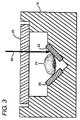
- deposited layer 32 when it is desired to create a buffer layer from deposited layer 32, deposited layer 32 must be impinged by, preferably, a laser beam 40 from a conventional 1000W CO2 laser (notshown).
- substrate 4 with deposited layer 32 is mounted on a conventional heater block 42 which, in turn, is mounted on a conventional X-Y traverse 44.
- Laser beam 40 is then impinged upon layer 32 at a wavelength, preferably, of about 10 ⁇ m so that the (100) faces of all of the SiTi03 molecules in the layer 32 are more precisely oriented with respect to substrate 4 such that the (100) faces are fairly precisely parallel to the plane of the surface of substrate 4 upon which layer 32 is deposited.
- This laser treatment further increases the precision of the orientation of the (100) faces of layer 32.
- Figure 5a shows a standard rocking curve for a SrTi03 film about the (200) peak.
- the rocking curve was measured around the strong peak of (200).
- the (100) behavior is essentially the same.
- a scan be seen, prior to laser treatment, a majority of the SrTi03 deposit has a lattice structure whose angular orientation (theta) with respect to the substrate surface is distributed with a peak around 22°. Consequently, when the YBCO is deposited on layer 32, the randomness of the orientation of the (100) faces of the SiTi03 layer may create a lack of alignment of the c-axis in the YBCO layer which can, ultimately, affect the superconductive properties of the YBCO layer.
- Figure 5b shows that once once layer is recrystallized by localized transient heating, the lack of uniformity of the orientation of the (100) faces virtually disappears. It so happened that the measurement after recrystallization was carried around the (100) peak, but the behavior of the (200) peak is the same.
- Figure 5b shows that after recrystallization, the rocking curve about the (100) peak of almost all of the SiTi03 film is concentrated around 12° with a very narrow spread therefrom.
- a preferred localized heat source is used which consists of a CO2 laser with output at 10.6 ⁇ m.
- the CO2 laser is advantageous because it provides an intense controllable pattern that is strongly absorbed by SrTiO3. Consequently, this improvement in orientation allows the YBCO molecules in superconductor layers to fairly accurately align along the length of the YBCO layer and increase the superconductive properties of the YBCO layer.
- layer 32 need not be laser treated.
- the capacitance properties of layer 32 as originally manufactured prior to laser treatment are sufficient to create a high density capacitor.
- the dielectric constant parallel to the axis normal to the (100) face (for simplicity we refer to this as the c-axis) of a SiTi03 molecule (190 at 26 degrees K and 100 KHz) is approximately twice the value along either of the other axes (85 for the same conditions imposed on the c-axis).
- the SrTiO3 is such that the SrTiO3 is capable of being initially laser treated with laser ablation to create a buffer layer or a high density capacitor and subsequently laser treated with the CO2 laser to further create a highly conductive superconductor substrate. This is because the SrTiO3 has a strong absorption rate at the wavelength where the excimer and CO2 lasers operate, which are approximately 0.2 ⁇ m and 10.6 ⁇ m, respectively.
Landscapes
- Engineering & Computer Science (AREA)
- Manufacturing & Machinery (AREA)
- Physical Vapour Deposition (AREA)
- Superconductors And Manufacturing Methods Therefor (AREA)
- Crystals, And After-Treatments Of Crystals (AREA)
Applications Claiming Priority (2)
| Application Number | Priority Date | Filing Date | Title |
|---|---|---|---|
| US69549291A | 1991-05-02 | 1991-05-02 | |
| US695492 | 1991-05-02 |
Publications (2)
| Publication Number | Publication Date |
|---|---|
| EP0512679A2 true EP0512679A2 (fr) | 1992-11-11 |
| EP0512679A3 EP0512679A3 (en) | 1993-01-27 |
Family
ID=24793220
Family Applications (1)
| Application Number | Title | Priority Date | Filing Date |
|---|---|---|---|
| EP19920302810 Withdrawn EP0512679A3 (en) | 1991-05-02 | 1992-03-31 | Method of making laser ablated oriented films on metal substrates and articles formed thereby |
Country Status (2)
| Country | Link |
|---|---|
| EP (1) | EP0512679A3 (fr) |
| JP (1) | JPH05148621A (fr) |
Families Citing this family (1)
| Publication number | Priority date | Publication date | Assignee | Title |
|---|---|---|---|---|
| JPH08144041A (ja) * | 1994-11-17 | 1996-06-04 | Toppan Printing Co Ltd | 巻取り式真空蒸着装置 |
Family Cites Families (7)
| Publication number | Priority date | Publication date | Assignee | Title |
|---|---|---|---|---|
| CA1326976C (fr) * | 1987-05-26 | 1994-02-15 | Satoshi Takano | Element supraconducteur |
| JPS6424323A (en) * | 1987-07-21 | 1989-01-26 | Sumitomo Electric Industries | Manufacture of superconductor thin film |
| JP2532914B2 (ja) * | 1988-03-31 | 1996-09-11 | 三井金属鉱業株式会社 | 超電導セラミックス積層体およびその製造法 |
| US5108982A (en) * | 1988-12-22 | 1992-04-28 | General Atomics | Apparatus and method for manufacturing a ceramic superconductor coated metal fiber |
| JPH02197565A (ja) * | 1989-01-25 | 1990-08-06 | Fujikura Ltd | レーザ蒸着装置用ターゲット |
| JPH02258698A (ja) * | 1989-03-31 | 1990-10-19 | Kokusai Chiyoudendou Sangyo Gijutsu Kenkyu Center | 酸化物超電導体の製造方法 |
| WO1991014028A1 (fr) * | 1990-03-16 | 1991-09-19 | Conductus, Inc. | Films supraconducteurs a haute temperature sur substrats d'oxyde d'aluminium |
-
1992
- 1992-03-31 EP EP19920302810 patent/EP0512679A3/en not_active Withdrawn
- 1992-04-22 JP JP4101489A patent/JPH05148621A/ja active Pending
Also Published As
| Publication number | Publication date |
|---|---|
| EP0512679A3 (en) | 1993-01-27 |
| JPH05148621A (ja) | 1993-06-15 |
Similar Documents
| Publication | Publication Date | Title |
|---|---|---|
| CA2560771C (fr) | Depot de film a texture biaxiale pour rubans revetus de supraconducteurs | |
| US5356474A (en) | Apparatus and method for making aligned Hi-Tc tape superconductors | |
| US5432151A (en) | Process for ion-assisted laser deposition of biaxially textured layer on substrate | |
| US5872080A (en) | High temperature superconducting thick films | |
| US5968877A (en) | High Tc YBCO superconductor deposited on biaxially textured Ni substrate | |
| KR100683186B1 (ko) | 다층 제품 및 그의 제조방법 | |
| US6624122B1 (en) | High critical current superconducting tapes | |
| US20040028954A1 (en) | High temperature superconducting thick films | |
| US7736761B2 (en) | Buffer layer for thin film structures | |
| US6884527B2 (en) | Biaxially textured composite substrates | |
| Ma et al. | Pulsed laser deposition of YBCO films on ISD MgO buffered metal tapes | |
| EP0512679A2 (fr) | Méthode de fabrication de films orientés par ablation par laser sur substrats métalliques et articles ainsi obtenus | |
| Ishimaru et al. | Observation of barrier recrystallization process and properties of ramp-edge Josephson junctions with interface-modified barrier | |
| EP0507539A2 (fr) | Méthode pour la fabrication de films diélectriques orientés sur substrats métalliques et articles ainsi obtenus | |
| Yanase et al. | Epitaxial Growth of Ti1-xAl xN Buffer Layer for a Ferroelectric (Ba, Sr) TiO3 Capacitor on Si Substrate | |
| US20050039672A1 (en) | Methods for surface-biaxially-texturing amorphous films | |
| JPH06231940A (ja) | ABaCuO系超電導コイルおよびその製造方法 | |
| US20090036313A1 (en) | Coated superconducting materials | |
| RU2189090C2 (ru) | СПОСОБ ФОРМИРОВАНИЯ МНОГОСЛОЙНЫХ СТРУКТУР ИЗ МАТЕРИАЛА YВaСuО С ДВУХ СТОРОН ПОДЛОЖКИ | |
| Ressler et al. | Ion Beam-Assisted Deposition of Biaxially Aligned CeO2 and ZrO2 Thin Films on Amorphous Substrates | |
| KR970009739B1 (ko) | 고온초전도박막의 제조방법 | |
| Ma et al. | Ion-beam-assisted deposition of biaxially aligned yttria-stabilized zirconia template films on metallic substrates for YBCO-coated conductors | |
| US20070026136A1 (en) | Process for improvement of IBAD texturing on substrates in a continuous mode | |
| Chakalov et al. | Influence of process parameters on the growth of YBCO thin films deposited by excimer laser ablation | |
| Tachikawa et al. | High-Tc superconducting films of Y-Ba-Cu oxide prepared by a CO2 laser beam evaporation |
Legal Events
| Date | Code | Title | Description |
|---|---|---|---|
| PUAI | Public reference made under article 153(3) epc to a published international application that has entered the european phase |
Free format text: ORIGINAL CODE: 0009012 |
|
| AK | Designated contracting states |
Kind code of ref document: A2 Designated state(s): DE GB NL |
|
| PUAL | Search report despatched |
Free format text: ORIGINAL CODE: 0009013 |
|
| AK | Designated contracting states |
Kind code of ref document: A3 Designated state(s): DE GB NL |
|
| STAA | Information on the status of an ep patent application or granted ep patent |
Free format text: STATUS: THE APPLICATION IS DEEMED TO BE WITHDRAWN |
|
| 18D | Application deemed to be withdrawn |
Effective date: 19931228 |