EP0512795B1 - Komparator für über den gesamten Versorgungsspannungsbereich sich erstreckende Eingangs-/Ausgangssignale - Google Patents
Komparator für über den gesamten Versorgungsspannungsbereich sich erstreckende Eingangs-/Ausgangssignale Download PDFInfo
- Publication number
- EP0512795B1 EP0512795B1 EP92304046A EP92304046A EP0512795B1 EP 0512795 B1 EP0512795 B1 EP 0512795B1 EP 92304046 A EP92304046 A EP 92304046A EP 92304046 A EP92304046 A EP 92304046A EP 0512795 B1 EP0512795 B1 EP 0512795B1
- Authority
- EP
- European Patent Office
- Prior art keywords
- stage
- type
- output
- differential
- gate
- Prior art date
- Legal status (The legal status is an assumption and is not a legal conclusion. Google has not performed a legal analysis and makes no representation as to the accuracy of the status listed.)
- Expired - Lifetime
Links
- 230000008878 coupling Effects 0.000 claims description 10
- 238000010168 coupling process Methods 0.000 claims description 10
- 238000005859 coupling reaction Methods 0.000 claims description 10
- 230000005669 field effect Effects 0.000 claims description 4
- 239000008186 active pharmaceutical agent Substances 0.000 description 6
- 238000012358 sourcing Methods 0.000 description 3
- 230000000295 complement effect Effects 0.000 description 2
- 238000010586 diagram Methods 0.000 description 2
- 238000012886 linear function Methods 0.000 description 2
- 230000002457 bidirectional effect Effects 0.000 description 1
- 230000003247 decreasing effect Effects 0.000 description 1
- 238000011084 recovery Methods 0.000 description 1
Images
Classifications
-
- H—ELECTRICITY
- H03—ELECTRONIC CIRCUITRY
- H03F—AMPLIFIERS
- H03F3/00—Amplifiers with only discharge tubes or only semiconductor devices as amplifying elements
- H03F3/45—Differential amplifiers
- H03F3/45071—Differential amplifiers with semiconductor devices only
- H03F3/45076—Differential amplifiers with semiconductor devices only characterised by the way of implementation of the active amplifying circuit in the differential amplifier
- H03F3/45179—Differential amplifiers with semiconductor devices only characterised by the way of implementation of the active amplifying circuit in the differential amplifier using MOSFET transistors as the active amplifying circuit
- H03F3/4521—Complementary long tailed pairs having parallel inputs and being supplied in parallel
-
- H—ELECTRICITY
- H03—ELECTRONIC CIRCUITRY
- H03F—AMPLIFIERS
- H03F3/00—Amplifiers with only discharge tubes or only semiconductor devices as amplifying elements
- H03F3/30—Single-ended push-pull [SEPP] amplifiers; Phase-splitters therefor
- H03F3/3001—Single-ended push-pull [SEPP] amplifiers; Phase-splitters therefor with field-effect transistors
- H03F3/3022—CMOS common source output SEPP amplifiers
- H03F3/3028—CMOS common source output SEPP amplifiers with symmetrical driving of the end stage
- H03F3/303—CMOS common source output SEPP amplifiers with symmetrical driving of the end stage using opamps as driving stages
-
- H—ELECTRICITY
- H03—ELECTRONIC CIRCUITRY
- H03F—AMPLIFIERS
- H03F2203/00—Indexing scheme relating to amplifiers with only discharge tubes or only semiconductor devices as amplifying elements covered by H03F3/00
- H03F2203/30—Indexing scheme relating to single-ended push-pull [SEPP]; Phase-splitters therefor
- H03F2203/30057—Indexing scheme relating to single-ended push-pull [SEPP]; Phase-splitters therefor the SEPP power transistors are realised as paralleled FETs, i.e. the push or the pull transistor
-
- H—ELECTRICITY
- H03—ELECTRONIC CIRCUITRY
- H03F—AMPLIFIERS
- H03F2203/00—Indexing scheme relating to amplifiers with only discharge tubes or only semiconductor devices as amplifying elements covered by H03F3/00
- H03F2203/45—Indexing scheme relating to differential amplifiers
- H03F2203/45508—Indexing scheme relating to differential amplifiers the CSC comprising a voltage generating circuit as bias circuit for the CSC
-
- H—ELECTRICITY
- H03—ELECTRONIC CIRCUITRY
- H03F—AMPLIFIERS
- H03F2203/00—Indexing scheme relating to amplifiers with only discharge tubes or only semiconductor devices as amplifying elements covered by H03F3/00
- H03F2203/45—Indexing scheme relating to differential amplifiers
- H03F2203/45674—Indexing scheme relating to differential amplifiers the LC comprising one current mirror
Definitions
- This invention relates to a comparator circuit and, in particular, to a comparator circuit which is responsive to differential input signals ranging over the full operating potential (i.e. from rail to rail) and which is capable of producing output signals which can swing from rail to rail (i.e. over the full range of the operating potential applied to the comparator circuit).
- a circuit designed to respond to differential input signals ranging over the full operating potential aplied to the circuit is shown, for example, in U.S. Patent 4,377,789 titled "Operational Amplifier Employing Complementary Field-Effect Transistors" issued to M.V. Hoover.
- the output of the circuit in the Hoover (4,37,789) patent does not swing from rail-to-rail (i.e. from V DD to V SS ).
- the output is limited to a value of V DD minus the threshhold voltage of a P-type transistor and to a value of V SS plus the threshhold voltage of an N-type transistor.
- the inability to produce output signals which swing all the way to V DD or V SS is problematic. For example, such an output can not drive a subsequent CMOS logic circuit properly, resulting in unwanted and undesirable power dissipation.
- the 4,333,058 includes a first differential amplifier stage (10) comprised of differentially connected transistors (P1, P2) and N-type load transistors (N3, N4) driving a current sinking transistor (N5) and a second differential amplifier stage (30) comprised of differentially connected N-type transistors (N1, N2) and P-type load transistors (P3, P4) driving a current sourcing transistor (P5).
- the same differential input signals are applied to the two differential amplifier stages (10 and 30).
- the first differential amplifier stage (10) When the differential signals are within a P-threshhold voltage (V TP ) of the most positive operating voltage (V+), the first differential amplifier stage (10) is inoperative in that both P1 and P2 are turned-off. Current sinking transistor N5 is then either off or in an indeterminate state. Concurrently, the second differential amplifier stage 30 is operative driving current sourcing transistor P5 as a function of the differential input signal. However, since N5 is off or indeterminate, the output response of the amplifier is not a true or linear function of the differential input signal.
- the second differential amplifier stage (30) is inoperative in that both N1 and N2 are turned-off.
- Current sourcing transistor P5 is then off or in an indeterminate state.
- the first differential amplifier stage (10) is operative driving the current sinking transistor N5 as a function of the input signal.
- P5 since P5 is off or indeterminate, the ouput response of the amplifier is not a true or linear function of the differential input signal.
- JP-A 61 234 110 discloses a comparator comprising: an n-type differential circuit and a p-type differential circuit both receiving the same differential input signals; whereby the n-type differential circuit is responsive to differential input signals ranging in value between V1 and a n-threshold voltage level > OV for producing output signals which can swing fully between the power supply voltages as a function of the differential input signal and whereby the p-type circuit is responsive to differential input signals ranging in value between OV and a second voltage level which is a p-threshold voltage below the positive power supply voltage, for producing output signals which can swing fully between the power supply voltages as a function of the differential input signal; and means for combining the output signals of said first and second stages for producing output signals which can swing between the power supply voltages for values of differential input signals which range between the power supply voltages.
- the invention consists in a comparator comprising:
- Insulated-gate field-effect transistors are the active devices preferred for use in practicing the invention. for this reason, the circuit is illustrated in the drawing as employing such transistors and will be so described hereinafter. However, this is not intended to preclude the use of other suitable devices and to this end, the term "transistor” when used without limitation in the appended claims, is used in a generic sense.
- enhancement type IGFETs of P conductivity type are identified by the letter P followed by a particular reference character; and enhancement type IGFETs of N-conductivity type are identified by the letter N followed by a particular reference character.
- the characteristics of IGFETs are well known and need not be described in detail. But, for a clearer understanding of the description to follow, definition and characteristics of IGFETs pertinent to the invention are set forth below.
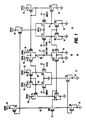
- FIGURE 1 there is shown a first and second complementary differential amplifier stages 11 and 13, respectively, whose outputs are coupled to an OR'ing circuit 15 for producing an output signal 05 at output terminal 17 which can swing virtually over the full operating voltages (Vdd and Vss) applied to amplifier stages 11 and 13.
- the first differential amplifier stage 11 includes IGFETS N1 and N2 having their source electrodes connected in common to the drain of an IGFET N3 which is biased to function as a relatively constant current source.
- the source of N3 is connected to power terminal 16 to which is applied the most negative potential, Vss, which in the FIGURE is set to ground potential.
- Input signals V1 and V2 are applied to the gate electrodes of N1 and N2, respectively.
- the drains of N1 and N2 are connected to output nodes O1 and O2, respectively.
- Two P-type transistors, PL1 and PL2, which function as load devices have their conduction paths connected between a power terminal 18 and terminal 01 and 02, respectively.
- the most positive operating potential denoted as Vdd is applied to terminal 18.
- the gates of PL1 and PL2 are connected in common to the drains of PL1 and N1 at output terminal 01.
- the second differential amplifier stage 13 includes IGFETs P1 and P2 having their source electrodes connected in common to the drain of P3 which is biased to function as a relatively constant current source.
- the source of P3 is connected to Vdd.
- the input signals V1 and V2 are applied to the gate electrodes of P2 and P1, respectively.
- the drains of P1 and P2 are respectively connected to output nodes 03 and 04.
- Two N-type transistors, NL1 and NL2, which function as load devices, have their conduction paths connected between terminal 16 and output terminals 03 and 04, respectively.
- the gates of NL1 and NL2 are connected in common to the drains of P1 and NL1 at output 03.
- the OR'ing circuit 15 includes IGFETS N4 and P4 respectively driven from the outputs O1 and O2 of stage 11 and IGFETS N5 and P5 respectively driven from the outputs O3 and O4 of stage 13.
- the output O1 is connected to the gate of P6 whose source is connected to Vdd.
- the drain of P6 is connected to the drain and gate of N6 and the gate of N4.
- the sources of N6 and N4 are grounded.
- the drain of N4 is connected to output terminal 17.
- PL1, P6, N6 and N4 function to mirror the current (IN1) flowing in N1 via the conduction path of N4 into or out of output O5.
- the output O2 is directly connected to the gate of P4 whose source is connected to Vdd and whose drain is connected to terminal 17.
- the output O3 is directly connected to the gate of N5 whose source is grounded and whose drain is connected to output terminal 17.
- the output O4 is connected to the gate of N7 whose drain is connected to the gate and drain of P7 and to the gate of P5.
- the source of N7 is returned to ground and the sources of P7 and P5 are returned to Vdd.
- the drain of P5 is connected to terminal 17.
- the current (IP2) flowing in P2 and NL2 is mirrored via N7, P7 and the conduction path of P5 into or out of the output O5.
- the bias circuit for current sources P3 and N3 includes a "diode” connected transistor P8 whose source is returned to Vdd and whose gate and drain are connected in common to the gate of P3 and via a resistor R1 to the drain of a transistor N9.
- the source of N9 is connected to the gate and drain of "diode” connected N8 and the gate of N3.
- the source of N8 is returned to ground.
- a power down (on/off control) signal is applied to the gate of N9. When the control signal applied to the gate of N9 is "low” there is no conduction in P8 and/or N8 whereby Vdd is applied to the gate of P3 and ground is applied to the gate of N3.
- P3 and N3 are then not conducting and the differential stages 11 and 13 are off and not operable.
- the circuit of Figure 1 is rendered operable when the control (Power Down) signal goes "high" turning on N9 and causing conduction in P8 and N8.
- the voltage drop across P8 is aplied to the gate of P3 causing P3 to conduct as a relatively constant current source.
- the voltage drop across N8 is applied to the gate of N3 causing N3 to conduct and function as a relatively constant current source.
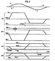
- the operation of the circuit of FIGURE 1 is such that when V1 is more positive than V2, transistors N4 and N5 are driven into a higher conductivity (lower impedance) condition and transistors P4 and P5 are driven into a lower conductivity (higher impedance) condition. It is significant that at least one of transistors N4 and N5 is driven such that the output O5 can be driven to, or close to, ground potential.
- transistors P4 and P5 are driven into a higher conductivity (lower impedance) condition and transistors N4 and N5 are driven into a lower conductivity (higher impedance) condition. It is significant that at least one of P4 and P5 is driven such that the output can be driven to, or close to, Vdd volts.
- differential amplifier stage 11 which includes differentially connected transistors N1 and N2 and load transistors PL1 and PL2, is operative for values of V1 and V2 which are more positive than an N-threshold voltage (V TN ) above the voltage at terminal 16, which in FIGURE 1 is ground potential.
- V TN N-threshold voltage
- N1 and N2 are non-conducting even if there is a difference between V1 and V2. for such values of V1 and V2, the output signals at O1 and O2 are at, or close to, V DD volts (or indeterminate).
- differential amplifier stage 11 produces difference signals at outputs O1 and O2 which are a function of the amplitude of the difference between input signals V1 and V2.
- the output signals EO1 and EO2 produced at outputs O1 and O2 are used to drive the gates of IGFETS P4 and N4 which produce an output at terminal 17 which is proportional to the differential input (V1-V2) and which output can swing between V DD (the voltage at rail 18) and ground (the voltage at rail 16).
- the differential amplifier stage 13 which includes differentially connected transistors P1 and P2 and load transistors NL1 and NL2, is inoperative for values of V1 and V2 which is between V DD volts and a P-threshold voltage (V TP ) of V DD volts. for such values of V1 and V2, the output signals EO3 and EO4 produced at outputs O1 and O2 are at, or close to, ground potential (or indeterminate).
- differential amplifier 13 For values of V1 and V2 which are less positive than V TP volts below V DD volts, differential amplifier 13 is operative. for these values of input signals (i.e. V DD - V TP > V1 and/or V2) transistors P1 and P2 produce differential signals EO3 and EO4, at outputs O3 and O4, which are representative of the differential input signals (V1 - V2). EO3 and EO4 are in turn used to supply the potentials applied to the gates of P5 and N5 which produce an output at terminal 17 which is proportional to the differential input signal (V1 - V2) and which output can swing between V DD and ground.
Landscapes
- Engineering & Computer Science (AREA)
- Power Engineering (AREA)
- Amplifiers (AREA)
- Manipulation Of Pulses (AREA)
Claims (5)
- Vergleicher, der folgendes umfasst:erste und zweite Netzleitungen, um eine erste Netzspannung VP1 und eine zweite Netzspannung VP2 jeweils darauf anzuwenden; wobei VP1 positiver als VP2 ist;erste und zweite Differentialverstärkerstufen, wobei jede Stufe erste und zweite Eingangsanschlüsse, erste und zweite Ausgangsanschlüsse und erste und zweite Netzanschlüsse hat;ein Mittel, um die ersten Netzanschlüsse der ersten und zweiten Stufen an die erste Netzleitung anzuschließen, und die zweiten Netzanschlüsse der ersten und zweiten Stufen an die zweite Netzleitung anzuschließen;ein Mittel, um dieselben Differentialeingangssignale über die ersten und zweiten Signaleingangsanschlüsse der ersten und zweiten Stufen anzuwenden;wobei die erste Stufe auf Differentialeingangssignale reagiert, die sich im Wert von VP1 bis zu einem ersten Spannungsstand erstrecken, der VT1 Volt über VP2 liegt, um Ausgangssignale herzustellen, die völlig zwischen VP1 und VP2 als eine Funktion des Differentialeingangssignals schwingen können;wobei die zweite Stufe auf Differentialeingangssignale reagiert, die sich im Wert von VP2 bis zu einem zweiten Spannungsstand erstrecken, der VT2 Volt unter VP1 liegt, um Ausgangssignale herzustellen, die völlig zwischen VP1 und VP2 als eine Funktion Cf des Differentialeingangssignals schwingen können; undein Mittel zum Kombinieren der Ausgangssignale der ersten und zweiten Stufen, um Ausgangssignale herzustellen, die zwischen VP1 und VP2 für Werte von Differentialeingangssignalen schwingen können, die sich von VP1 bis VP2 erstrecken, das folgendes einschließt:a) erste und zweite P-IGFETS, die ihre Leitungswege parallel zwischen einer ersten Betriebspotentialstelle und einem Ausgangsanschluß angeschlossen haben;b) erste und zweite N-IGFETS, die ihre Leitungswege parallel zwischen dem Ausgangsanschluß und einer zweiten Betriebspotentialstelle angeschlossen haben;c) ein Mittel, das die ersten und zweiten Ausgänge der ersten Differentialverstärkerstufe an die Gatter des ersten P-IGFETs und des ersten N-IGFETs anschließt; undd) ein Mittel, das die ersten und zweiten Ausgänge der zweiten Differentialverstärkerstufe an die Gatter des zweiten P-IGFETs und an das Gatter des zweiten N-IGFETs anschließt.
- Vergleicher nach Anspruch 1, in dem die erste Differentialverstärkerstufe aktive differential angeschlossene Transistoren einer Leitungsart einschließt, die an Lasttransistoren der entgegengesetzten Leitungsart angeschlossen sind;und in dem die zweite Differentialverstärkerstufe aktive differential angeschlossene Transistoren der entgegengesetzten Leitungsart einschließt, die an Lasttransistoren der einen Leitungsart angeschlossen sind.
- Vergleicher nach Anspruch 2,wobei das Mittel des Anschlusses der ersten und zweiten Ausgänge der ersten Differentialverstärkerstufe an die Gatter des ersten P-IGFETs und des ersten N-IGFETs folgendes einschließt:c1) ein Mittel zum Gleichstromanschluß des ersten Ausgangs des ersten Differentialverstärkers an das Gatter des ersten P-IGFETs, undc2) ein Mittel, das eine Stromspiegelschaltung einschließt, um den zweiten Ausgang der ersten Differentialverstärkerstufe an das Gatter des ersten N-IGFETs anzuschließen; und wobei das Mittel, um die ersten und zweiten Ausgänge der zweiten Differentialverstärkerstufe an die Gatter des zweiten P-IGFETs und des zweiten N-IGFETs anzuschließen, folgendes einschließt:d1) ein Mittel zum Gleichstromanschluß des ersten Ausgangs des zweiten Differentialverstärkers an das Gatter des zweiten N-IGFETs, undd2) ein Mittel, das eine Stromspiegelschaltung einschließt, um den zweiten Ausgang der zweiten Differentialverstärkerstufe an das Gatter des zweiten P-IGFETs anzuschließen.
- Vergleicherschaltung nach Anspruch 3, in der die erste Stufe ein Paar differential angeschlossene Transistoren der N-Leitungsart einschließt, und die zweite Stufe ein Paar differential angeschlossene Transistoren der P-Leitungsart einschließt.
- Vergleicher nach Anspruch 4, in dem die erste Stufe folgendes einschließt:erste und zweite differential angeschlossene Isolierschicht-Feldeffekttransistoren IGFETs der N-Leitungsart, wobei der erste differential angschlossene N-Transistor sein Gatter an den ersten Signaleingangsanschluß der ersten Stufe angeschlossen hat, und seinen Leitungsweg zwischen dem ersten Signalausgangsanschluß der ersten Stufe und einem Differentialknotenpunkt der ersten Stufe angeschlossen hat, und der zweite differential angeschlossene N-Transistor sein Gatter an den zweiten Signaleingangsanschluß der ersten Stufe angeschlossen hat, und seinen Leitungsweg zwischen dem zweiten Signalausgangsanschluß der ersten Stufe und dem Differentialknotenpunkt der ersten Stufe angeschlossen hat;eine relativ konstante Stromquelle, die zwischen dem Differentialknotenpunkt der ersten Stufe und der Netzleitung angeschlossen ist; undeinen ersten Lasttransistor der P-Leitungsart, der seinen Leitungsweg zwischen dem ersten Ausgang der ersten Stufe und der ersten Netzleitung angeschlossen hat, und einen zweiten Lasttransistor der P-Leitungsart, der seinen Leitungsweg zwischen dem zweiten Ausgang der ersten Stufe und der ersten Netzleitung angeschlossen hat; und wobei die zweite Stufe folgendes einschließt:erste und zweite differential angeschlossene Transistoren der P-Leitungsart, wobei der erste differential angeschlossene P-Transistor sein Gatter an den ersten Signaleingangsanschluß der zweiten Stufe angeschlossen hat, und seinen Leitungsweg zwischen dem ersten Ausgangsanschluß der zweiten Stufe und dem Differentialknotenpunkt der zweiten Stufe angeschlossen hat, und der zweite differential angeschlossene P-Transistor sein Gatter an den zweiten Signaleingangsanschluß des zweiten Ausgangsanschlusses der zweiten Stufe und dem Differentialknotenpunkt der zweiten Stufe angeschlossen hat;eine relativ konstante Stromquelle, die zwischen dem Differentialknotenpunkt der zweiten Stufe und der ersten Netzleitung angeschlossen ist; undeinen ersten Lasttransistor der N-Leitungsart, der seinen Leitungsweg zwischen dem ersten Signalausgangsanschluß der zweiten Stufe und der zweiten Netzleitung angeschlossen hat, und einen zweiten Lasttransistor der N-Leitungsart, der seinen Leitungsweg zwischen dem zweiten Signalausgangsanschluß der zweiten Stufe und der ersten Netzleitung angeschlossen hat.
Applications Claiming Priority (2)
| Application Number | Priority Date | Filing Date | Title |
|---|---|---|---|
| US07/696,481 US5142244A (en) | 1991-05-06 | 1991-05-06 | Full range input/output comparator |
| US696481 | 2000-10-24 |
Publications (3)
| Publication Number | Publication Date |
|---|---|
| EP0512795A2 EP0512795A2 (de) | 1992-11-11 |
| EP0512795A3 EP0512795A3 (en) | 1994-05-11 |
| EP0512795B1 true EP0512795B1 (de) | 1996-08-21 |
Family
ID=24797253
Family Applications (1)
| Application Number | Title | Priority Date | Filing Date |
|---|---|---|---|
| EP92304046A Expired - Lifetime EP0512795B1 (de) | 1991-05-06 | 1992-05-05 | Komparator für über den gesamten Versorgungsspannungsbereich sich erstreckende Eingangs-/Ausgangssignale |
Country Status (4)
| Country | Link |
|---|---|
| US (1) | US5142244A (de) |
| EP (1) | EP0512795B1 (de) |
| JP (1) | JPH05206798A (de) |
| DE (1) | DE69212886T2 (de) |
Families Citing this family (35)
| Publication number | Priority date | Publication date | Assignee | Title |
|---|---|---|---|---|
| USRE38482E1 (en) * | 1992-05-28 | 2004-03-30 | Rambus Inc. | Delay stage circuitry for a ring oscillator |
| US5485490A (en) * | 1992-05-28 | 1996-01-16 | Rambus, Inc. | Method and circuitry for clock synchronization |
| US5349304A (en) * | 1993-02-12 | 1994-09-20 | Sgs-Thomson Microelectronics, Inc. | Operational amplifier having multiple positive inputs |
| US5384548A (en) * | 1993-08-25 | 1995-01-24 | The Ohio State University | Constant transconductance bias circuit and method |
| US5621339A (en) * | 1993-09-14 | 1997-04-15 | Crystal Semiconductor | Method and apparatus for removing trapped oxide charge from a differential input stage |
| DE19521089C1 (de) * | 1995-06-09 | 1996-08-08 | Siemens Ag | Schaltungsanordnung zur Realisierung von durch Schwellenwertgleichungen darstellbaren Logikelementen |
| US5714906A (en) * | 1995-08-14 | 1998-02-03 | Motamed; Ali | Constant transductance input stage and integrated circuit implementations thereof |
| FR2738424B1 (fr) * | 1995-09-05 | 1997-11-21 | Sgs Thomson Microelectronics | Interrupteur analogique basse tension |
| JP3392271B2 (ja) * | 1995-11-02 | 2003-03-31 | シャープ株式会社 | 演算増幅回路 |
| US5726592A (en) * | 1995-12-18 | 1998-03-10 | International Business Machines Corporation | Self biased low-voltage differential signal detector |
| JPH09232883A (ja) * | 1996-02-23 | 1997-09-05 | Oki Micro Design Miyazaki:Kk | 演算増幅回路 |
| US5801564A (en) * | 1996-06-28 | 1998-09-01 | Symbios, Inc. | Reduced skew differential receiver |
| US5889419A (en) * | 1996-11-01 | 1999-03-30 | Lucent Technologies Inc. | Differential comparison circuit having improved common mode range |
| FR2762161B1 (fr) * | 1997-04-15 | 1999-07-02 | Sgs Thomson Microelectronics | Comparateur a grande excursion de tension d'entree |
| FR2764752B1 (fr) * | 1997-06-16 | 1999-08-13 | Sgs Thomson Microelectronics | Etage d'entrees differentielles pour reception large bande avec forte rejection de mode commun |
| DE69731088D1 (de) | 1997-10-31 | 2004-11-11 | St Microelectronics Srl | Ausgangsstufe mit hoher Versorgungsspannung zum Steuern einer elektrischen Last |
| JP2000014179A (ja) * | 1998-06-24 | 2000-01-14 | Aisin Seiki Co Ltd | 電気モータの1相コイルの通電/非通電制御装置における異常検出装置 |
| FR2782584B1 (fr) * | 1998-08-19 | 2000-11-03 | St Microelectronics Sa | Comparateur en technologie bicmos a faible tension d'alimentation |
| US6038266A (en) * | 1998-09-30 | 2000-03-14 | Lucent Technologies, Inc. | Mixed mode adaptive analog receive architecture for data communications |
| US6198420B1 (en) * | 1998-12-14 | 2001-03-06 | Silicon Systems Research Limited | Multiple level quantizer |
| US6448821B1 (en) * | 2000-02-25 | 2002-09-10 | National Semiconductor Corporation | Comparator circuit for comparing differential input signal with reference signal and method |
| US6617921B2 (en) * | 2000-11-20 | 2003-09-09 | Texas Instruments Incorporated | High output swing comparator stage |
| US6611160B1 (en) * | 2000-11-21 | 2003-08-26 | Skyworks Solutions, Inc. | Charge pump having reduced switching noise |
| US6486710B1 (en) * | 2001-06-29 | 2002-11-26 | Intel Corporation | Differential voltage magnitude comparator |
| TW557633B (en) * | 2001-10-30 | 2003-10-11 | Faraday Tech Corp | Noise-reduction circuit capable of adjusting input level |
| US6844781B1 (en) | 2003-07-07 | 2005-01-18 | Ami Semiconductor, Inc. | Dual differential-input amplifier having wide input range |
| US7061322B2 (en) * | 2004-06-15 | 2006-06-13 | Promos Technologies Inc. | Low voltage differential amplifier circuit and bias control technique enabling accommodation of an increased range of input levels |
| US7167052B2 (en) * | 2004-06-15 | 2007-01-23 | Promos Technologies Inc. | Low voltage differential amplifier circuit for wide voltage range operation |
| US7102439B2 (en) * | 2004-06-15 | 2006-09-05 | Promos Technologies Inc. | Low voltage differential amplifier circuit and a sampled low power bias control technique enabling accommodation of an increased range of input levels |
| US7592844B2 (en) * | 2007-01-19 | 2009-09-22 | Power Integrations, Inc. | Comparator with complementary differential input stages |
| US8330501B1 (en) * | 2010-10-19 | 2012-12-11 | Xilinx, Inc. | Dual mode rail-to-rail buffer for low voltage memory |
| CN106612112B (zh) | 2015-10-21 | 2022-02-08 | 恩智浦美国有限公司 | 具有共享有源负载的轨对轨比较器 |
| US9903121B2 (en) * | 2016-06-06 | 2018-02-27 | Morryde International, Inc. | Folding staircase |
| US9771025B1 (en) | 2016-06-17 | 2017-09-26 | Lippert Components, Inc. | Stowable stair carrier with lift assist mechanism |
| EP3910795A1 (de) * | 2020-05-13 | 2021-11-17 | ams International AG | Komparatorschaltung |
Family Cites Families (9)
| Publication number | Priority date | Publication date | Assignee | Title |
|---|---|---|---|---|
| US4333058A (en) * | 1980-04-28 | 1982-06-01 | Rca Corporation | Operational amplifier employing complementary field-effect transistors |
| US4377789A (en) * | 1981-03-20 | 1983-03-22 | Rca Corporation | Operational amplifier employing complementary field-effect transistors |
| US4585961A (en) * | 1984-01-19 | 1986-04-29 | At&T Bell Laboratories | Semiconductor integrated circuit for squaring a signal with suppression of the linear component |
| US4554515A (en) * | 1984-07-06 | 1985-11-19 | At&T Laboratories | CMOS Operational amplifier |
| JPS61234110A (ja) * | 1985-04-09 | 1986-10-18 | Toshiba Corp | 差動回路 |
| CA1260080A (en) * | 1986-09-10 | 1989-09-26 | Akira Yukawa | Operational amplifier circuit having wide operating range |
| KR910009557B1 (ko) * | 1987-03-31 | 1991-11-21 | 미쓰비시 뎅끼 가부시끼가이샤 | 동기신호 처리회로 |
| US4825100A (en) * | 1988-04-04 | 1989-04-25 | Tektronix, Inc. | High speed R-S latch |
| US4859961A (en) * | 1988-12-19 | 1989-08-22 | Triouint Semiconductor, Inc. | Wide bandwidth push-pull parallel amplifier |
-
1991
- 1991-05-06 US US07/696,481 patent/US5142244A/en not_active Expired - Lifetime
-
1992
- 1992-03-25 JP JP4098902A patent/JPH05206798A/ja active Pending
- 1992-05-05 EP EP92304046A patent/EP0512795B1/de not_active Expired - Lifetime
- 1992-05-05 DE DE69212886T patent/DE69212886T2/de not_active Expired - Fee Related
Also Published As
| Publication number | Publication date |
|---|---|
| EP0512795A2 (de) | 1992-11-11 |
| DE69212886T2 (de) | 1997-03-27 |
| DE69212886D1 (de) | 1996-09-26 |
| JPH05206798A (ja) | 1993-08-13 |
| US5142244A (en) | 1992-08-25 |
| EP0512795A3 (en) | 1994-05-11 |
Similar Documents
| Publication | Publication Date | Title |
|---|---|---|
| US5142244A (en) | Full range input/output comparator | |
| US4501978A (en) | Level shift interface circuit | |
| US5206544A (en) | CMOS off-chip driver with reduced signal swing and reduced power supply disturbance | |
| EP0168198B1 (de) | CMOS-Operationsverstärker | |
| US5350957A (en) | Electronic switch controlled by plural inputs | |
| US5920204A (en) | On/off control for a balanced differential current mode driver | |
| US6252435B1 (en) | Complementary differential amplifier with resistive loads for wide common-mode input range | |
| US4707623A (en) | CMOS input level shifting buffer circuit | |
| US5334883A (en) | Circuit for introducing hysterisis | |
| KR100245902B1 (ko) | 캐스코드 상보형 금속 산화물 반도체 증폭기의 안정화 과도 응답 | |
| EP0308000A1 (de) | Verstärkerschaltung | |
| US4318015A (en) | Level shift circuit | |
| US4717847A (en) | TTL compatible CMOS input buffer | |
| US5155387A (en) | Circuit suitable for differential multiplexers and logic gates utilizing bipolar and field-effect transistors | |
| US4321491A (en) | Level shift circuit | |
| JP3301780B2 (ja) | 切換可能な電圧ジェネレータ及び演算増幅器 | |
| US5287068A (en) | Comparator amplifier | |
| JP3047869B2 (ja) | 出力振幅調整回路 | |
| JP3492765B2 (ja) | レベル変換回路 | |
| US5196737A (en) | Latching comparator employing transfer gates | |
| US6762646B1 (en) | Modified folded cascode amplifier | |
| US4383223A (en) | CMOS Operational amplifier employing push-pull output stage | |
| US4206418A (en) | Circuit for limiting voltage differential in differential amplifiers | |
| US6232805B1 (en) | Buffer circuit with voltage clamping and method | |
| US4788510A (en) | Differential input stage for differential line receivers and operational amplifiers |
Legal Events
| Date | Code | Title | Description |
|---|---|---|---|
| PUAI | Public reference made under article 153(3) epc to a published international application that has entered the european phase |
Free format text: ORIGINAL CODE: 0009012 |
|
| AK | Designated contracting states |
Kind code of ref document: A2 Designated state(s): DE FR GB SE |
|
| PUAL | Search report despatched |
Free format text: ORIGINAL CODE: 0009013 |
|
| AK | Designated contracting states |
Kind code of ref document: A3 Designated state(s): DE FR GB SE |
|
| 17P | Request for examination filed |
Effective date: 19941111 |
|
| 17Q | First examination report despatched |
Effective date: 19950518 |
|
| GRAH | Despatch of communication of intention to grant a patent |
Free format text: ORIGINAL CODE: EPIDOS IGRA |
|
| GRAH | Despatch of communication of intention to grant a patent |
Free format text: ORIGINAL CODE: EPIDOS IGRA |
|
| GRAA | (expected) grant |
Free format text: ORIGINAL CODE: 0009210 |
|
| AK | Designated contracting states |
Kind code of ref document: B1 Designated state(s): DE FR GB SE |
|
| ET | Fr: translation filed | ||
| REF | Corresponds to: |
Ref document number: 69212886 Country of ref document: DE Date of ref document: 19960926 |
|
| PG25 | Lapsed in a contracting state [announced via postgrant information from national office to epo] |
Ref country code: SE Effective date: 19961121 |
|
| PLBE | No opposition filed within time limit |
Free format text: ORIGINAL CODE: 0009261 |
|
| STAA | Information on the status of an ep patent application or granted ep patent |
Free format text: STATUS: NO OPPOSITION FILED WITHIN TIME LIMIT |
|
| 26N | No opposition filed | ||
| REG | Reference to a national code |
Ref country code: GB Ref legal event code: IF02 |
|
| PGFP | Annual fee paid to national office [announced via postgrant information from national office to epo] |
Ref country code: FR Payment date: 20020417 Year of fee payment: 11 |
|
| PGFP | Annual fee paid to national office [announced via postgrant information from national office to epo] |
Ref country code: GB Payment date: 20020501 Year of fee payment: 11 |
|
| PGFP | Annual fee paid to national office [announced via postgrant information from national office to epo] |
Ref country code: DE Payment date: 20020520 Year of fee payment: 11 |
|
| PG25 | Lapsed in a contracting state [announced via postgrant information from national office to epo] |
Ref country code: GB Free format text: LAPSE BECAUSE OF NON-PAYMENT OF DUE FEES Effective date: 20030505 |
|
| PG25 | Lapsed in a contracting state [announced via postgrant information from national office to epo] |
Ref country code: DE Free format text: LAPSE BECAUSE OF NON-PAYMENT OF DUE FEES Effective date: 20031202 |
|
| GBPC | Gb: european patent ceased through non-payment of renewal fee |
Effective date: 20030505 |
|
| PG25 | Lapsed in a contracting state [announced via postgrant information from national office to epo] |
Ref country code: FR Free format text: LAPSE BECAUSE OF NON-PAYMENT OF DUE FEES Effective date: 20040130 |
|
| REG | Reference to a national code |
Ref country code: FR Ref legal event code: ST |