EP0516480A2 - Verfahren zur Oberflächenbehandlung mit Ionenstrahlen extra niedriger Geschwindigkeit - Google Patents
Verfahren zur Oberflächenbehandlung mit Ionenstrahlen extra niedriger Geschwindigkeit Download PDFInfo
- Publication number
- EP0516480A2 EP0516480A2 EP92304964A EP92304964A EP0516480A2 EP 0516480 A2 EP0516480 A2 EP 0516480A2 EP 92304964 A EP92304964 A EP 92304964A EP 92304964 A EP92304964 A EP 92304964A EP 0516480 A2 EP0516480 A2 EP 0516480A2
- Authority
- EP
- European Patent Office
- Prior art keywords
- cluster
- ion beam
- surface treatment
- ions
- atoms
- Prior art date
- Legal status (The legal status is an assumption and is not a legal conclusion. Google has not performed a legal analysis and makes no representation as to the accuracy of the status listed.)
- Ceased
Links
Images




Classifications
-
- H—ELECTRICITY
- H10—SEMICONDUCTOR DEVICES; ELECTRIC SOLID-STATE DEVICES NOT OTHERWISE PROVIDED FOR
- H10P—GENERIC PROCESSES OR APPARATUS FOR THE MANUFACTURE OR TREATMENT OF DEVICES COVERED BY CLASS H10
- H10P30/00—Ion implantation into wafers, substrates or parts of devices
- H10P30/20—Ion implantation into wafers, substrates or parts of devices into semiconductor materials, e.g. for doping
- H10P30/21—Ion implantation into wafers, substrates or parts of devices into semiconductor materials, e.g. for doping of electrically active species
-
- C—CHEMISTRY; METALLURGY
- C23—COATING METALLIC MATERIAL; COATING MATERIAL WITH METALLIC MATERIAL; CHEMICAL SURFACE TREATMENT; DIFFUSION TREATMENT OF METALLIC MATERIAL; COATING BY VACUUM EVAPORATION, BY SPUTTERING, BY ION IMPLANTATION OR BY CHEMICAL VAPOUR DEPOSITION, IN GENERAL; INHIBITING CORROSION OF METALLIC MATERIAL OR INCRUSTATION IN GENERAL
- C23C—COATING METALLIC MATERIAL; COATING MATERIAL WITH METALLIC MATERIAL; SURFACE TREATMENT OF METALLIC MATERIAL BY DIFFUSION INTO THE SURFACE, BY CHEMICAL CONVERSION OR SUBSTITUTION; COATING BY VACUUM EVAPORATION, BY SPUTTERING, BY ION IMPLANTATION OR BY CHEMICAL VAPOUR DEPOSITION, IN GENERAL
- C23C14/00—Coating by vacuum evaporation, by sputtering or by ion implantation of the coating forming material
- C23C14/02—Pretreatment of the material to be coated
- C23C14/021—Cleaning or etching treatments
- C23C14/022—Cleaning or etching treatments by means of bombardment with energetic particles or radiation
-
- C—CHEMISTRY; METALLURGY
- C23—COATING METALLIC MATERIAL; COATING MATERIAL WITH METALLIC MATERIAL; CHEMICAL SURFACE TREATMENT; DIFFUSION TREATMENT OF METALLIC MATERIAL; COATING BY VACUUM EVAPORATION, BY SPUTTERING, BY ION IMPLANTATION OR BY CHEMICAL VAPOUR DEPOSITION, IN GENERAL; INHIBITING CORROSION OF METALLIC MATERIAL OR INCRUSTATION IN GENERAL
- C23C—COATING METALLIC MATERIAL; COATING MATERIAL WITH METALLIC MATERIAL; SURFACE TREATMENT OF METALLIC MATERIAL BY DIFFUSION INTO THE SURFACE, BY CHEMICAL CONVERSION OR SUBSTITUTION; COATING BY VACUUM EVAPORATION, BY SPUTTERING, BY ION IMPLANTATION OR BY CHEMICAL VAPOUR DEPOSITION, IN GENERAL
- C23C14/00—Coating by vacuum evaporation, by sputtering or by ion implantation of the coating forming material
- C23C14/22—Coating by vacuum evaporation, by sputtering or by ion implantation of the coating forming material characterised by the process of coating
- C23C14/221—Ion beam deposition
-
- C—CHEMISTRY; METALLURGY
- C23—COATING METALLIC MATERIAL; COATING MATERIAL WITH METALLIC MATERIAL; CHEMICAL SURFACE TREATMENT; DIFFUSION TREATMENT OF METALLIC MATERIAL; COATING BY VACUUM EVAPORATION, BY SPUTTERING, BY ION IMPLANTATION OR BY CHEMICAL VAPOUR DEPOSITION, IN GENERAL; INHIBITING CORROSION OF METALLIC MATERIAL OR INCRUSTATION IN GENERAL
- C23C—COATING METALLIC MATERIAL; COATING MATERIAL WITH METALLIC MATERIAL; SURFACE TREATMENT OF METALLIC MATERIAL BY DIFFUSION INTO THE SURFACE, BY CHEMICAL CONVERSION OR SUBSTITUTION; COATING BY VACUUM EVAPORATION, BY SPUTTERING, BY ION IMPLANTATION OR BY CHEMICAL VAPOUR DEPOSITION, IN GENERAL
- C23C14/00—Coating by vacuum evaporation, by sputtering or by ion implantation of the coating forming material
- C23C14/22—Coating by vacuum evaporation, by sputtering or by ion implantation of the coating forming material characterised by the process of coating
- C23C14/48—Ion implantation
-
- H—ELECTRICITY
- H10—SEMICONDUCTOR DEVICES; ELECTRIC SOLID-STATE DEVICES NOT OTHERWISE PROVIDED FOR
- H10P—GENERIC PROCESSES OR APPARATUS FOR THE MANUFACTURE OR TREATMENT OF DEVICES COVERED BY CLASS H10
- H10P30/00—Ion implantation into wafers, substrates or parts of devices
- H10P30/20—Ion implantation into wafers, substrates or parts of devices into semiconductor materials, e.g. for doping
- H10P30/202—Ion implantation into wafers, substrates or parts of devices into semiconductor materials, e.g. for doping characterised by the semiconductor materials
- H10P30/204—Ion implantation into wafers, substrates or parts of devices into semiconductor materials, e.g. for doping characterised by the semiconductor materials into Group IV semiconductors
-
- H—ELECTRICITY
- H10—SEMICONDUCTOR DEVICES; ELECTRIC SOLID-STATE DEVICES NOT OTHERWISE PROVIDED FOR
- H10P—GENERIC PROCESSES OR APPARATUS FOR THE MANUFACTURE OR TREATMENT OF DEVICES COVERED BY CLASS H10
- H10P30/00—Ion implantation into wafers, substrates or parts of devices
- H10P30/20—Ion implantation into wafers, substrates or parts of devices into semiconductor materials, e.g. for doping
- H10P30/224—Ion implantation into wafers, substrates or parts of devices into semiconductor materials, e.g. for doping of a cluster, e.g. using a gas cluster ion beam
-
- H—ELECTRICITY
- H10—SEMICONDUCTOR DEVICES; ELECTRIC SOLID-STATE DEVICES NOT OTHERWISE PROVIDED FOR
- H10P—GENERIC PROCESSES OR APPARATUS FOR THE MANUFACTURE OR TREATMENT OF DEVICES COVERED BY CLASS H10
- H10P30/00—Ion implantation into wafers, substrates or parts of devices
- H10P30/20—Ion implantation into wafers, substrates or parts of devices into semiconductor materials, e.g. for doping
- H10P30/225—Ion implantation into wafers, substrates or parts of devices into semiconductor materials, e.g. for doping of a molecular ion, e.g. decaborane
-
- H—ELECTRICITY
- H10—SEMICONDUCTOR DEVICES; ELECTRIC SOLID-STATE DEVICES NOT OTHERWISE PROVIDED FOR
- H10P—GENERIC PROCESSES OR APPARATUS FOR THE MANUFACTURE OR TREATMENT OF DEVICES COVERED BY CLASS H10
- H10P32/00—Diffusion of dopants within, into or out of wafers, substrates or parts of devices
- H10P32/10—Diffusion of dopants within, into or out of semiconductor bodies or layers
- H10P32/12—Diffusion of dopants within, into or out of semiconductor bodies or layers between a solid phase and a gaseous phase
- H10P32/1204—Diffusion of dopants within, into or out of semiconductor bodies or layers between a solid phase and a gaseous phase from a plasma phase
-
- H—ELECTRICITY
- H10—SEMICONDUCTOR DEVICES; ELECTRIC SOLID-STATE DEVICES NOT OTHERWISE PROVIDED FOR
- H10P—GENERIC PROCESSES OR APPARATUS FOR THE MANUFACTURE OR TREATMENT OF DEVICES COVERED BY CLASS H10
- H10P70/00—Cleaning of wafers, substrates or parts of devices
- H10P70/10—Cleaning before device manufacture, i.e. Begin-Of-Line process
- H10P70/12—Cleaning before device manufacture, i.e. Begin-Of-Line process by dry cleaning only
Definitions
- the present invention relates to a method for surface treatment with an extra-low-speed ion beam. More particularly, the present invention relates to a method for surface treatment with an extra-low-speed ion beam, which is useful for surface cleaning or quality improvement of a semiconductor or other electronic devices, and uses a cluster of a gaseous substance at the ambient temperature.
- a method of surface cleaning which comprises irradiating inert gas ions such as argon onto a solid surface and sputtering impurity atoms and oxides adsorbed by the surface in known.
- inert gas ions such as argon
- impurity atoms and oxides adsorbed by the surface in known.
- ion current became extremely smaller with an energy input of up to 100 eV, so that it was necessary to use an ion beam with an energy input increased to several keV.
- This method was defective in that a defect was caused on a solid surface, or argon injected into the surface became an impurity atom, thus preventing a clean surface from being obtained. Since, in the iron irradiation onto a solid surface using monoatomic or monomolecular ions, ions were injected into the interior of a solid, it was difficult to improve the quality of only the very shallow surface layer portion.
- the present invention was developed in view of the circumstances as described above, and has an object to provide a novel method for ion beam surface treatment which solves the drawbacks in the conventional ion beam technology and permits surface cleaning without a damage free from a defect on a solid surface or formation of an ion-injected layer only in the very shallow surface layer portion.
- the present invention provides a method for extra-low-speed ion beam surface treatment which comprises the steps of forming a cluster which is a lump-shaped group of atoms or molecules of a gaseous substance at the ambient temperature, pouring electrons onto the thus formed cluster, and accelerating the generated ions with accelerating voltage to irradiate the accelerated ions onto the surface of a solid.
- Embodiments of the present invention include non-damage cleaning of a solid surface with cluster ions and ion injection into the very shallow surface layer portion of the order of two to ten-atom layer.
- the present invention is characterized by using a gaseous substance at the ambient temperature as described above such as a carbide, an oxide, a fluoride, a chloride, a hydride, a sulfide, or a rare gas or a mixed gaseous substance containing two or more of the above at an appropriate ratio, and irradiating cluster ions of said substance as an extra-low-speed ion beam onto the solid surface.
- a gaseous substance at the ambient temperature as described above such as a carbide, an oxide, a fluoride, a chloride, a hydride, a sulfide, or a rare gas or a mixed gaseous substance containing two or more of the above at an appropriate ratio
- cluster ions of said substance as an extra-low-speed ion beam onto the solid surface.
- the cluster is usually composed of several hundred atoms, each atom is irradiated as an extra-low-speed ion beam of up to 10 cV even under an applied
- Fig. 1 is a schematic representation illustrating an apparatus for extra-low-speed ion beam surface treatment of the present invention.
- the surface cleaning method using a cluster ion beam is described with reference to Fig. 1.
- a gas in the gaseous from at the ambient temperature such as CO2, a fluoride or a chloride is introduced through an inlet port (1) into a gas source (2) until gas pressure of several atm is reached. Then, the thus introduced gas is ejected from a nozzle (3) provided at the tip of the gas source (2).
- a cluster consisting of several hundred atoms, or a lump-shaped group of atoms or molecules, is formed under the effect of adiabatic expansion.
- This cluster is directed through a skimmer (4) to an ionization section (5).
- a cluster passes through the ionization section (5), part of the cluster is ionized to become a cluster ion.
- This cluster ion is then accelerated by a negative accleration voltage applied to an acceleration electrode (6) and a substrate holder (7) and hits the substrate (8).
- a cluster is composed of several hundred atoms, each atom impinges the substrate, forming an extra-low-speed beam of up to 10 eV even with an applied voltage of 1 kV.
- Figs. 2 (a), (b) and (c) illustrate examples of the nozzle (3) for this apparatus. All these nozzles may be made of glass, and may be called an L-type nozzle (a), an M-type nozzle (b) and an S-type nozzle (c), respectively.
- the design was made so that the nozzle diameter (d1 to d3) and the exit diameter (D1 to D3) were 0.1 mm and 3 mm, respectively.
- the length of the ejecting section of the nozzles (11 to 13) was 32 mm, 14 mm and 10 mm, respectively, for the I-type, M-type and S-type nozzles.
- the length and the diameter of the nozzles varied with the kind of gas, and were of the dimensions with which a cluster was formed by adiabatic expansion.
- the material for the nozzle may be a metal, not glass.
- Fig. 3 illustrates the intensity distribution of beam ejected from the L-type nozzle.
- the beam intensity was measured with an ion gauge.
- the distance between the skimmer (4) and the nozzle (3) was fixed at 1 cm, and the beam intensity was measured while changing the nozzle (3) position in a direction perpendicular to the beam.
- Fig. 3 reveals that the beam comprises a directional beam deviating toward the center and the degree of directivity is higher according as the gas supply pressure (Pn) increases.
- Fig. 4 illustrates the intensity distribution of the electron beam diffraction pattern of CO2 beam as measured by changing the gas supply pressure (Po) from 0.4 to 3.0 atm, with the use of an L-type nozzle.
- Fig. 4 reveals that, along with the increases in the gas supply pressure (Po), each peak becomes higher.
- the magnitude, i.e., the size of a cluster can be calculated from the half-value width of the diffraction peak from the (111) plane and the position (diffraction angle) of that peak.
- the results of calculation are shown in Fig. 5, which demonstrates that the cluster size increases according as the gas supply pressure increases in all cases of L-type, M-type and S-type nozzles.
- the values of size are distributed within a range of from 1,000 to 5,000.
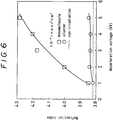
- Fig. 6 illustrates the relationship between the index of refraction and acceleration voltage for the silicon substrate irradiated with CO2 cluster and CO2 monomolecular ions.
- the index of refraction increases with the increase in the acceleration voltage, and the surface is in the non-crystalline state by the ion irradiation.
- the index of refraction is substantially constant for an acceleration voltage of up to 4 kV.
- the value hereof is of the same order as that of a silicon substrate not irradiated, and the damage by irradiation is very slight.
- the area of a peak near the 280th channel suggests that, in the case of irradiation of CO2 cluster ions, the number of damaged silicon atoms is of the order of the area of peak of the non-irradiated silicon substrate, thus showing that the damage caused by ion irradiation is slight.
- the energy input per molecule of cluster which is approximately 6 cV, is far smaller than the energy input per molecule of 3 keV.
- the results presented above teach that, by using cluster ions, it is possible to decrease the energy imparted to the substrate surface to the energy necessary for displacing the surface atoms, thus causing no defects on the substrate surface. Since, furthermore, the adsorption energy of impurity atoms and oxides adsorbed onto the substrate surface is up to several eV, impurities and oxides adsorbed onto the substrate surface are removed by sputtering from the surface. Fluorine and chlorine, which are chemically active, are effective for removing oxides and the like from the solid surface without the necessity of heating, in cooperation with the dynamic energy possessed by the individual atoms.
- the cluster ions may be as required irradiated onto the substrate surface after mass separation by the use of an electric field or a magnetic field.
Landscapes
- Chemical & Material Sciences (AREA)
- Chemical Kinetics & Catalysis (AREA)
- Engineering & Computer Science (AREA)
- Materials Engineering (AREA)
- Mechanical Engineering (AREA)
- Metallurgy (AREA)
- Organic Chemistry (AREA)
- Physical Deposition Of Substances That Are Components Of Semiconductor Devices (AREA)
- Physical Vapour Deposition (AREA)
- ing And Chemical Polishing (AREA)
- Electron Sources, Ion Sources (AREA)
- Chemical Vapour Deposition (AREA)
- Cleaning Or Drying Semiconductors (AREA)
Applications Claiming Priority (2)
| Application Number | Priority Date | Filing Date | Title |
|---|---|---|---|
| JP129512/91 | 1991-05-31 | ||
| JP3129512A JP2662321B2 (ja) | 1991-05-31 | 1991-05-31 | 超低速クラスターイオンビームによる表面処理方法 |
Publications (2)
| Publication Number | Publication Date |
|---|---|
| EP0516480A2 true EP0516480A2 (de) | 1992-12-02 |
| EP0516480A3 EP0516480A3 (en) | 1993-02-03 |
Family
ID=15011330
Family Applications (1)
| Application Number | Title | Priority Date | Filing Date |
|---|---|---|---|
| EP19920304964 Ceased EP0516480A3 (en) | 1991-05-31 | 1992-05-29 | Method for surface treatment with extra-low-speed ion beam |
Country Status (3)
| Country | Link |
|---|---|
| US (1) | US5459326A (de) |
| EP (1) | EP0516480A3 (de) |
| JP (1) | JP2662321B2 (de) |
Cited By (4)
| Publication number | Priority date | Publication date | Assignee | Title |
|---|---|---|---|---|
| US5496506A (en) * | 1992-09-21 | 1996-03-05 | Sony Corporation | Process for removing fine particles |
| FR2793264A1 (fr) * | 1999-05-07 | 2000-11-10 | X Ion | Procede de nettoyage d'une surface de substrat de silicium et application a la fabrication de composants electroniques integres |
| WO2001006538A1 (en) * | 1999-07-19 | 2001-01-25 | Epion Corporation | Adaptive gcib for smoothing surfaces |
| EP1229575A3 (de) * | 2001-02-05 | 2002-08-21 | Speedfam Co., Ltd. | Verfahren zum Entfernen von Nanotopographie |
Families Citing this family (53)
| Publication number | Priority date | Publication date | Assignee | Title |
|---|---|---|---|---|
| JP3352842B2 (ja) * | 1994-09-06 | 2002-12-03 | 科学技術振興事業団 | ガスクラスターイオンビームによる薄膜形成方法 |
| JP3318186B2 (ja) | 1995-05-19 | 2002-08-26 | 科学技術振興事業団 | ガスクラスターの形成方法と薄膜形成方法 |
| US6251835B1 (en) * | 1997-05-08 | 2001-06-26 | Epion Corporation | Surface planarization of high temperature superconductors |
| US6689284B1 (en) * | 1999-09-29 | 2004-02-10 | Kabushiki Kaisha Toshiba | Surface treating method |
| KR100349948B1 (ko) | 1999-11-17 | 2002-08-22 | 주식회사 다산 씨.앤드.아이 | 클러스터를 이용한 건식 세정 장치 및 방법 |
| US6416820B1 (en) | 1999-11-19 | 2002-07-09 | Epion Corporation | Method for forming carbonaceous hard film |
| US6635883B2 (en) | 1999-12-06 | 2003-10-21 | Epion Corporation | Gas cluster ion beam low mass ion filter |
| US6613240B2 (en) | 1999-12-06 | 2003-09-02 | Epion Corporation | Method and apparatus for smoothing thin conductive films by gas cluster ion beam |
| US6331227B1 (en) | 1999-12-14 | 2001-12-18 | Epion Corporation | Enhanced etching/smoothing of dielectric surfaces |
| JP2003527614A (ja) | 2000-03-20 | 2003-09-16 | エピオン コーポレイション | クラスターサイズ測定器具およびクラスターイオンビーム診断方法 |
| US6498107B1 (en) | 2000-05-01 | 2002-12-24 | Epion Corporation | Interface control for film deposition by gas-cluster ion-beam processing |
| US6750460B2 (en) | 2000-05-02 | 2004-06-15 | Epion Corporation | System and method for adjusting the properties of a device by GCIB processing |
| WO2002004696A1 (en) | 2000-07-10 | 2002-01-17 | Epion Corporation | Improving effectiveness of artificial hip by gcib |
| JP2004507037A (ja) | 2000-07-14 | 2004-03-04 | エピオン コーポレイション | Gcibのサイズ診断、及びワークピース加工 |
| EP1348227B1 (de) * | 2000-12-26 | 2006-08-16 | Epion Corporation | Ladungskontroll- und dosimetriesystem sowie verfahren für einen gas-cluster-ionenstrahl |
| EP1392200B1 (de) | 2001-05-09 | 2011-10-12 | Exogenesis Corporation | Verfahren zur verbesserung der effizienz künstlicher gelenke durch anwendung der gascluster-ionenstrahl-technologie |
| US7666462B2 (en) * | 2001-05-11 | 2010-02-23 | Exogenesis Corporation | Method of controlling a drug release rate |
| US7923055B2 (en) | 2001-05-11 | 2011-04-12 | Exogenesis Corporation | Method of manufacturing a drug delivery system |
| US8889169B2 (en) * | 2001-05-11 | 2014-11-18 | Exogenesis Corporation | Drug delivery system and method of manufacturing thereof |
| US7105199B2 (en) * | 2001-05-11 | 2006-09-12 | Exogenesis Corporation | Methods of adhering drugs to the surface of medical devices through ion beam surface modification |
| US7064927B2 (en) * | 2002-05-13 | 2006-06-20 | Hitachi Global Storage Technologies Netherlands B.V. | Disk, method for making it free of asperities utilizing a step of exposing a surface of the disk to a gas cluster ion beam and disk drive unit for using the disk |
| US20030224620A1 (en) * | 2002-05-31 | 2003-12-04 | Kools Jacques C.S. | Method and apparatus for smoothing surfaces on an atomic scale |
| US20040060899A1 (en) * | 2002-10-01 | 2004-04-01 | Applied Materials, Inc. | Apparatuses and methods for treating a silicon film |
| US6833322B2 (en) * | 2002-10-17 | 2004-12-21 | Applied Materials, Inc. | Apparatuses and methods for depositing an oxide film |
| WO2004053945A2 (en) * | 2002-12-12 | 2004-06-24 | Epion Corporation | Re-crystallization of semiconductor surface film and doping of semiconductor by energetic cluster irradiation |
| US20040137158A1 (en) * | 2003-01-15 | 2004-07-15 | Kools Jacques Constant Stefan | Method for preparing a noble metal surface |
| US7405394B2 (en) | 2004-08-24 | 2008-07-29 | Hitachi, Ltd. | Gas cluster-ion irradiation apparatus |
| CN101563760B (zh) | 2006-10-30 | 2011-12-21 | 日本航空电子工业株式会社 | 利用气体团簇离子束的固体表面平坦化方法及固体表面平坦化设备 |
| US8003498B2 (en) * | 2007-11-13 | 2011-08-23 | Varian Semiconductor Equipment Associates, Inc. | Particle beam assisted modification of thin film materials |
| US20090198264A1 (en) * | 2008-01-31 | 2009-08-06 | Exogenesis Corporation | Method and System for Improving Surgical Blades by the Application of Gas Cluster Ion Beam Technology and Improved Surgical Blades |
| US8530859B2 (en) * | 2008-06-26 | 2013-09-10 | Exogenesis Corporation | Method and system for sterilizing objects by the application of gas-cluster ion-beam technology |
| JP2011530347A (ja) * | 2008-08-07 | 2011-12-22 | エクソジェネシス コーポレーション | 薬物送達システムおよびその薬物送達システムの製造方法 |
| EP2326356B1 (de) * | 2008-08-07 | 2017-10-11 | Exogenesis Corporation | Medizinische vorrichtung für knochenimplantat und verfahren zur herstellung einer derartigen vorrichtung |
| JP2010070788A (ja) * | 2008-09-17 | 2010-04-02 | Tokyo Electron Ltd | 基板処理方法 |
| US7785978B2 (en) * | 2009-02-04 | 2010-08-31 | Micron Technology, Inc. | Method of forming memory cell using gas cluster ion beams |
| US8981322B2 (en) * | 2009-02-04 | 2015-03-17 | Tel Epion Inc. | Multiple nozzle gas cluster ion beam system |
| US7982196B2 (en) | 2009-03-31 | 2011-07-19 | Tel Epion Inc. | Method for modifying a material layer using gas cluster ion beam processing |
| US8877299B2 (en) * | 2009-03-31 | 2014-11-04 | Tel Epion Inc. | Method for enhancing a substrate using gas cluster ion beam processing |
| US20100243913A1 (en) * | 2009-03-31 | 2010-09-30 | Tel Epion Inc. | Pre-aligned nozzle/skimmer |
| CN101559627B (zh) * | 2009-05-25 | 2011-12-14 | 天津大学 | 粒子束辅助单晶脆性材料超精密加工方法 |
| US20110039034A1 (en) | 2009-08-11 | 2011-02-17 | Helen Maynard | Pulsed deposition and recrystallization and tandem solar cell design utilizing crystallized/amorphous material |
| JP6278591B2 (ja) | 2012-11-13 | 2018-02-14 | 株式会社Sumco | 半導体エピタキシャルウェーハの製造方法、半導体エピタキシャルウェーハ、および固体撮像素子の製造方法 |
| JP2015138667A (ja) | 2014-01-22 | 2015-07-30 | アルバック・ファイ株式会社 | イオン源、イオン銃、分析装置 |
| US9540725B2 (en) | 2014-05-14 | 2017-01-10 | Tel Epion Inc. | Method and apparatus for beam deflection in a gas cluster ion beam system |
| JP6566683B2 (ja) * | 2014-07-02 | 2019-08-28 | 東京エレクトロン株式会社 | 基板洗浄方法および基板洗浄装置 |
| JP6539959B2 (ja) * | 2014-08-28 | 2019-07-10 | 株式会社Sumco | エピタキシャルシリコンウェーハおよびその製造方法、ならびに、固体撮像素子の製造方法 |
| KR102347960B1 (ko) | 2015-02-03 | 2022-01-05 | 삼성전자주식회사 | 도전체 및 그 제조 방법 |
| JP6545053B2 (ja) | 2015-03-30 | 2019-07-17 | 東京エレクトロン株式会社 | 処理装置および処理方法、ならびにガスクラスター発生装置および発生方法 |
| WO2016158054A1 (ja) | 2015-03-30 | 2016-10-06 | 東京エレクトロン株式会社 | 処理装置および処理方法、ならびにガスクラスター発生装置および発生方法 |
| JP6459948B2 (ja) | 2015-12-15 | 2019-01-30 | 株式会社Sumco | 半導体エピタキシャルウェーハの製造方法および固体撮像素子の製造方法 |
| JP7179661B2 (ja) | 2019-03-27 | 2022-11-29 | アルバック・ファイ株式会社 | ガスクラスターイオンビーム装置、分析装置 |
| US11450506B2 (en) * | 2020-04-24 | 2022-09-20 | Tel Manufacturing And Engineering Of America, Inc. | Pattern enhancement using a gas cluster ion beam |
| CN115304022B (zh) * | 2022-07-07 | 2024-05-24 | 武汉大学 | 基于超低能团簇离子束自组装制备功能纳米结构的方法 |
Family Cites Families (13)
| Publication number | Priority date | Publication date | Assignee | Title |
|---|---|---|---|---|
| JPS50105550A (de) * | 1973-12-11 | 1975-08-20 | ||
| US4217855A (en) * | 1974-10-23 | 1980-08-19 | Futaba Denshi Kogyo K.K. | Vaporized-metal cluster ion source and ionized-cluster beam deposition device |
| JPS521399A (en) * | 1975-06-24 | 1977-01-07 | Toshiba Corp | The fixation treatment method of a radioactive gas and its device |
| US4559096A (en) * | 1984-06-25 | 1985-12-17 | The United States Of America As Represented By The United States Department Of Energy | Method of precisely modifying predetermined surface layers of a workpiece by cluster ion impact therewith |
| US4880687A (en) * | 1986-05-09 | 1989-11-14 | Tdk Corporation | Magnetic recording medium |
| WO1988002790A1 (en) * | 1986-10-15 | 1988-04-21 | Hughes Aircraft Company | Process and apparatus for film deposition utilizing volatile clusters |
| CN1019513B (zh) * | 1986-10-29 | 1992-12-16 | 三菱电机株式会社 | 化合物薄膜形成装置 |
| US4740267A (en) * | 1987-02-20 | 1988-04-26 | Hughes Aircraft Company | Energy intensive surface reactions using a cluster beam |
| US4902572A (en) * | 1988-04-19 | 1990-02-20 | The Boeing Company | Film deposition system |
| US5019712A (en) * | 1989-06-08 | 1991-05-28 | Hughes Aircraft Company | Production of focused ion cluster beams |
| JP2639158B2 (ja) * | 1989-08-02 | 1997-08-06 | 日本電気株式会社 | エッチング方法およびエッチング装置 |
| US5118950A (en) * | 1989-12-29 | 1992-06-02 | The United States Of America As Represented By The Secretary Of The Air Force | Cluster ion synthesis and confinement in hybrid ion trap arrays |
| US5196102A (en) * | 1991-08-08 | 1993-03-23 | Microelectronics And Computer Technology Corporation | Method and apparatus for applying a compound of a metal and a gas onto a surface |
-
1991
- 1991-05-31 JP JP3129512A patent/JP2662321B2/ja not_active Expired - Lifetime
-
1992
- 1992-05-29 EP EP19920304964 patent/EP0516480A3/en not_active Ceased
-
1995
- 1995-01-09 US US08/370,221 patent/US5459326A/en not_active Expired - Lifetime
Cited By (8)
| Publication number | Priority date | Publication date | Assignee | Title |
|---|---|---|---|---|
| US5496506A (en) * | 1992-09-21 | 1996-03-05 | Sony Corporation | Process for removing fine particles |
| US5628954A (en) * | 1992-09-21 | 1997-05-13 | Sony Corporation | Process for detecting fine particles |
| FR2793264A1 (fr) * | 1999-05-07 | 2000-11-10 | X Ion | Procede de nettoyage d'une surface de substrat de silicium et application a la fabrication de composants electroniques integres |
| WO2000068984A1 (fr) * | 1999-05-07 | 2000-11-16 | X-Ion | Procede de nettoyage d'une surface de substrat de silicium et application a la fabrication de composants electroniques integres |
| WO2001006538A1 (en) * | 1999-07-19 | 2001-01-25 | Epion Corporation | Adaptive gcib for smoothing surfaces |
| US6375790B1 (en) | 1999-07-19 | 2002-04-23 | Epion Corporation | Adaptive GCIB for smoothing surfaces |
| EP1229575A3 (de) * | 2001-02-05 | 2002-08-21 | Speedfam Co., Ltd. | Verfahren zum Entfernen von Nanotopographie |
| US6875701B2 (en) | 2001-02-05 | 2005-04-05 | Speedfam Co., Ltd. | Nanotopography removing method |
Also Published As
| Publication number | Publication date |
|---|---|
| EP0516480A3 (en) | 1993-02-03 |
| US5459326A (en) | 1995-10-17 |
| JPH04354865A (ja) | 1992-12-09 |
| JP2662321B2 (ja) | 1997-10-08 |
Similar Documents
| Publication | Publication Date | Title |
|---|---|---|
| US5459326A (en) | Method for surface treatment with extra-low-speed ion beam | |
| US5814194A (en) | Substrate surface treatment method | |
| JP4902088B2 (ja) | ガスクラスターイオンビーム処理による薄膜を改良するためのシステムおよび方法 | |
| US7626183B2 (en) | Methods for modifying features of a workpiece using a gas cluster ion beam | |
| US8691103B2 (en) | Surface profile adjustment using gas cluster ion beam processing | |
| US20110266466A1 (en) | Method for modifying a material layer using gas cluster ion beam processing | |
| US8455060B2 (en) | Method for depositing hydrogenated diamond-like carbon films using a gas cluster ion beam | |
| US4222838A (en) | Method for controlling plasma etching rates | |
| US20100200774A1 (en) | Multi-sequence film deposition and growth using gas cluster ion beam processing | |
| US4981568A (en) | Apparatus and method for producing high purity diamond films at low temperatures | |
| EP0020935A1 (de) | Gasätzverfahren und Vorrichtung, in der feste Maskiermaterialien zur Veränderung der Ätzgeschwindigkeit Verwendung finden | |
| US10670960B2 (en) | Enhanced high aspect ratio etch performance using accelerated neutral beams derived from gas-cluster ion beams | |
| JPS6173332A (ja) | 光処理装置 | |
| Lin et al. | A review of material surface processing utilizing gas cluster ion beam technology | |
| GB1585558A (en) | Growing native semiconductor oxide layers | |
| Taniguchi et al. | Focused-ion-beam-assisted etching of diamond in XeF 2 | |
| JPS6136589B2 (de) | ||
| JPH1012597A (ja) | プラズマエッチング装置及びプラズマエッチング方法 | |
| JPH03163825A (ja) | エッチング方法およびエッチング装置 | |
| US6099698A (en) | Magnetic disc and method of manufacturing same | |
| DE69033151T2 (de) | Ätzverfahren für Verbindungshalbleiter | |
| JPS6044825B2 (ja) | エツチング方法 | |
| US20070010095A1 (en) | Surface treatment method using ion beam and surface treating device | |
| US6468598B1 (en) | Magnetic disk and method of making thereof | |
| RU2003201C1 (ru) | Способ плазмохимического травлени поверхности твердого тела |
Legal Events
| Date | Code | Title | Description |
|---|---|---|---|
| PUAI | Public reference made under article 153(3) epc to a published international application that has entered the european phase |
Free format text: ORIGINAL CODE: 0009012 |
|
| AK | Designated contracting states |
Kind code of ref document: A2 Designated state(s): DE FR GB IT |
|
| PUAL | Search report despatched |
Free format text: ORIGINAL CODE: 0009013 |
|
| AK | Designated contracting states |
Kind code of ref document: A3 Designated state(s): DE FR GB IT |
|
| 17P | Request for examination filed |
Effective date: 19930723 |
|
| 17Q | First examination report despatched |
Effective date: 19950621 |
|
| APAB | Appeal dossier modified |
Free format text: ORIGINAL CODE: EPIDOS NOAPE |
|
| APAB | Appeal dossier modified |
Free format text: ORIGINAL CODE: EPIDOS NOAPE |
|
| APAD | Appeal reference recorded |
Free format text: ORIGINAL CODE: EPIDOS REFNE |
|
| APAB | Appeal dossier modified |
Free format text: ORIGINAL CODE: EPIDOS NOAPE |
|
| APAB | Appeal dossier modified |
Free format text: ORIGINAL CODE: EPIDOS NOAPE |
|
| APBN | Date of receipt of notice of appeal recorded |
Free format text: ORIGINAL CODE: EPIDOSNNOA2E |
|
| STAA | Information on the status of an ep patent application or granted ep patent |
Free format text: STATUS: THE APPLICATION HAS BEEN REFUSED |
|
| 18R | Application refused |
Effective date: 20030613 |
|
| APAF | Appeal reference modified |
Free format text: ORIGINAL CODE: EPIDOSCREFNE |