EP0518059A1 - Herstellung von optischen LiNbO3-Kanalwellenleitern - Google Patents
Herstellung von optischen LiNbO3-Kanalwellenleitern Download PDFInfo
- Publication number
- EP0518059A1 EP0518059A1 EP92107895A EP92107895A EP0518059A1 EP 0518059 A1 EP0518059 A1 EP 0518059A1 EP 92107895 A EP92107895 A EP 92107895A EP 92107895 A EP92107895 A EP 92107895A EP 0518059 A1 EP0518059 A1 EP 0518059A1
- Authority
- EP
- European Patent Office
- Prior art keywords
- optical
- proton exchange
- manufacturing process
- manufacturing
- guides
- Prior art date
- Legal status (The legal status is an assumption and is not a legal conclusion. Google has not performed a legal analysis and makes no representation as to the accuracy of the status listed.)
- Granted
Links
- 230000003287 optical effect Effects 0.000 title claims abstract description 34
- 238000004519 manufacturing process Methods 0.000 title claims abstract description 16
- 229910003327 LiNbO3 Inorganic materials 0.000 title claims abstract description 6
- 238000000034 method Methods 0.000 claims abstract description 15
- 230000008569 process Effects 0.000 claims abstract description 13
- 230000008021 deposition Effects 0.000 claims abstract description 7
- 229910052751 metal Inorganic materials 0.000 claims abstract description 7
- 239000002184 metal Substances 0.000 claims abstract description 7
- WPYMKLBDIGXBTP-UHFFFAOYSA-N benzoic acid Chemical compound OC(=O)C1=CC=CC=C1 WPYMKLBDIGXBTP-UHFFFAOYSA-N 0.000 claims abstract description 6
- 239000005711 Benzoic acid Substances 0.000 claims abstract description 3
- 235000010233 benzoic acid Nutrition 0.000 claims abstract description 3
- 229940031993 lithium benzoate Drugs 0.000 claims abstract description 3
- LDJNSLOKTFFLSL-UHFFFAOYSA-M lithium;benzoate Chemical compound [Li+].[O-]C(=O)C1=CC=CC=C1 LDJNSLOKTFFLSL-UHFFFAOYSA-M 0.000 claims abstract description 3
- VYPSYNLAJGMNEJ-UHFFFAOYSA-N Silicium dioxide Chemical compound O=[Si]=O VYPSYNLAJGMNEJ-UHFFFAOYSA-N 0.000 claims description 18
- 235000012239 silicon dioxide Nutrition 0.000 claims description 9
- 239000000377 silicon dioxide Substances 0.000 claims description 9
- 239000013078 crystal Substances 0.000 claims description 6
- 238000000151 deposition Methods 0.000 claims description 6
- 230000005855 radiation Effects 0.000 claims description 5
- CSCPPACGZOOCGX-UHFFFAOYSA-N Acetone Chemical compound CC(C)=O CSCPPACGZOOCGX-UHFFFAOYSA-N 0.000 claims description 4
- XKRFYHLGVUSROY-UHFFFAOYSA-N Argon Chemical compound [Ar] XKRFYHLGVUSROY-UHFFFAOYSA-N 0.000 claims description 4
- 229920000642 polymer Polymers 0.000 claims description 4
- 238000007669 thermal treatment Methods 0.000 claims description 3
- 229910052786 argon Inorganic materials 0.000 claims description 2
- 238000007654 immersion Methods 0.000 claims description 2
- 238000001755 magnetron sputter deposition Methods 0.000 claims description 2
- 229920003229 poly(methyl methacrylate) Polymers 0.000 claims description 2
- 239000004926 polymethyl methacrylate Substances 0.000 claims description 2
- 229910052681 coesite Inorganic materials 0.000 claims 2
- 229910052906 cristobalite Inorganic materials 0.000 claims 2
- 229910052682 stishovite Inorganic materials 0.000 claims 2
- 229910052905 tridymite Inorganic materials 0.000 claims 2
- 230000001590 oxidative effect Effects 0.000 claims 1
- 238000005516 engineering process Methods 0.000 abstract description 2
- 238000005382 thermal cycling Methods 0.000 abstract 1
- 239000010408 film Substances 0.000 description 12
- RTAQQCXQSZGOHL-UHFFFAOYSA-N Titanium Chemical compound [Ti] RTAQQCXQSZGOHL-UHFFFAOYSA-N 0.000 description 3
- GQYHUHYESMUTHG-UHFFFAOYSA-N lithium niobate Chemical compound [Li+].[O-][Nb](=O)=O GQYHUHYESMUTHG-UHFFFAOYSA-N 0.000 description 3
- 239000010936 titanium Substances 0.000 description 3
- 229910052719 titanium Inorganic materials 0.000 description 3
- 238000010586 diagram Methods 0.000 description 2
- 238000009792 diffusion process Methods 0.000 description 2
- 230000008030 elimination Effects 0.000 description 2
- 238000003379 elimination reaction Methods 0.000 description 2
- 238000002955 isolation Methods 0.000 description 2
- 239000000463 material Substances 0.000 description 2
- 230000005693 optoelectronics Effects 0.000 description 2
- NIXOWILDQLNWCW-UHFFFAOYSA-M Acrylate Chemical compound [O-]C(=O)C=C NIXOWILDQLNWCW-UHFFFAOYSA-M 0.000 description 1
- WHXSMMKQMYFTQS-UHFFFAOYSA-N Lithium Chemical group [Li] WHXSMMKQMYFTQS-UHFFFAOYSA-N 0.000 description 1
- 239000002253 acid Substances 0.000 description 1
- 230000009471 action Effects 0.000 description 1
- 230000008878 coupling Effects 0.000 description 1
- 238000010168 coupling process Methods 0.000 description 1
- 238000005859 coupling reaction Methods 0.000 description 1
- 230000000694 effects Effects 0.000 description 1
- 230000005684 electric field Effects 0.000 description 1
- 239000000835 fiber Substances 0.000 description 1
- 230000004048 modification Effects 0.000 description 1
- 238000012986 modification Methods 0.000 description 1
- 239000013307 optical fiber Substances 0.000 description 1
- 238000001259 photo etching Methods 0.000 description 1
- 239000002904 solvent Substances 0.000 description 1
- 239000000758 substrate Substances 0.000 description 1
- 239000010409 thin film Substances 0.000 description 1
Images

Classifications
-
- G—PHYSICS
- G02—OPTICS
- G02B—OPTICAL ELEMENTS, SYSTEMS OR APPARATUS
- G02B6/00—Light guides; Structural details of arrangements comprising light guides and other optical elements, e.g. couplings
- G02B6/10—Light guides; Structural details of arrangements comprising light guides and other optical elements, e.g. couplings of the optical waveguide type
- G02B6/12—Light guides; Structural details of arrangements comprising light guides and other optical elements, e.g. couplings of the optical waveguide type of the integrated circuit kind
- G02B6/13—Integrated optical circuits characterised by the manufacturing method
- G02B6/134—Integrated optical circuits characterised by the manufacturing method by substitution by dopant atoms
- G02B6/1345—Integrated optical circuits characterised by the manufacturing method by substitution by dopant atoms using ion exchange
-
- G—PHYSICS
- G02—OPTICS
- G02B—OPTICAL ELEMENTS, SYSTEMS OR APPARATUS
- G02B6/00—Light guides; Structural details of arrangements comprising light guides and other optical elements, e.g. couplings
- G02B6/10—Light guides; Structural details of arrangements comprising light guides and other optical elements, e.g. couplings of the optical waveguide type
- G02B6/12—Light guides; Structural details of arrangements comprising light guides and other optical elements, e.g. couplings of the optical waveguide type of the integrated circuit kind
- G02B2006/12035—Materials
- G02B2006/1204—Lithium niobate (LiNbO3)
-
- G—PHYSICS
- G02—OPTICS
- G02B—OPTICAL ELEMENTS, SYSTEMS OR APPARATUS
- G02B6/00—Light guides; Structural details of arrangements comprising light guides and other optical elements, e.g. couplings
- G02B6/10—Light guides; Structural details of arrangements comprising light guides and other optical elements, e.g. couplings of the optical waveguide type
- G02B6/12—Light guides; Structural details of arrangements comprising light guides and other optical elements, e.g. couplings of the optical waveguide type of the integrated circuit kind
- G02B2006/12166—Manufacturing methods
- G02B2006/12169—Annealing
Definitions
- This invention regards a new manufacturing process of Lithium Niobate channel optical guides, obtained in particular on its 'X' cut suface, where a thin dielectric film, within which the channel is defined by photo etching, is used as a template while manufacturing the optical guide and as an insulating film between this guide and the metal electrodes, resulting in a self-aligning process.
- This process pertains to the field of planar integrated optical componenent technologies and it can be advantageously applied to the manufacturing of components used for optical fibre sensors (Reference #1:W.C.Gross et al, Applied Optics, Vol 19,#6, page 852-858, 1980) and for wide band microwave signal processing (Reference #3:T.Sueta and M.Izutsu, IEEE Trans.on Microwave Theory and Techniques, Vol.38,#5, page 477-482, May 1990).
- LiNbO3 channel optical guides more often adopted at present consists of the diffusion of Titanium into the Lithium Niobate crystal (Ref #6: W.K.Burns et al, J.Appl.Phis.,vol.50,#10, pag.6175-6182,October 1979) and of the following deposition of a dielectric film followed by the deposition and definition of the metal electrodes.
- This process is costly in terms of deposition and definition of the Titanium film (complex high accuracy equipment required to determine the thickness of the film) and of the following thermal diffusion of Titanium into the crystal (temperature control at about 1000 deg C).
- a template in the proton exchange process which consists of a dielectric film which is deposited onto the surface and which carries the optical guide channel and also by the thermal tratment which follows the exchance phase.
- the use of a dielectric film covers with one action both the function of proton exchange template and the provision of an insulating layer between the optical guide and the metal electrodes which are later implemented.
- the resulting isolation layer is not present above the optical guide, so as to eliminate the causes of instability of the electro-optical characteristics of the modulator.
- Figure 1 shows a schematic outline of the manufacturing process phases where we can see:
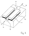
- Figure 2 is a diagram of the structure of the modulator where we can see:
- the optical guide is self aligned with a channel defined in a dielectric layer which is used as an isolation layer between it and the elctrodes of a generic modulator which is shown as an elementary structure in Figure 2.
Landscapes
- Physics & Mathematics (AREA)
- Engineering & Computer Science (AREA)
- Microelectronics & Electronic Packaging (AREA)
- General Physics & Mathematics (AREA)
- Optics & Photonics (AREA)
- Optical Integrated Circuits (AREA)
Applications Claiming Priority (2)
| Application Number | Priority Date | Filing Date | Title |
|---|---|---|---|
| ITRM910316 | 1991-05-10 | ||
| ITRM910316A IT1245961B (it) | 1991-05-10 | 1991-05-10 | Processo di fabbricazione di guide ottiche a canale in linbo3. |
Publications (2)
| Publication Number | Publication Date |
|---|---|
| EP0518059A1 true EP0518059A1 (de) | 1992-12-16 |
| EP0518059B1 EP0518059B1 (de) | 2000-02-16 |
Family
ID=11400136
Family Applications (1)
| Application Number | Title | Priority Date | Filing Date |
|---|---|---|---|
| EP92107895A Expired - Lifetime EP0518059B1 (de) | 1991-05-10 | 1992-05-09 | Herstellung von optischen LiNbO3-Kanalwellenleitern |
Country Status (5)
| Country | Link |
|---|---|
| US (1) | US5356523A (de) |
| EP (1) | EP0518059B1 (de) |
| DE (1) | DE69230680T2 (de) |
| ES (1) | ES2143981T3 (de) |
| IT (1) | IT1245961B (de) |
Cited By (3)
| Publication number | Priority date | Publication date | Assignee | Title |
|---|---|---|---|---|
| WO1995014250A1 (de) * | 1993-11-18 | 1995-05-26 | Forschungszentrum Jülich GmbH | Verfahren zur herstellung einer schichtstruktur und seine verwendung |
| ES2188360A1 (es) * | 2001-03-07 | 2003-06-16 | Univ Catalunya Politecnica | Modulador de fase electrooptico autooscilante. |
| CN112130253A (zh) * | 2020-09-08 | 2020-12-25 | 派尼尔科技(天津)有限公司 | 一种在z切铌酸锂薄膜上制作y传脊型光波导的方法 |
Families Citing this family (3)
| Publication number | Priority date | Publication date | Assignee | Title |
|---|---|---|---|---|
| JP2555942B2 (ja) * | 1993-08-27 | 1996-11-20 | 日本電気株式会社 | 光制御デバイス |
| EP1645361A1 (de) | 2004-10-11 | 2006-04-12 | Knoll Maschinenbau Gmbh | Schneidvorrichtung zum Zerkleinern von Spänen |
| CN100510814C (zh) * | 2007-12-29 | 2009-07-08 | 上海亨通光电科技有限公司 | 高温质子交换的LiNbO3光波导制造方法 |
Citations (2)
| Publication number | Priority date | Publication date | Assignee | Title |
|---|---|---|---|---|
| EP0340983A2 (de) * | 1988-05-03 | 1989-11-08 | AT&T Corp. | Protonenaustauschverfahren zur Herstellung optischer Wellenleiter |
| EP0425076A2 (de) * | 1989-10-27 | 1991-05-02 | Litton Systems, Inc. | Verfahren zur Herstellung von integrierten optischen Chips mit hohen elektro-optischen Koeffizienten |
Family Cites Families (9)
| Publication number | Priority date | Publication date | Assignee | Title |
|---|---|---|---|---|
| US4561718A (en) * | 1983-08-22 | 1985-12-31 | Sperry Corporation | Photoelastic effect optical waveguides |
| DE3417732A1 (de) * | 1984-05-12 | 1986-07-10 | Leybold-Heraeus GmbH, 5000 Köln | Verfahren zum aufbringen von siliziumhaltigen schichten auf substraten durch katodenzerstaeubung und zerstaeubungskatode zur durchfuehrung des verfahrens |
| US4775208A (en) * | 1986-06-06 | 1988-10-04 | Polaroid Corporation | Planar waveguide mode converter device |
| JPS6370203A (ja) * | 1986-09-11 | 1988-03-30 | Brother Ind Ltd | 屈折率分布型光導波路レンズの製造方法 |
| FR2613085B1 (fr) * | 1987-03-25 | 1989-06-09 | Carenco Alain | Procede pour augmenter localement les indices de refraction d'un materiau electro-optique utilisable en optique guidee et materiau obtenu par ce procede |
| JPS6465841A (en) * | 1987-09-07 | 1989-03-13 | Fujitsu Ltd | Formation of pattern |
| KR920005445B1 (ko) * | 1989-08-10 | 1992-07-04 | 한국과학기술원 | 광도파로 제작방법 및 구조 |
| US5018811A (en) * | 1990-07-18 | 1991-05-28 | Northrop Corporation | Asymmetric optical waveguides for minimizing bending losses and techniques for fabricating same |
| US5062688A (en) * | 1990-09-14 | 1991-11-05 | Nippon Sheet Glass Co., Ltd. | Flat plate optical element and method for preparing the same |
-
1991
- 1991-05-10 IT ITRM910316A patent/IT1245961B/it active IP Right Grant
-
1992
- 1992-05-09 DE DE69230680T patent/DE69230680T2/de not_active Expired - Fee Related
- 1992-05-09 EP EP92107895A patent/EP0518059B1/de not_active Expired - Lifetime
- 1992-05-09 ES ES92107895T patent/ES2143981T3/es not_active Expired - Lifetime
- 1992-05-11 US US07/882,146 patent/US5356523A/en not_active Expired - Lifetime
Patent Citations (2)
| Publication number | Priority date | Publication date | Assignee | Title |
|---|---|---|---|---|
| EP0340983A2 (de) * | 1988-05-03 | 1989-11-08 | AT&T Corp. | Protonenaustauschverfahren zur Herstellung optischer Wellenleiter |
| EP0425076A2 (de) * | 1989-10-27 | 1991-05-02 | Litton Systems, Inc. | Verfahren zur Herstellung von integrierten optischen Chips mit hohen elektro-optischen Koeffizienten |
Non-Patent Citations (2)
| Title |
|---|
| IEEE PHOTONICS TECHNOLOGY LETTERS vol. 2, no. 3, March 1990, NEW YORK US pages 184 - 186; Y.-S. SON ET AL.: 'Control of mode profiles in proton-diffused LiNbO3 waveguides using self-aligned SiO2 cladding' * |
| PATENT ABSTRACTS OF JAPAN vol. 11, no. 12 (P-535)(2459) 13 January 1987 & JP-A-61 188 502 ( MATSUSHITA ) 22 August 1986 * |
Cited By (5)
| Publication number | Priority date | Publication date | Assignee | Title |
|---|---|---|---|---|
| WO1995014250A1 (de) * | 1993-11-18 | 1995-05-26 | Forschungszentrum Jülich GmbH | Verfahren zur herstellung einer schichtstruktur und seine verwendung |
| US5882400A (en) * | 1993-11-18 | 1999-03-16 | Forschungszentrum Julich Gmbh | Method of producing a layer structure and the use of the method |
| ES2188360A1 (es) * | 2001-03-07 | 2003-06-16 | Univ Catalunya Politecnica | Modulador de fase electrooptico autooscilante. |
| ES2188360B1 (es) * | 2001-03-07 | 2005-02-16 | Universitat Politecnica De Catalunya | Modulador de fase electrooptico autooscilante. |
| CN112130253A (zh) * | 2020-09-08 | 2020-12-25 | 派尼尔科技(天津)有限公司 | 一种在z切铌酸锂薄膜上制作y传脊型光波导的方法 |
Also Published As
| Publication number | Publication date |
|---|---|
| ITRM910316A0 (it) | 1991-05-10 |
| ITRM910316A1 (it) | 1992-11-10 |
| DE69230680T2 (de) | 2000-08-17 |
| ES2143981T3 (es) | 2000-06-01 |
| IT1245961B (it) | 1994-11-07 |
| DE69230680D1 (de) | 2000-03-23 |
| EP0518059B1 (de) | 2000-02-16 |
| US5356523A (en) | 1994-10-18 |
Similar Documents
| Publication | Publication Date | Title |
|---|---|---|
| US9746743B1 (en) | Electro-optic optical modulator devices and method of fabrication | |
| Mercante et al. | 110 GHz CMOS compatible thin film LiNbO3 modulator on silicon | |
| EP1714317B1 (de) | Optische bauelemente mit dünnen ferroelektrischen filmen | |
| Ghosh et al. | Optical isolator for TE polarized light realized by adhesive bonding of Ce: YIG on silicon-on-insulator waveguide circuits | |
| US5134681A (en) | Integrated optic waveguide and fabrication method | |
| US5502780A (en) | Waveguide type optical device | |
| US6185033B1 (en) | Hybrid integrated electro-optical modulator of the pockels effect type | |
| US5818983A (en) | Optical integrated circuit, optical circuit waveguide device and process for oriented, selective growth and formation of organic film | |
| US6037105A (en) | Optical waveguide device fabricating method | |
| EP0642052A1 (de) | Optische Wellenleiteranordnung aus Polymermaterial mit thermooptischen Eigenschaften | |
| Lee et al. | Optical intensity modulator based on a novel electrooptic polymer incorporating high/spl mu//spl beta/chromophore | |
| US5291574A (en) | Method for manufacturing strip optical waveguides | |
| US4056304A (en) | Light modulation employing single crystal optical waveguides of niobium-doped lithium tantalate | |
| EP0518059A1 (de) | Herstellung von optischen LiNbO3-Kanalwellenleitern | |
| US4733927A (en) | Stress waveguides in bulk crystalline materials | |
| EP1224491B1 (de) | Wellenleiter mit eindiffundiertem titan und zugehöriges herstellungsverfahren | |
| Noguchi et al. | 40-Gbit/s Ti: LiNbO 3 optical modulator with a two-stage electrode | |
| Song et al. | Analysis and demonstration of Mach–Zehnder polymer modulators using in-plane coplanar waveguide structure | |
| EP1078296B1 (de) | Verfahren zum tempern unter druck von lithiumniobat oder lithiumtantalat und so hergestellte lithiumniobat bzw. lithiumtantalat-strukturen | |
| Hamilton et al. | Polymer in-line fiber modulators for broadband radio-frequency optical links | |
| US6786967B1 (en) | Ion exchange waveguides and methods of fabrication | |
| JP2847660B2 (ja) | 導波路型光変調器 | |
| KR0175743B1 (ko) | 비선형 광학 고분자를 이용한 전기적 횡파 모드편광장치 및 그 제조 방법 | |
| JP2868046B2 (ja) | 光変調器 | |
| JP2003202533A (ja) | 有機導波路型光変調器および有機導波路型光変調器の製造方法 |
Legal Events
| Date | Code | Title | Description |
|---|---|---|---|
| PUAI | Public reference made under article 153(3) epc to a published international application that has entered the european phase |
Free format text: ORIGINAL CODE: 0009012 |
|
| AK | Designated contracting states |
Kind code of ref document: A1 Designated state(s): DE ES FR GB NL SE |
|
| 17P | Request for examination filed |
Effective date: 19930605 |
|
| 17Q | First examination report despatched |
Effective date: 19931029 |
|
| GRAG | Despatch of communication of intention to grant |
Free format text: ORIGINAL CODE: EPIDOS AGRA |
|
| GRAG | Despatch of communication of intention to grant |
Free format text: ORIGINAL CODE: EPIDOS AGRA |
|
| RAP1 | Party data changed (applicant data changed or rights of an application transferred) |
Owner name: FINMECCANICA S.P.A. |
|
| RAP1 | Party data changed (applicant data changed or rights of an application transferred) |
Owner name: FINMECCANICA S.P.A. |
|
| GRAG | Despatch of communication of intention to grant |
Free format text: ORIGINAL CODE: EPIDOS AGRA |
|
| GRAH | Despatch of communication of intention to grant a patent |
Free format text: ORIGINAL CODE: EPIDOS IGRA |
|
| RAP1 | Party data changed (applicant data changed or rights of an application transferred) |
Owner name: ALENIA MARCONI SYSTEMS S.P.A. |
|
| GRAH | Despatch of communication of intention to grant a patent |
Free format text: ORIGINAL CODE: EPIDOS IGRA |
|
| GRAA | (expected) grant |
Free format text: ORIGINAL CODE: 0009210 |
|
| AK | Designated contracting states |
Kind code of ref document: B1 Designated state(s): DE ES FR GB NL SE |
|
| REF | Corresponds to: |
Ref document number: 69230680 Country of ref document: DE Date of ref document: 20000323 |
|
| ET | Fr: translation filed | ||
| REG | Reference to a national code |
Ref country code: ES Ref legal event code: FG2A Ref document number: 2143981 Country of ref document: ES Kind code of ref document: T3 |
|
| PLBE | No opposition filed within time limit |
Free format text: ORIGINAL CODE: 0009261 |
|
| STAA | Information on the status of an ep patent application or granted ep patent |
Free format text: STATUS: NO OPPOSITION FILED WITHIN TIME LIMIT |
|
| 26N | No opposition filed | ||
| REG | Reference to a national code |
Ref country code: GB Ref legal event code: IF02 |
|
| PGFP | Annual fee paid to national office [announced via postgrant information from national office to epo] |
Ref country code: ES Payment date: 20070516 Year of fee payment: 16 |
|
| PGFP | Annual fee paid to national office [announced via postgrant information from national office to epo] |
Ref country code: DE Payment date: 20070728 Year of fee payment: 16 |
|
| PGFP | Annual fee paid to national office [announced via postgrant information from national office to epo] |
Ref country code: SE Payment date: 20080529 Year of fee payment: 17 |
|
| PGFP | Annual fee paid to national office [announced via postgrant information from national office to epo] |
Ref country code: GB Payment date: 20080514 Year of fee payment: 17 |
|
| PG25 | Lapsed in a contracting state [announced via postgrant information from national office to epo] |
Ref country code: DE Free format text: LAPSE BECAUSE OF NON-PAYMENT OF DUE FEES Effective date: 20081202 |
|
| REG | Reference to a national code |
Ref country code: ES Ref legal event code: FD2A Effective date: 20080510 |
|
| PGFP | Annual fee paid to national office [announced via postgrant information from national office to epo] |
Ref country code: NL Payment date: 20090528 Year of fee payment: 18 |
|
| PGFP | Annual fee paid to national office [announced via postgrant information from national office to epo] |
Ref country code: FR Payment date: 20090326 Year of fee payment: 18 |
|
| PG25 | Lapsed in a contracting state [announced via postgrant information from national office to epo] |
Ref country code: ES Free format text: LAPSE BECAUSE OF NON-PAYMENT OF DUE FEES Effective date: 20080510 |
|
| GBPC | Gb: european patent ceased through non-payment of renewal fee |
Effective date: 20090509 |
|
| PG25 | Lapsed in a contracting state [announced via postgrant information from national office to epo] |
Ref country code: GB Free format text: LAPSE BECAUSE OF NON-PAYMENT OF DUE FEES Effective date: 20090509 |
|
| REG | Reference to a national code |
Ref country code: NL Ref legal event code: V1 Effective date: 20101201 |
|
| REG | Reference to a national code |
Ref country code: FR Ref legal event code: ST Effective date: 20110131 |
|
| PG25 | Lapsed in a contracting state [announced via postgrant information from national office to epo] |
Ref country code: NL Free format text: LAPSE BECAUSE OF NON-PAYMENT OF DUE FEES Effective date: 20101201 |
|
| PG25 | Lapsed in a contracting state [announced via postgrant information from national office to epo] |
Ref country code: FR Free format text: LAPSE BECAUSE OF NON-PAYMENT OF DUE FEES Effective date: 20100531 Ref country code: SE Free format text: LAPSE BECAUSE OF NON-PAYMENT OF DUE FEES Effective date: 20090510 |