EP0520580B1 - Méthode et appareils pour tester les connexions ATM - Google Patents
Méthode et appareils pour tester les connexions ATM Download PDFInfo
- Publication number
- EP0520580B1 EP0520580B1 EP92201878A EP92201878A EP0520580B1 EP 0520580 B1 EP0520580 B1 EP 0520580B1 EP 92201878 A EP92201878 A EP 92201878A EP 92201878 A EP92201878 A EP 92201878A EP 0520580 B1 EP0520580 B1 EP 0520580B1
- Authority
- EP
- European Patent Office
- Prior art keywords
- cell
- test
- activated
- output signal
- evaluation circuit
- Prior art date
- Legal status (The legal status is an assumption and is not a legal conclusion. Google has not performed a legal analysis and makes no representation as to the accuracy of the status listed.)
- Expired - Lifetime
Links
- 238000012360 testing method Methods 0.000 title claims abstract description 58
- 238000000034 method Methods 0.000 title claims description 15
- 238000011156 evaluation Methods 0.000 claims description 20
- 230000005540 biological transmission Effects 0.000 claims description 4
- 238000012423 maintenance Methods 0.000 claims description 4
- 238000001514 detection method Methods 0.000 claims 1
- 238000012546 transfer Methods 0.000 description 9
- 101100452680 Arabidopsis thaliana INVC gene Proteins 0.000 description 3
- 101001042189 Lens culinaris Bowman-Birk type proteinase inhibitor Proteins 0.000 description 3
- 230000004913 activation Effects 0.000 description 3
- 238000005259 measurement Methods 0.000 description 3
- 238000010586 diagram Methods 0.000 description 2
- 239000000284 extract Substances 0.000 description 2
- 230000006870 function Effects 0.000 description 2
- 230000003213 activating effect Effects 0.000 description 1
- 230000002411 adverse Effects 0.000 description 1
- 230000002457 bidirectional effect Effects 0.000 description 1
- 230000008034 disappearance Effects 0.000 description 1
- 230000000063 preceeding effect Effects 0.000 description 1
- 238000012545 processing Methods 0.000 description 1
- 230000004044 response Effects 0.000 description 1
Images


Classifications
-
- H—ELECTRICITY
- H04—ELECTRIC COMMUNICATION TECHNIQUE
- H04L—TRANSMISSION OF DIGITAL INFORMATION, e.g. TELEGRAPHIC COMMUNICATION
- H04L12/00—Data switching networks
- H04L12/54—Store-and-forward switching systems
-
- H—ELECTRICITY
- H04—ELECTRIC COMMUNICATION TECHNIQUE
- H04L—TRANSMISSION OF DIGITAL INFORMATION, e.g. TELEGRAPHIC COMMUNICATION
- H04L1/00—Arrangements for detecting or preventing errors in the information received
- H04L1/0078—Avoidance of errors by organising the transmitted data in a format specifically designed to deal with errors, e.g. location
- H04L1/0083—Formatting with frames or packets; Protocol or part of protocol for error control
Definitions
- the present invention relates to a method for testing the characteristics of an ATM connection between a first and a second point of an ATM network, to a test cell generator with devices for generating the data sequence of predetermined ATM test cells at said first point and to an evaluation circuit for testing said predetermined ATM test cells at said second point.
- a solution to this problem is given by a method according to claim 1. This method is preferably performed by means of a test cell generator according to claim 4 and of an evaluation circuit according to claim 10.
- a suitably built up test cell just as every ATM cell, comprises a cell header and an information part, the information part according to the invention having twice the same contents, amongst which a time indication, a connection number and a sequence number of the cell in a connection.
- the repetition of the contents happens in inverse form.
- each octet should be followed by its inverse.
- the European Patent Application EP-A2-0 402 741 discloses a method and a device for detecting and correcting errors in the header of any incoming ATM cell.
- this known method is not adapted to test all the above characteristics of an ATM connection.
- the known method does not disclose nor teach the use of specific test cells having a particular layout by which the information part of the test cell is adapted to test these characteristics. It further do also not disclose a test cell generator nor an evaluation circuit adapted to handle such particular test cells.
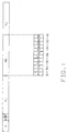
- the first line of Fig. 1 shows the structure of a complete ATM test cell.
- the cell begins with a header H comprising five octets or bytes.
- This cell header H is used in a known way to transfer the cell to a predetermined destination within an ATM network.
- the structure of this cell header is not characteristic for the invention and the cell header may be changed on purpose within the course of a connection. It can therefore not be included in the test.
- the header H for instance contains a pair of bits serving to distinguish test and maintenance cells from data cells within a connection, whereas the first octet MCT of the information part following the cell header H is used to distinguish test cells from maintenance cells.
- MCT a predetermined code has to be reserved.
- the following octet, MCT represents the inverse of the preceeding octet MCT. This inversion is performed in such a way that every bit is inverted.
- MCT and MCT are followed by 18 octets which alternately contain either only ones or zeroes. Each pair of such octets constitutes a flag FL. These 18 octets have three purposes. Errors which maintain a connection continuously on zero or on one should be recognized. Two types of ATM test cells should be distinguished from each other, namely a TYPE-1 cell the data of which are transmitted in a non-inverted way and is followed by their inverse form and a TYPE-0 cell the data of which are inverted, the following inverted octet then containing the non inverted data. Each pair of octets is finally also used to detect bit errors.
- Measurement data MD follow these 18 octets.
- Three different measurement data are transmitted, namely a time indication TS, a sequence number SN of the cell in the connection, and a connection number ID. These three measurement data are each time transmitted as 16-bit words.
- a TYPE-1 cell T1C the transfer is performed in the order T1, T1 , T2, T2 , etc. as represented in Fig. 1.
- the time indication TS is used to take the variation in transfer time (delay time) into account.
- the sequence number SN is used to detect the disappearance or repetition of a cell.
- a faulty connection number ID indicates that a cell of another connection has erroneously appeared in this connection and that the cell header thus has been modified erroneously.
- test cell is completed with octets which again alternately contain only ones or only zeroes.
- octets which again alternately contain only ones or only zeroes.
- Fig. 2 shows an embodiment of a test cell generator by which the above described ATM cells may be generated.
- the test cell generator TG includes a control circuit TCGC, a read and write memory MEM, a connection number generator ID, a clock LT, a three-state bus TSB having a width of 8 bits, an inverter INV and an output register REG.
- the clock circuit LT, the connection number generator ID and the memory MEM are provided with three-state outputs which are able to be activated via activation inputs OE1, OE2, OE3 with the help of the like named activation signals OE1, OE2, OE3.
- the leads of the three-state bus TSB are connected to the supply voltage VCC via resistances R.
- the clock circuit LT and the connection number generator ID are provided with an inverting input SeUL via which and by means of a like named inversion signal SeUL an inversion from high value to low value data bytes and vice-versa may be realized.
- the clock circuit LT is controlled by the cell clock circuit CCL, whilst the output register REG is controlled by the byte clock BCL.
- the inverter INV may be switched between the non inverting and the inverting condition by means of a signal INVC.
- the memory MEM may transmit data via the bus TSB as well as to the control circuit TCGC or receive data from this circuit.
- an 8-bit wide bidirectional data connection MDA is provided between both circuits and between the control circuit TCGC and the memory MEM also a three bit wide address connection, a write lead MW and a read lead MR are foreseen.
- control circuit TCGC is also provided with outputs OE1, OE2, OE3 for the activating signals OE1, OE2 and OE3 and for the activation of the three-state outputs, with an output SeUL for the like named inversion signal SeUL, with outputs CCL and BCL for the cell clock CCL and the byte clock BCL, and with the output INVC for the signal INVC controlling the inverter INV.
- the octets of the cell header H are generated by the memory MEM and fed through the inverter INV without inversion.
- the two following octets, MCT and MCT are generated by the memory MEM two times after each other in the non-inverse form and are fed through the inverter once without inversion and once with inversion.
- the flags FL are formed with the help of the resistances R when the three-state outputs are not activated, and then by alternate non-inversion and inversion in the inverter INV.
- the time indication is provided by the clock circuit LT, the sequence number is generated by the memory MEM and the connection number is provided by the connection number generator ID.
- the subsequent flags are obtained in the same way as the first flags.
- the control circuit TCGC essentially operates in the same way as a known programming circuit, requiring a counter and a programme memory. To these circuits an adder circuit for incrementing the sequence number as well as known devices for providing the timing have to be added.
- Fig. 3 shows a possible embodiment of an evaluation circuit EC for testing ATM test cells.
- This evaluation circuit EC includes a circuit ERRC for fault recognition, a circuit HIDC for e.g. cell header recognition, a circuit TYPD for cell type recognition, a clock LCTI, a circuit SEQE for determining the sequence number, and a circuit DELC for determining a relative or absolute transfer time.
- the fault recognition circuit ERRC investigates if octets occur in associated pairs which are mutually inverted. To this end a memory, an inverter and a comparison circuit are required for each of the eight bits. The errors occurring within an ATM test cell are counted, the counter position of this counter constituting the signal ERR PAT. Further signals are provided: ERR SEQ when an error occurs in the connection number; ERR TIME when an error occurs in the time indication, and ERR ID when an error occurs in the sequence number. The signals ERR PAT and ERR ID are also transmitted to the circuit for cell header recognition HIDC.
- the so called cell header recognition circuit HIDC compares the five bytes of the cell header of an incoming cell with the five bytes of a reference cell, the header bytes each including a pair of above mentioned bits, hereafter called PT, which are activated when test or maintenance cells are concerned and which are not activated in the case of data cells.
- PT the header bytes each including a pair of above mentioned bits
- the circuit for cell type recognition TYPD distinguishes between cells of type TYPE-1 and cells of TYPE-0 and produces a signal TYPE indicating the cell type.
- the circuit SEQE for determining the sequence number extracts the sequence number as a 16-bit signal SEQ NR in function of the signal TYPE.
- the circuit DELC for determining the relative or absolute transfer time DERLC extracts the time indication TS from the cell in function of the signal TYPE, subtracts it from the local time LTI of the clock LCTI and produces at its output the difference as a 16-bit signal DL.
- the clock circuit LT in the test cell generator T6 and the clock LCTI in the evaluation circuit are not running in synchronism the absolute transfer time cannot be obtained.
- the relative transfer time differences may be obtained in this way and these transfer time differences are in general of greater importance than the absolute values of the transfer times.
Landscapes
- Engineering & Computer Science (AREA)
- Computer Networks & Wireless Communication (AREA)
- Signal Processing (AREA)
- Data Exchanges In Wide-Area Networks (AREA)
Claims (19)
- Procédé pour tester les caractéristiques d'une connexion ATM entre un premier et un second point d'un réseau ATM, caractérisé en ce que ledit procédé comprend l'étape consistant à transmettre une séquence de cellules de test prédéterminées audit premier point, et l'étape consistant à recevoir et à tester lesdites cellule de test audit second point, chacune desdites cellules de test comprenant un en-tête et une partie information, ladite partie information comporte deux portions portant les mêmes contenus, la seconde portion étant l'inverse de la première.
- Procédé selon la revendication 1, caractérisé en ce que les deux portions sont entremêlées d'une manière telle que chaque octet de la première portion est suivi immédiatement par l'octet inversé associé de la seconde portion.
- Procédé selon la revendication 1, caractérisé en ce que chaque partie information comprend au moins une indication temporelle du temps de transmission (TS), un numéro de séquence (SN) dans la connexion ATM et un numéro de connexion (ID), ces informations étant sous la forme inverse ou non et en ce que le reste de l'information ne comprenant aucune de ces données contient une indication (FL) que lesdites données sont sous forme inverse ou non.
- Générateur de cellules de test avec des dispositifs pour produire la séquence de données d'une cellule de test ATM prédéterminée à un premier point d'un réseau ATM et selon le procédé de la revendication 1, caractérisé en ce que les dispositifs sont exécutés d'une manière telle que la séquence de données peut sélectivement, et au moins pièce par pièce, être produite sous forme non inversée ou sous forme inversée.
- Générateur de cellules de test selon la revendication 4, caractérisé en ce que la séquence de données est réalisée sous la forme d'octets et est éventuellement inversée par octet.
- Générateur de cellules de test selon la revendication 5, caractérisé en ce que les dispositifs comprennent : un circuit d'horloge (LT) commandé par l'horloge de cellule (CCL), un générateur de numéro de connexion (ID), une mémoire d'écriture et de lecture (MEM), un circuit de commande (TCGC), un inverseur commutable (INV) et un registre de sortie (REG).
- Générateur de cellules de test selon la revendication 6, caractérisé en ce que le circuit d'horloge (LT), le générateur de numéro de connexion (ID) et la mémoire d'écriture et de lecture (MEM) sont tous accouplés au registre de sortie (REG) via un inverseur (INV) et en ce que toutes ces unités sont commandées par le circuit de commande (TCGC).
- Générateur de cellules de test selon la revendication 7, caractérisé en ce qu'il produit des cellules de test dont la partie information comprend au moins : une indication temporelle (TS) du temps d'émission, un numéro de séquence (SN) dans une connexion ATM et un numéro de connexion (ID) fournis par le circuit d'horloge (LT), la mémoire (MEM) et le générateur de numéro de connexion (ID), respectivement.
- Générateur de cellules de test selon la revendication 7, caractérisé en ce que ladite mémoire (MEM) produit aussi les en-têtes des cellules de test.
- Circuit d'évaluation pour tester des cellules de test ATM prédéterminées à un second point d'un réseau ATM et selon le procédé de la revendication 1, caractérisé en ce que ledit circuit d'évaluation comprend un circuit de reconnaissance d'en-tête de cellule (HIDC) qui, en comparant une cellule entrante à une cellule de référence, est à même de trouver si ladite cellule entrante est destinée au circuit d'évaluation (CELL REC) ou non.
- Circuit d'évaluation selon la revendication 10, caractérisé en ce que les données de ladite cellule de test sont inversées octet par octet et en ce qu'on fournit un circuit (TYPD) pour trouver si les données reçues sont tout d'abord non inversée et ensuite inversées ou vice versa.
- Circuit d'évaluation selon la revendication 10, caractérisé en ce que ladite cellule de test comprend une indication temporelle (TS) du temps d'émission et en ce qu'il est prévu un circuit (DELC) destiné à extraire ladite indication temporelle (TS) de ladite cellule de test et à calculer sa différence avec une indication temporelle locale (LCTI).
- Circuit d'évaluation selon la revendication 10, caractérisé en ce que les cellules entrantes audit second point comportent un en-tête (H) avec une première indication de cellule (PT) qui est activée lorsque ladite cellule de test ou une cellule de maintenance et non une cellule de données normale est concernée, et en ce que ces cellules contiennent en outre une partie information comportant une seconde indication de cellule (MCT,
MCT ) qui est activée lorsque ladite cellule de test est concernée, une indication temporelle (TS) du temps d'émission de ladite cellule de test, un numéro de séquence (SN) dans la connexion ATM et un numéro de connexion (ID). - Circuit d'évaluation selon la revendication 13, caractérisé en ce que ledit circuit de reconnaissance d'en-tête de cellule (HIDC) compare l'en-tête d'une cellule entrante à celui de ladite cellule de référence et en ce que, lorsque ces en-têtes sont égaux et que la première indication de cellule (PT) est activée, il compare en outre les secondes indications de cellule (MCT,
MCT ) et dans le cas où elles sont égales fournit un premier signal de sortie (CELL REC) qui indique que la cellule entrante est destinée au circuit d'évaluation. - Circuit d'évaluation selon la revendication 14, caractérisé en ce que ledit premier signal de sortie (CELL REC) est également activé lorsque les en-têtes comparés sont égaux, mais lorsque les premières indications de cellules (PT) ne sont pas activées.
- Circuit d'évaluation selon la revendication 14 ou 15, caractérisé en ce que le circuit de reconnaissance d'en-tête de cellule, lorsque le premier signal de sortie (CELL REC) est activé, compare aussi le numéro de connexion (ID) de la cellule entrante à celui de la cellule de référence et produit un second signal de sortie activé (CELL INS) lorsque ces numéros de connexion sont différents et qu'il n'y a aucune erreur dans le numéro de connexion de la cellule entrante, ledit second signal de sortie activé (CELL INS) indiquant une erreur.
- Circuit d'évaluation selon la revendication 10, caractérisé en ce qu'il comprend un circuit de reconnaissance d'erreurs (ERRC) pour détecter et corriger des erreurs sur les bits, les erreurs détectées étant comptées et le résultat de ce comptage étant indiqué par un troisième signal de sortie (ERR PAT).
- Circuit d'évaluation selon les revendications 13 et 17, caractérisé en ce que ledit circuit de reconnaissance d'erreurs (ERRC) vérifie aussi les erreurs sur les bits dans un numéro de connexion entrant et, lors de la détection d'une erreur, active un quatrième signal de sortie (ERR ID).
- Circuit d'évaluation selon les revendications 16 et 18, caractérisé en ce que le second signal de sortie (CELL INS) est activé lorsque le premier signal de sortie (CELL REC) et le quatrième signal de sortie (ERR ID) sont activés et lorsque le troisième signal de sortie (ERR PAT) dépasse un seuil prédéterminé.
Applications Claiming Priority (2)
| Application Number | Priority Date | Filing Date | Title |
|---|---|---|---|
| BE9100619 | 1991-06-28 | ||
| BE9100619A BE1004959A3 (nl) | 1991-06-28 | 1991-06-28 | Werkwijze en inrichtingen voor het testen van atm-verbindingen. |
Publications (2)
| Publication Number | Publication Date |
|---|---|
| EP0520580A1 EP0520580A1 (fr) | 1992-12-30 |
| EP0520580B1 true EP0520580B1 (fr) | 1998-07-22 |
Family
ID=3885589
Family Applications (1)
| Application Number | Title | Priority Date | Filing Date |
|---|---|---|---|
| EP92201878A Expired - Lifetime EP0520580B1 (fr) | 1991-06-28 | 1992-06-25 | Méthode et appareils pour tester les connexions ATM |
Country Status (11)
| Country | Link |
|---|---|
| US (1) | US5570357A (fr) |
| EP (1) | EP0520580B1 (fr) |
| JP (1) | JPH05191442A (fr) |
| KR (1) | KR0163201B1 (fr) |
| AT (1) | ATE168844T1 (fr) |
| AU (1) | AU1856292A (fr) |
| BE (1) | BE1004959A3 (fr) |
| CA (1) | CA2072516A1 (fr) |
| DE (1) | DE69226313T2 (fr) |
| ES (1) | ES2118785T3 (fr) |
| TW (1) | TW211607B (fr) |
Families Citing this family (13)
| Publication number | Priority date | Publication date | Assignee | Title |
|---|---|---|---|---|
| SE470544B (sv) * | 1992-11-24 | 1994-07-25 | Ellemtel Utvecklings Ab | För en bitfelsövervakning i en väljarutrustning avsedd anordning |
| FR2701618B1 (fr) * | 1993-02-16 | 1995-06-23 | Tremel Jean Yves | Procede de mesure de parametres de performance d'un reseau atm et dispositif de mise en oeuvre. |
| FR2711466B1 (fr) * | 1993-10-20 | 1996-01-26 | Tremel Jean Yves | Appareil de test de réseau de télécommunication de type ATM et de mesure de performance de connexion ATM. |
| JPH07162435A (ja) * | 1993-12-06 | 1995-06-23 | Fujitsu Ltd | 半固定パス確認方法および装置 |
| US5768300A (en) * | 1996-02-22 | 1998-06-16 | Fujitsu Limited | Interconnect fault detection and localization method and apparatus |
| DE19641398A1 (de) * | 1996-09-27 | 1998-04-02 | Siemens Ag | Verfahren zum Ermitteln von auf einer ATM-Übertragungsstrecke in ATM-Nutzzellen aufgetretenen Bitfehlern mit Hilfe von Monitoring-OAM-Zellen |
| DE19641399A1 (de) * | 1996-09-27 | 1998-04-02 | Siemens Ag | Verfahren zum Ermitteln von auf einer ATM-Übertragungsstrecke in ATM-Nutzzellen aufgetretenen Bitfehlern mit Hilfe von Monitoring-OAM-Zellen |
| KR100204061B1 (ko) | 1996-12-21 | 1999-06-15 | 이계철 | 에이티엠 교환시스템에서의 시험기능을 구비한 가입자제어모듈 |
| JP3479248B2 (ja) | 1999-12-17 | 2003-12-15 | 日本電気株式会社 | Atm伝送試験装置 |
| KR100711658B1 (ko) * | 2001-08-28 | 2007-04-27 | 엘지노텔 주식회사 | 에이티엠 네트워크의 중계선 시험 방법 |
| US7355981B2 (en) * | 2001-11-23 | 2008-04-08 | Apparent Networks, Inc. | Signature matching methods and apparatus for performing network diagnostics |
| US8089888B2 (en) * | 2001-12-10 | 2012-01-03 | Qualcomm Incorporated | Method and apparatus for testing traffic and auxiliary channels in a wireless data communication system |
| US7194661B1 (en) * | 2002-12-23 | 2007-03-20 | Intel Corporation | Keep alive buffers (KABs) |
Family Cites Families (12)
| Publication number | Priority date | Publication date | Assignee | Title |
|---|---|---|---|---|
| US4320881A (en) * | 1980-10-03 | 1982-03-23 | American Standard Inc. | Fail-safe decoder for digital track circuits |
| DE3047239C2 (de) * | 1980-12-16 | 1982-12-30 | Wandel & Goltermann Gmbh & Co, 7412 Eningen | Verfahren und Schaltungsanordnung zum Messen der Güte digitaler Übertragungsstrecken und -einrichtungen |
| US4551833A (en) * | 1983-08-10 | 1985-11-05 | At&T Bell Laboratories | Distributed monitoring of packet transmission delay |
| JPS61145799A (ja) * | 1984-12-20 | 1986-07-03 | Fujitsu Ltd | メモリを内蔵した半導体集積回路 |
| US4712214A (en) * | 1986-01-10 | 1987-12-08 | International Business Machines Corporation | Protocol for handling transmission errors over asynchronous communication lines |
| US4939746A (en) * | 1987-06-03 | 1990-07-03 | General Electric Company | Trunked radio repeater system |
| EP0317683B1 (fr) * | 1987-11-27 | 1993-06-30 | International Business Machines Corporation | Les moyens de contrôle de la validité des données |
| DE3912660C1 (fr) * | 1989-04-18 | 1990-08-30 | Wandel & Goltermann Gmbh & Co, 7412 Eningen, De | |
| ATE127986T1 (de) * | 1989-06-16 | 1995-09-15 | Siemens Ag | Verfahren und schaltungsanordnung für das weiterleiten von nach einem asynchronen transfermodus übertragenen zellen. |
| DE4014766A1 (de) * | 1990-04-19 | 1992-01-09 | Siemens Ag | Verfahren zum ermitteln von qualitaetsparametern einer uebertragungsstrecke fuer digitale datenstroeme mit zellenstruktur |
| JPH04127743A (ja) * | 1990-09-19 | 1992-04-28 | Fujitsu Ltd | 広帯域isdnにおける伝送路試験方式 |
| US5422891A (en) * | 1993-07-23 | 1995-06-06 | Rutgers University | Robust delay fault built-in self-testing method and apparatus |
-
1991
- 1991-06-28 BE BE9100619A patent/BE1004959A3/nl not_active IP Right Cessation
-
1992
- 1992-06-22 AU AU18562/92A patent/AU1856292A/en not_active Abandoned
- 1992-06-24 US US07/903,364 patent/US5570357A/en not_active Expired - Fee Related
- 1992-06-25 AT AT92201878T patent/ATE168844T1/de not_active IP Right Cessation
- 1992-06-25 DE DE69226313T patent/DE69226313T2/de not_active Expired - Fee Related
- 1992-06-25 EP EP92201878A patent/EP0520580B1/fr not_active Expired - Lifetime
- 1992-06-25 ES ES92201878T patent/ES2118785T3/es not_active Expired - Lifetime
- 1992-06-26 CA CA002072516A patent/CA2072516A1/fr not_active Abandoned
- 1992-06-27 KR KR1019920011442A patent/KR0163201B1/ko not_active Expired - Fee Related
- 1992-06-29 JP JP4171314A patent/JPH05191442A/ja active Pending
- 1992-06-30 TW TW081105171A patent/TW211607B/zh active
Also Published As
| Publication number | Publication date |
|---|---|
| EP0520580A1 (fr) | 1992-12-30 |
| DE69226313D1 (de) | 1998-08-27 |
| TW211607B (fr) | 1993-08-21 |
| ATE168844T1 (de) | 1998-08-15 |
| ES2118785T3 (es) | 1998-10-01 |
| US5570357A (en) | 1996-10-29 |
| AU1856292A (en) | 1993-01-07 |
| BE1004959A3 (nl) | 1993-03-02 |
| DE69226313T2 (de) | 1998-12-03 |
| JPH05191442A (ja) | 1993-07-30 |
| CA2072516A1 (fr) | 1992-12-29 |
| KR0163201B1 (ko) | 1998-12-01 |
| KR930001627A (ko) | 1993-01-16 |
Similar Documents
| Publication | Publication Date | Title |
|---|---|---|
| EP0520580B1 (fr) | Méthode et appareils pour tester les connexions ATM | |
| US4670880A (en) | Method of error detection and correction by majority | |
| US4295219A (en) | Memory write error detection circuit | |
| US4716566A (en) | Error correcting system | |
| JPH0322743B2 (fr) | ||
| US4298982A (en) | Fault-tolerant interface circuit for parallel digital bus | |
| US4580265A (en) | Failure detection method and apparatus | |
| GB1572984A (en) | Identifying faulty address decoders belonging to functional units | |
| JP2900781B2 (ja) | ケーブル接続異常検出回路およびその方法 | |
| KR100464326B1 (ko) | 저전압 차등 신호 통신 시스템에서 노이즈를 검출하는장치 및 방법 | |
| JPS6329299B2 (fr) | ||
| US3428944A (en) | Error correction by retransmission | |
| GB2154104A (en) | Test apparatus | |
| US7127646B1 (en) | System and method for generating real time errors for device testing | |
| US6229866B1 (en) | Apparatus for detecting errors in asynchronous data receiver and transmitter | |
| US7596742B1 (en) | Error detection in a communication link | |
| KR960000418Y1 (ko) | 통신라인 상태 검사장치 | |
| US5267250A (en) | Circuit arrangement for detection of an erroneous selection signal supplied to selection means | |
| JPH0378337A (ja) | 符号誤り計数回路 | |
| KR950006319B1 (ko) | 고유정보(id)와 동기정보의 무작위 전송 및 동시 인식장치 | |
| KR950005939B1 (ko) | 비동기 전송 모드 셀헤더의 에러 수정 및 에러 종류 식별장치 | |
| JPS63314934A (ja) | デ−タ転送方式 | |
| JP2755063B2 (ja) | デジタル情報の伝送誤り検出システム | |
| JPH0452017B2 (fr) | ||
| JPH0630508B2 (ja) | オンライン・オフライン検出方式 |
Legal Events
| Date | Code | Title | Description |
|---|---|---|---|
| PUAI | Public reference made under article 153(3) epc to a published international application that has entered the european phase |
Free format text: ORIGINAL CODE: 0009012 |
|
| AK | Designated contracting states |
Kind code of ref document: A1 Designated state(s): AT CH DE ES FR GB IT LI NL SE |
|
| 17P | Request for examination filed |
Effective date: 19930615 |
|
| 17Q | First examination report despatched |
Effective date: 19960215 |
|
| RAP1 | Party data changed (applicant data changed or rights of an application transferred) |
Owner name: ALCATEL BELL NAAMLOZE VENNOOTSCHAP |
|
| GRAG | Despatch of communication of intention to grant |
Free format text: ORIGINAL CODE: EPIDOS AGRA |
|
| GRAG | Despatch of communication of intention to grant |
Free format text: ORIGINAL CODE: EPIDOS AGRA |
|
| GRAH | Despatch of communication of intention to grant a patent |
Free format text: ORIGINAL CODE: EPIDOS IGRA |
|
| RAP1 | Party data changed (applicant data changed or rights of an application transferred) |
Owner name: ALCATEL ALSTHOM COMPAGNIE GENERALE D'ELECTRICITE |
|
| GRAH | Despatch of communication of intention to grant a patent |
Free format text: ORIGINAL CODE: EPIDOS IGRA |
|
| GRAA | (expected) grant |
Free format text: ORIGINAL CODE: 0009210 |
|
| AK | Designated contracting states |
Kind code of ref document: B1 Designated state(s): AT CH DE ES FR GB IT LI NL SE |
|
| PG25 | Lapsed in a contracting state [announced via postgrant information from national office to epo] |
Ref country code: SE Free format text: THE PATENT HAS BEEN ANNULLED BY A DECISION OF A NATIONAL AUTHORITY Effective date: 19980722 Ref country code: FR Free format text: THE PATENT HAS BEEN ANNULLED BY A DECISION OF A NATIONAL AUTHORITY Effective date: 19980722 |
|
| REF | Corresponds to: |
Ref document number: 168844 Country of ref document: AT Date of ref document: 19980815 Kind code of ref document: T |
|
| ITF | It: translation for a ep patent filed | ||
| REG | Reference to a national code |
Ref country code: CH Ref legal event code: EP |
|
| REF | Corresponds to: |
Ref document number: 69226313 Country of ref document: DE Date of ref document: 19980827 |
|
| REG | Reference to a national code |
Ref country code: CH Ref legal event code: NV Representative=s name: CABINET ROLAND NITHARDT CONSEILS EN PROPRIETE INDU |
|
| REG | Reference to a national code |
Ref country code: ES Ref legal event code: FG2A Ref document number: 2118785 Country of ref document: ES Kind code of ref document: T3 |
|
| ET | Fr: translation filed | ||
| RAP4 | Party data changed (patent owner data changed or rights of a patent transferred) |
Owner name: ALCATEL |
|
| RAP4 | Party data changed (patent owner data changed or rights of a patent transferred) |
Owner name: ALCATEL |
|
| PLBE | No opposition filed within time limit |
Free format text: ORIGINAL CODE: 0009261 |
|
| STAA | Information on the status of an ep patent application or granted ep patent |
Free format text: STATUS: NO OPPOSITION FILED WITHIN TIME LIMIT |
|
| PG25 | Lapsed in a contracting state [announced via postgrant information from national office to epo] |
Ref country code: GB Free format text: LAPSE BECAUSE OF NON-PAYMENT OF DUE FEES Effective date: 19990625 Ref country code: AT Free format text: LAPSE BECAUSE OF NON-PAYMENT OF DUE FEES Effective date: 19990625 |
|
| PG25 | Lapsed in a contracting state [announced via postgrant information from national office to epo] |
Ref country code: ES Free format text: LAPSE BECAUSE OF NON-PAYMENT OF DUE FEES Effective date: 19990626 |
|
| PG25 | Lapsed in a contracting state [announced via postgrant information from national office to epo] |
Ref country code: LI Free format text: LAPSE BECAUSE OF NON-PAYMENT OF DUE FEES Effective date: 19990630 Ref country code: CH Free format text: LAPSE BECAUSE OF NON-PAYMENT OF DUE FEES Effective date: 19990630 |
|
| 26N | No opposition filed | ||
| REG | Reference to a national code |
Ref country code: FR Ref legal event code: CD |
|
| PG25 | Lapsed in a contracting state [announced via postgrant information from national office to epo] |
Ref country code: NL Free format text: LAPSE BECAUSE OF NON-PAYMENT OF DUE FEES Effective date: 20000101 |
|
| REG | Reference to a national code |
Ref country code: CH Ref legal event code: PL |
|
| GBPC | Gb: european patent ceased through non-payment of renewal fee |
Effective date: 19990625 |
|
| EUG | Se: european patent has lapsed |
Ref document number: 92201878.3 |
|
| NLV4 | Nl: lapsed or anulled due to non-payment of the annual fee |
Effective date: 20000101 |
|
| PG25 | Lapsed in a contracting state [announced via postgrant information from national office to epo] |
Ref country code: DE Free format text: LAPSE BECAUSE OF NON-PAYMENT OF DUE FEES Effective date: 20000503 |
|
| REG | Reference to a national code |
Ref country code: FR Ref legal event code: ST |
|
| REG | Reference to a national code |
Ref country code: ES Ref legal event code: FD2A Effective date: 20000712 |
|
| PG25 | Lapsed in a contracting state [announced via postgrant information from national office to epo] |
Ref country code: IT Free format text: LAPSE BECAUSE OF NON-PAYMENT OF DUE FEES Effective date: 20050625 |