EP0520662B1 - Analog-Digitalumsetzer mit erhöhter Auflösung - Google Patents
Analog-Digitalumsetzer mit erhöhter Auflösung Download PDFInfo
- Publication number
- EP0520662B1 EP0520662B1 EP92305475A EP92305475A EP0520662B1 EP 0520662 B1 EP0520662 B1 EP 0520662B1 EP 92305475 A EP92305475 A EP 92305475A EP 92305475 A EP92305475 A EP 92305475A EP 0520662 B1 EP0520662 B1 EP 0520662B1
- Authority
- EP
- European Patent Office
- Prior art keywords
- converter
- signal
- converter element
- input
- potential
- Prior art date
- Legal status (The legal status is an assumption and is not a legal conclusion. Google has not performed a legal analysis and makes no representation as to the accuracy of the status listed.)
- Expired - Lifetime
Links
Images
Classifications
-
- H—ELECTRICITY
- H03—ELECTRONIC CIRCUITRY
- H03M—CODING; DECODING; CODE CONVERSION IN GENERAL
- H03M1/00—Analogue/digital conversion; Digital/analogue conversion
- H03M1/12—Analogue/digital converters
- H03M1/20—Increasing resolution using an n bit system to obtain n + m bits
- H03M1/201—Increasing resolution using an n bit system to obtain n + m bits by dithering
Definitions
- the present invention relates to an analog to digital converter (A/D converter) for converting analog input signal to digital form, in particular, relates to such a converter which provides precise digital output signal with a simple structure of a converter.
- A/D converter analog to digital converter
- an integral type converter and a successive comparison type converter have been known as an A/D converter.
- An integral type converter counts a number of clock signals which have a predetermined period, and integrates the clock signal to generate a slope voltage so that the counting operation stops just when a slope voltage exceeds the input analog potential.
- the digital output is the content of the counter when the counting operation stops.
- a successive comparison type converter counts a number of clock signals which have a predetermined period.
- the content of the counter is converted to analog form, which is compared with input signal.
- the counter stops, and the output of the converted digital signal is the content of the counter just when the counter stops.
- This type of converter is used in an A/D converter included in a micro-computer chip.
- the accuracy of an A/D converter depends upon a number of bit positions of a counter and a D/A converter.
- a counter and a D/A converter has 8 bit positions.
- a prior 8 bits A/D converter is not enough for displaying temperature and/or relative humidity in the accuracy of 0.1 °C and/or 0.1 %.
- GB-A-2 144 285 discloses an A/D converter according to the preamble to claim 1.
- an A/D converter system comprising:
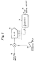
- Fig. 1 shows a block diagram of an A/D converter according to the present invention.
- the numeral 10 shows an A/D converter element, which provides a digital output of the accuracy of 8 bits
- 12 is an adder
- 14 is a calculator
- 16 is an input terminal of an analog signal A in which is subject to convert to digital form
- 18 is a digital output terminal which provides 10 bits of digital signal
- 20 is an input terminal of wobbling signal or dither signal, which is preferably sawtooth wave signal or triangular signal, having the amplitude equal to the minimum resolution value (for instance 10 mV) of the A/D converter element 10.
- the analog input signal at the input terminal 16 and the wobbling input signal 20 are added in the adder 12, and the sum is converted to digital form by the A/D converter element 10 by the accuracy of 8 bits.
- the A/D conversion in the A/D converter element 10 is carried out by a plurality of times (N times) during the slope time of the wobbling signal, and the digital output signals in each A/D conversion operation are accumulated in the calculator 14. After the N-times of A/D conversion operation, the accumulated sum is divided by the number N in the calculator 14, which provides the quotient to the output terminal 18 with the accuracy of 10 bits.
- the preferable value of N is 16 in the embodiment. It should be noted that the calculator 14 provides the average value of 16 outputs of the A/D converter element 10.
- the input value of the A/D converter element 10 is A in + ⁇ V, where the value ⁇ V increases (or decreases) according to the slope of the wobbling signal.
- N-m the digital output for an input analog signal A in
- N-m the digital output for an input analog signal A in
- the value N-m depends upon the relations of A in -(A in ) A/D and the minimum resolution of the A/D converter element. For instance, supposing that the minimum resolution is 10 mV, and A in -(A in ) A/D is 7 mV, the digital output increases by one when ⁇ V>3 mV. Also, if A in -(A in ) A/D is 3 mV, the digital output increases by one when ⁇ V>7 mV.
- N-m that the digital output is (A in ) A/D +1 is proportional to A in -(A in ) A/D .
- the value (N-m)/N is equal to the digital form of A in -(A in ) A/D with the accuracy of log 2 N bits.
- the number of the digital conversion operations (which is 16 in the embodiment) is 2 k , where k is the number of figures of increase. Usually, the number k is in the range of 2 and 4, considering the linearity of the wobbling signal, and undesirable noise.
- the output digital signal would be shifted by some value because of the addition of the wobbling signal in the input side.
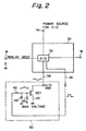
- Fig.2 shows another embodiment of the present invention.
- the features of Fig.2 are that a commercial micro-computer 30 which mounts an A/D converter element 34 is used as an A/D converter element, and that a wobbling signal is added to a reference level of the A/D converter element instead of adding to an input analog signal.
- the reference level of the A/D converter element is ground level
- the ground level of the A/D converter element is modified with the wobbling signal in this case.
- the numeral 32 is a power terminal of the A/D converter element 34
- 38 is a ground terminal of the A/D converter element 34
- 36 is a pulse output signal which shows the actual operation of the A/D conversion element 34.
- the numeral 50 shows a wobbling circuit which provides the sloped wobbling signal based upon said pulse output signal at the terminal 36.
- the wobbling circuit 50 has an FET transistor 40, resistors 42 and 46, and a capacitor 44.
- the resistor 46 is coupled with a bias power supply (not shown).
- the resistor 42 and the capacitor 44 provide an integral circuit which provides the sloped potential according to the rectangular pulse signal at the terminal 36.
- Said rectantular pulse signal is supplied by a micro-computer chip 30 during an A/D converter element 34 operates actually.
- the calculator 14 in Fig.1 is implemented by programming a computer in the embodiment of Fig.2.
- Fig.2 the sloped potential is applied to the terminal 38 so that the reference potential of the A/D converter element 34 is modified according to the sloped wobbling signal. Therefore, it should be appreciated that the embodiment of Fig.2 operates similarly to that of Fig.1.
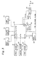
- Fig.3 shows another embodiment of the present invention.
- the feature of Fig.3 is that a micro-computer 30 is coupled with a plurality of sensors 61, 62 and 63, which are for instance a temperature meter and a humidity meter, providing an analog signal.
- the micro-computer 30 carries out the A/D conversion for those analog signals and the digital output signals are displayed on a plurality of liquid crystal display screens 71, 72 and 73 in decimal form.
- the numeral 50 in Fig.3 is the wobbling circuit which is the same as 50 in Fig.2.
- the numeral 80 is a mode selector which instructs the micro-computer 30 the A/D conversion operation
- 82 is a power supply circuit which provides the operational power supply to the micro-computer 30 by using the DC battery supply of 3V.
- the first sensor 61 is for instance a temperature meter.
- the positive value of the temperature is converted to a digital form by a first A/D converter A/D 0
- the negative value of the same is converted by a second A/D converter A/D 1
- the difference (A/D 0 -A/D 1 ) is applied to a first display screen 71.
- the second sensor 62 is for instance a humidity meter, and the analog output of the second sensor is converted to a digital form by the A/D converter A/D 2 and the digital signal is applied to the second display screen 72.
- the third sensor 63 is displayed on the third display screen 73.
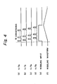
- Fig.4 shows the operational waveforms of Fig.3.
- the waveforms (a), (b), (c) and (d) show the digital output signals of each A/D converter elements each providing 16 digital signals in each operational period
- the waveform (e) is a rectangular pulse signal showing the actual operation of the A/D converter elements
- the waveform (f) is the wobbling signal which is obtained by the integral of the rectangular pulse (e).
- the embodiments describe the case that an 8 bit A/D converter elements provides a digital output signal with the accuracy of 10 bits, the present invention is applicable to the case that a low resolving power A/D converter element provides a higher resolving power digital output signal.
- the present invention is useful in particular to display a digital signal with the accuracy of 0.1 % which is usual in daily life by using a commercial 4 bits micro-computer.
- an adder for adding a wobbling signal to an input analog signal, or a reference potential of an A/D converter is considered.
- An adder has to satisfy the following conditions.
- a conventional adder like a ladder resistor type, or a combination of a ladder resistor and an operational amplifier is not preferable, since the former has resistors for the input of an analog signal and a wobbling signal so that the resistors decrease the input level of both the signals, and the latter has the problem of noise, temperature drift, and/or offset of an operational amplifier which also consumes some power.
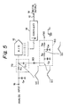
- Fig.5 shows still another embodiment of the present invention, and the feature of Fig.5 resides in an adder 70 which adds a wobbling signal to an input analog signal.
- the same numerals as those in Fig.1 show the same members.
- a capacitor C 01 is coupled between an analog input terminal 16 and ground.
- the input terminal 16 is coupled with an input of the A/D converter element 10 through the resistor R 11 .
- the capacitor C 11 is coupled between the input of the A/D converter element 10 and the integral circuit 60 which has resistors R 21 ,R 22 and capacitors C 21 ,C 22 .
- the input terminal 150 of the integral circuit 60 receives the rectangular waveform (a), which is supplied for instance by a micro-computer chip.
- the resistor R 11 and the capacitor C 11 constitute an integral circuit 70 which integrals an input analog signal at the input terminal 16.
- the capacitor C 01 functions so that the impedance of the analog signal circuit of the input signal does not fluctuate the time constant of the integral circuit 70.
- the input terminal 150 of the integral circuit 60 receives a rectangular pulse signal (a) which is called a dither signal.
- the integral circuit 60 is a double integral circuit.
- the first output (b) of the first integration is a triangular wave as shown in the waveform (b), and the second output of the second integration is shown in the waveform (c).
- the waveform (c) which is the output of the second integration is applied to the input of the A/D converter element 10 through the capacitor C 11 of the integral circuit 70.
- the circuit 70 operates as an integral circuit for the input analog signal at the terminal 16, and simultaneously, operates as a differentiation circuit for the waveform (c) at the terminal 80. Therefore, the wobbling signal (waveform (d)) at the input of the A/D converter element 10 is the same as the waveform (b) which is triangular waveform.
- the rectangular waveform (a) is converted to the triangular waveform (d) through a double integral circuit 60 and a differentiation circuit 70.
- the preferable numeral values for the capacitors and the resistors are as follows.
- a time constant circuit 70 (an integral circuit and/or a differentiation circuit) is usually mounted in a commercial A/D converter. Therefore, the only circuit which one must have in the present invention is an integral circuit 60, which is low in price, and has low power consumption as it uses only passive components.
- the time constant circuit 70 functions as an integral circuit for an input analog signal so that it absorbs noise component. Simultaneously, the time constant circuit 70 functions as a differentiation circuit for a wobbling signal so that the circuit for introducing the wobbling signal has high impedance for an input analog signal, and does not influence to an input analog signal.
- a single integral circuit 60 is provided common to all the analog signals, and the output of the integral circuit 60 is applied to each input terminal 80 of a time constant circuit 70 of each A/D converter element.
- the integral circuit 60 is not a double integral circuit, but a single integral circuit having a single resistor and a single capacitor is used.
Landscapes
- Engineering & Computer Science (AREA)
- Theoretical Computer Science (AREA)
- Analogue/Digital Conversion (AREA)
Claims (7)
- A/D-Umsetzersystem miteinem A/D-Umsetzerelement (10), das ein digitales Ausgangssignal mit einer ersten vorbestimmten Anzahl von Bits erzeugt,einem Linearpotentialmittel zur Erzeugung eines sich linear ändernden Potentials,einem Additionsmittel (12, 70) zum Addieren eines Ausgangssignals des Linearpotentialsmittels zu einem analogen Eingangssignal und zum Eingeben des Ergebnisses in das A/D-Umsetzerelement (10) oder zu einem Bezugspotential des A/D-Umsetzerelements (10),wobei die Maximalamplitude des linearen Potentials im wesentlichen gleich der kleinsten Auflösung des A/D-Umsetzerelements (10) ist,einem Rechner (14) zur Bildung des Mittelwerts mehrerer digitaler Ausgangssignale des A/D-Umsetzerelements mit einer Genauigkeit entsprechend einer zweiten vorbestimmten Anzahl von Bits,wobei die zweite vorbestimmte Anzahl größer als die erste vorbestimmte Anzahl ist,dadurch gekennzeichnet, daß
das Additionsmittel eine Zeitkonstanten-Schaltung ist, die als Integrator für ein analoges Eingangssignal und als Differenzierschaltung für ein schräg verlaufendes Potential wirkt. - A/D-Umsetzersystem nach Anspruch 1, bei dem das Additionsmittel eine Zeitkonstanten-Schaltung (70) mit einem ohmschen Widerstand (R11) und einem Kondensator (C11) am Eingang des A/D-Umsetzerelements ist, so daß ein analoges Eingangssignal dem A/D-Umsetzerelement über den ohmschen Widerstand (R11) und das Potential dem A/D-Umsetzerelement über den Kondensator (C11) zugeführt wird.
- A/D-Umsetzersystem nach Anspruch 1 oder 2, bei dem die erste vorbestimmte Anzahl gleich 8 ist, die zweite vorbestimmte Anzahl gleich 10 ist und der Rechner einen Mittelwert aus 16 digitalen Ausgangssignalen des A/D-Umsetzerelements bildet.
- A/D-Umsetzersystem nach einem der vorstehenden Ansprüche, bei dem das Linearpotentialmittel wenigstens einen Integrator aufweist, dem ein Rechteckimpulssignal zugeführt wird.
- A/D-Umsetzersystem nach Anspruch 4, bei dem das Rechteckimpulssignal ein Tastverhältnis von 50 % hat.
- A/D-Umsetzersystem nach einem der vorstehenden Ansprüche, bei dem das Additionsmittel ein Ausgangssignal des Linearpotentialmittels zu einem analogen Eingangssignal addiert.
- A/D-Umsetzersystem nach Anspruch 1, bei dem das Additionsmittel ein Ausgangssignal des Linearpotentialmittels zu einer Bezugsgröße des A/D-Umsetzerelements addiert.
Applications Claiming Priority (4)
| Application Number | Priority Date | Filing Date | Title |
|---|---|---|---|
| JP18162391A JPH0514201A (ja) | 1991-06-27 | 1991-06-27 | A/d変換装置 |
| JP181623/91 | 1991-06-27 | ||
| JP3275047A JP2626352B2 (ja) | 1991-09-27 | 1991-09-27 | A/d変換装置 |
| JP275047/91 | 1991-09-27 |
Publications (3)
| Publication Number | Publication Date |
|---|---|
| EP0520662A2 EP0520662A2 (de) | 1992-12-30 |
| EP0520662A3 EP0520662A3 (en) | 1993-09-22 |
| EP0520662B1 true EP0520662B1 (de) | 1997-04-23 |
Family
ID=26500732
Family Applications (1)
| Application Number | Title | Priority Date | Filing Date |
|---|---|---|---|
| EP92305475A Expired - Lifetime EP0520662B1 (de) | 1991-06-27 | 1992-06-15 | Analog-Digitalumsetzer mit erhöhter Auflösung |
Country Status (3)
| Country | Link |
|---|---|
| US (1) | US5305005A (de) |
| EP (1) | EP0520662B1 (de) |
| DE (1) | DE69219216T2 (de) |
Families Citing this family (10)
| Publication number | Priority date | Publication date | Assignee | Title |
|---|---|---|---|---|
| US5416481A (en) * | 1993-09-24 | 1995-05-16 | Advanced Micro Devices, Inc. | Analog-to-digital converter with multi-level dither current input |
| FR2738978B1 (fr) * | 1995-09-15 | 1997-10-17 | Thomson Multimedia Sa | Procede pour la numerisation de signaux a frequence intermediaire fi en particulier de signaux video et circuit pour la mise en oeuvre de ce procede |
| US6016113A (en) * | 1997-06-26 | 2000-01-18 | Binder; Yehuda | System for enhancing the accuracy of analog-digital-analog conversions |
| DE102004020264A1 (de) * | 2004-04-26 | 2005-11-17 | Infineon Technologies Ag | Analog-Digital-Wandler und Verfahren zum Wandeln eines analogen Messsignals |
| US7161392B2 (en) * | 2004-06-23 | 2007-01-09 | Teradyne, Inc. | Comparator feedback peak detector |
| DE102005001733A1 (de) | 2005-01-14 | 2006-07-27 | Robert Bosch Gmbh | Analog-Digital-Umsetzer |
| US20070252747A1 (en) * | 2006-04-28 | 2007-11-01 | Colin Lyden | No-missing-code analog to digital converter system and method |
| IL231163A (en) | 2014-02-26 | 2016-05-31 | Elta Systems Ltd | A system and method for improving the dynamic range of a multi-channel digital receiver that targets transmitted signals |
| DE102014219531A1 (de) * | 2014-09-26 | 2016-03-31 | Continental Teves Ag & Co. Ohg | Vorrichtung zum Digitalisieren eines analogen Signals |
| DE102016204417A1 (de) * | 2016-03-17 | 2017-09-21 | Continental Teves Ag & Co. Ohg | Vorrichtung zum Messen einer Messgröße |
Family Cites Families (11)
| Publication number | Priority date | Publication date | Assignee | Title |
|---|---|---|---|---|
| FR2232881A1 (en) * | 1973-06-08 | 1975-01-03 | Anvar | Parallel analogue-digital converter - for digital measurement of analogue electrical signals using series of comparators |
| US4144577A (en) * | 1977-10-14 | 1979-03-13 | The United States Of America As Represented By The Secretary Of The Air Force | Integrated quantized signal smoothing processor |
| US4417234A (en) * | 1981-12-03 | 1983-11-22 | The Singer Company | Multiplexed analog to digital converter having a feedback stabilized ramp |
| DE3212103A1 (de) * | 1982-04-01 | 1983-10-06 | Licentia Gmbh | Verfahren und anordnung zur analog/digital-umsetzung |
| GB2144285B (en) * | 1983-07-29 | 1986-09-24 | Raymond Allan Belcher | Analague-to-digital and digital-to-analogue conversion |
| EP0167412B1 (de) * | 1984-07-06 | 1991-06-05 | British Aerospace | Analog-Digital-Umwandlung |
| JPH0611114B2 (ja) * | 1984-12-31 | 1994-02-09 | ティアツク株式会社 | アナログ−ディジタル変換装置 |
| JPH0738588B2 (ja) * | 1985-07-11 | 1995-04-26 | ティアツク株式会社 | アナログ―デイジタル変換装置 |
| JPH07118649B2 (ja) * | 1986-01-08 | 1995-12-18 | ヤマハ株式会社 | デイザ回路 |
| JPH02134010A (ja) * | 1988-11-15 | 1990-05-23 | Sony Corp | 信号処理装置 |
| EP0444234B1 (de) * | 1990-03-02 | 1995-06-07 | Siemens-Elema AB | Verfahren und Einrichtung zur Analog-Digital-Wandlung |
-
1992
- 1992-06-11 US US07/897,152 patent/US5305005A/en not_active Expired - Fee Related
- 1992-06-15 EP EP92305475A patent/EP0520662B1/de not_active Expired - Lifetime
- 1992-06-15 DE DE69219216T patent/DE69219216T2/de not_active Expired - Fee Related
Also Published As
| Publication number | Publication date |
|---|---|
| US5305005A (en) | 1994-04-19 |
| EP0520662A2 (de) | 1992-12-30 |
| EP0520662A3 (en) | 1993-09-22 |
| DE69219216D1 (de) | 1997-05-28 |
| DE69219216T2 (de) | 1997-08-07 |
Similar Documents
| Publication | Publication Date | Title |
|---|---|---|
| US4357600A (en) | Multislope converter and conversion technique | |
| US5305005A (en) | Analog to digital converter system | |
| US5519397A (en) | Circuit for processing the output signal from a resistive analog sensor, in particular for the fuel gauge of a motor vehicle, and systems fitted therewith | |
| US4647905A (en) | Improved pulse-width-modulation signal converter | |
| US3868677A (en) | Phase-locked voltage-to-digital converter | |
| US4567466A (en) | Sensor communication system | |
| CN1140260A (zh) | 用于测量双联电容器电容值变化的方法和装置 | |
| EP0434248A2 (de) | Anordnungen zur elektrischen Leistungsmessung | |
| US4912660A (en) | Method and apparatus for measurements of a characteristic of an object using a sensed signal and an auxiliary variable signal applied to the object | |
| US4034367A (en) | Analog-to-digital converter utilizing a random noise source | |
| US4214479A (en) | Capacitive type fuel probe compensation circuit | |
| US4486706A (en) | Power flow direction detector | |
| EP0670499A1 (de) | Spannungs-Frequenzwandler | |
| EP0749084A2 (de) | Direkt-digital-Synthesierer | |
| US4672236A (en) | Voltage-to-frequency converter circuit | |
| US3934198A (en) | Multi-wire electronic kWh meter | |
| JP2626352B2 (ja) | A/d変換装置 | |
| JPH0514201A (ja) | A/d変換装置 | |
| US4967099A (en) | Low level clamp circuit | |
| JP4422284B2 (ja) | A/d変換器及び半導体圧力センサ装置 | |
| AU760698B2 (en) | Frequency to frequency de-randomiser circuit | |
| GB1597288A (en) | Power monitoring devices | |
| Stockton | A simple, highly linear mark: space ratio digital-to-analogue converter | |
| JP3453826B2 (ja) | 積分値または平均値を得る演算器 | |
| GB2120481A (en) | Improvements in or relating to analogue to digital converters |
Legal Events
| Date | Code | Title | Description |
|---|---|---|---|
| PUAI | Public reference made under article 153(3) epc to a published international application that has entered the european phase |
Free format text: ORIGINAL CODE: 0009012 |
|
| 17P | Request for examination filed |
Effective date: 19920703 |
|
| AK | Designated contracting states |
Kind code of ref document: A2 Designated state(s): DE FR GB NL |
|
| PUAL | Search report despatched |
Free format text: ORIGINAL CODE: 0009013 |
|
| AK | Designated contracting states |
Kind code of ref document: A3 Designated state(s): DE FR GB NL |
|
| 17Q | First examination report despatched |
Effective date: 19960207 |
|
| GRAG | Despatch of communication of intention to grant |
Free format text: ORIGINAL CODE: EPIDOS AGRA |
|
| GRAH | Despatch of communication of intention to grant a patent |
Free format text: ORIGINAL CODE: EPIDOS IGRA |
|
| GRAH | Despatch of communication of intention to grant a patent |
Free format text: ORIGINAL CODE: EPIDOS IGRA |
|
| GRAA | (expected) grant |
Free format text: ORIGINAL CODE: 0009210 |
|
| AK | Designated contracting states |
Kind code of ref document: B1 Designated state(s): DE FR GB NL |
|
| REF | Corresponds to: |
Ref document number: 69219216 Country of ref document: DE Date of ref document: 19970528 |
|
| ET | Fr: translation filed | ||
| PLBE | No opposition filed within time limit |
Free format text: ORIGINAL CODE: 0009261 |
|
| STAA | Information on the status of an ep patent application or granted ep patent |
Free format text: STATUS: NO OPPOSITION FILED WITHIN TIME LIMIT |
|
| 26N | No opposition filed | ||
| REG | Reference to a national code |
Ref country code: GB Ref legal event code: IF02 |
|
| PGFP | Annual fee paid to national office [announced via postgrant information from national office to epo] |
Ref country code: FR Payment date: 20020610 Year of fee payment: 11 |
|
| PGFP | Annual fee paid to national office [announced via postgrant information from national office to epo] |
Ref country code: GB Payment date: 20020612 Year of fee payment: 11 |
|
| PGFP | Annual fee paid to national office [announced via postgrant information from national office to epo] |
Ref country code: DE Payment date: 20020619 Year of fee payment: 11 |
|
| PGFP | Annual fee paid to national office [announced via postgrant information from national office to epo] |
Ref country code: NL Payment date: 20020628 Year of fee payment: 11 |
|
| PG25 | Lapsed in a contracting state [announced via postgrant information from national office to epo] |
Ref country code: GB Free format text: LAPSE BECAUSE OF NON-PAYMENT OF DUE FEES Effective date: 20030615 |
|
| PG25 | Lapsed in a contracting state [announced via postgrant information from national office to epo] |
Ref country code: NL Free format text: LAPSE BECAUSE OF NON-PAYMENT OF DUE FEES Effective date: 20040101 Ref country code: DE Free format text: LAPSE BECAUSE OF NON-PAYMENT OF DUE FEES Effective date: 20040101 |
|
| GBPC | Gb: european patent ceased through non-payment of renewal fee |
Effective date: 20030615 |
|
| PG25 | Lapsed in a contracting state [announced via postgrant information from national office to epo] |
Ref country code: FR Free format text: LAPSE BECAUSE OF NON-PAYMENT OF DUE FEES Effective date: 20040227 |
|
| NLV4 | Nl: lapsed or anulled due to non-payment of the annual fee |
Effective date: 20040101 |
|
| REG | Reference to a national code |
Ref country code: FR Ref legal event code: ST |